Digital Circuit Design for Minimum Transient Energy Vishwani
- Slides: 24

Digital Circuit Design for Minimum Transient Energy Vishwani D. Agrawal Circuits and Systems Research Lab, Agere Systems (Bell Labs, Lucent Tech. ) Murray Hill, NJ 07974 va@research. bell-labs. com http: //cm. bell-labs. com/cm/cs/who/va Research Collaborators: Nov. 8, 00 M. L. Bushnell, Rutgers University R. Ramadoss, Lucent Microelectronics G. Parthasarathy, UC Santa Barbara Low-Power Design 1

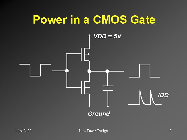
Power in a CMOS Gate VDD = 5 V IDD Ground Nov. 8, 00 Low-Power Design 2

Motivation • Low power applications • Remote systems (e. g. , satellite) • Portable systems (e. g. , mobile phone) • Methods of low power design • Reduced supply voltage • Adiabatic switching • Clock suppression • Logic design for reduced activity • Reduce Hazards (40% in arithmetic logic) • Software techniques • Reference: Chandrakasan and Brodersen Nov. 8, 00 Low-Power Design 3

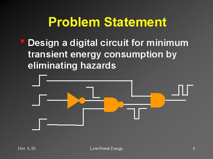
Problem Statement • Design a digital circuit for minimum transient energy consumption by eliminating hazards Nov. 8, 00 Low-Power Design 4

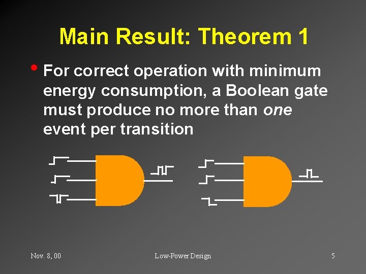
Main Result: Theorem 1 • For correct operation with minimum energy consumption, a Boolean gate must produce no more than one event per transition Nov. 8, 00 Low-Power Design 5

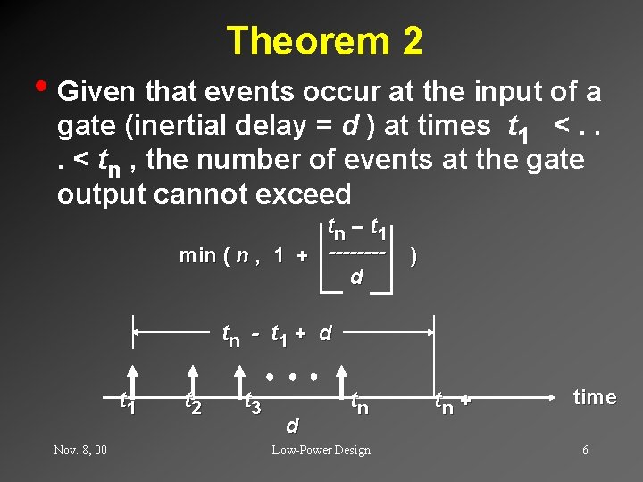
Theorem 2 • Given that events occur at the input of a gate (inertial delay = d ) at times t 1 <. . . < tn , the number of events at the gate output cannot exceed tn – t 1 min ( n , 1 + -------d ) tn - t 1 + d t 1 Nov. 8, 00 t 2 t 3 d tn Low-Power Design tn + time 6

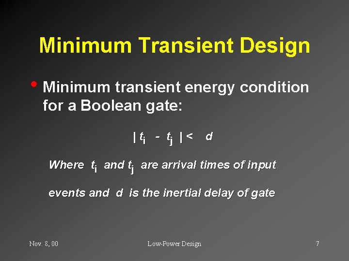
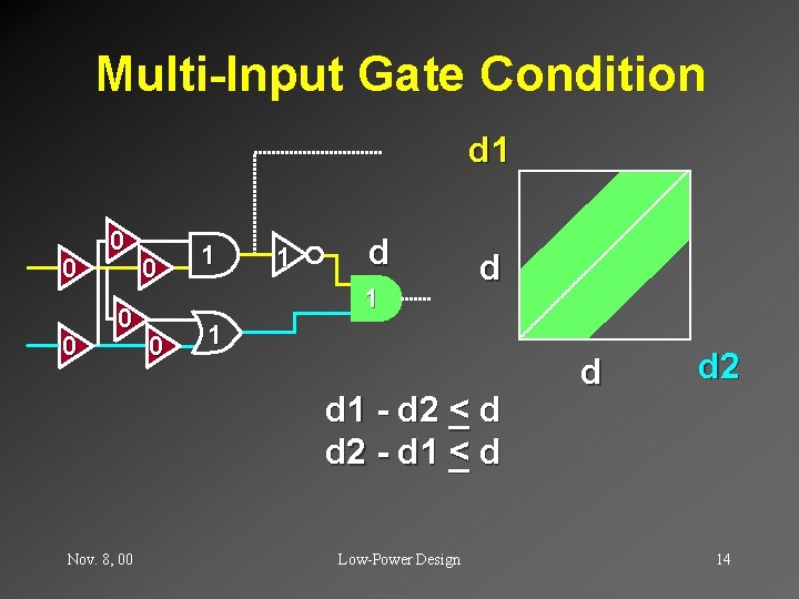
Minimum Transient Design • Minimum transient energy condition for a Boolean gate: | ti - tj | < d Where ti and tj are arrival times of input events and d is the inertial delay of gate Nov. 8, 00 Low-Power Design 7

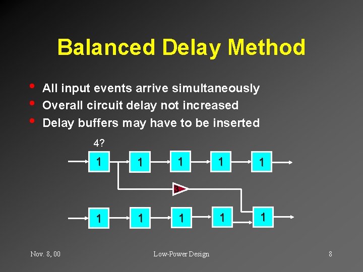
Balanced Delay Method • • • All input events arrive simultaneously Overall circuit delay not increased Delay buffers may have to be inserted 4? 1 1 1 1 3 1 Nov. 8, 00 1 1 Low-Power Design 8

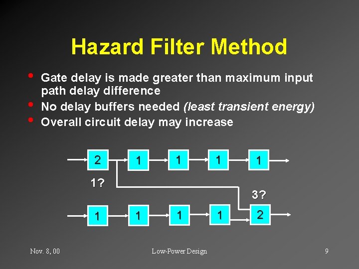
Hazard Filter Method • • • Gate delay is made greater than maximum input path delay difference No delay buffers needed (least transient energy) Overall circuit delay may increase 2 1 1? 1 Nov. 8, 00 1 3? 1 1 Low-Power Design 1 2 9

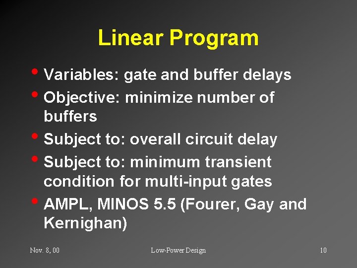
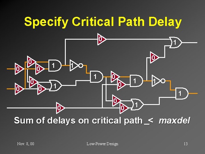
Linear Program • Variables: gate and buffer delays • Objective: minimize number of • • • buffers Subject to: overall circuit delay Subject to: minimum transient condition for multi-input gates AMPL, MINOS 5. 5 (Fourer, Gay and Kernighan) Nov. 8, 00 Low-Power Design 10

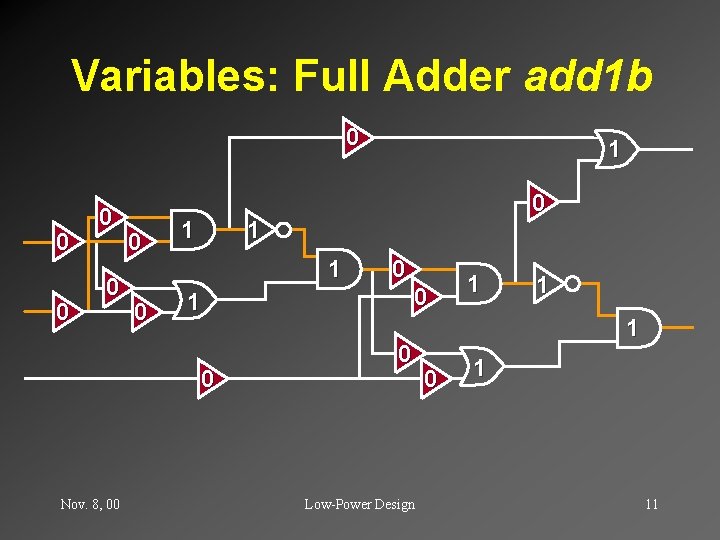
Variables: Full Adder add 1 b 0 0 0 0 1 1 1 0 Nov. 8, 00 1 0 0 Low-Power Design 1 1 1 0 1 11

Objective Function • Ideal: minimize the number of non • zero delay buffers Actual: sum of buffer delays Nov. 8, 00 Low-Power Design 12

Specify Critical Path Delay 0 0 0 0 1 1 1 0 1 Sum of delays on critical path _< maxdel Nov. 8, 00 Low-Power Design 13

Multi-Input Gate Condition d 1 0 0 0 1 1 d d 1 - d 2 < _d d 2 - d 1 < _d Nov. 8, 00 Low-Power Design d d 2 14

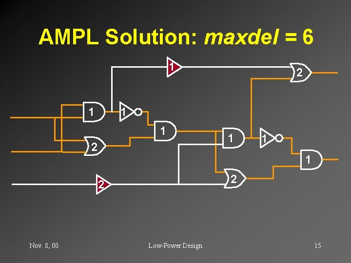
AMPL Solution: maxdel = 6 1 1 2 1 1 1 2 2 Nov. 8, 00 2 Low-Power Design 15

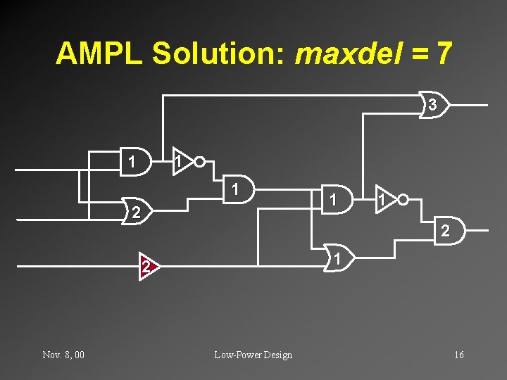
AMPL Solution: maxdel = 7 3 1 1 1 2 1 2 Nov. 8, 00 1 Low-Power Design 16

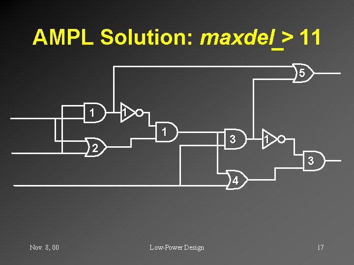
AMPL Solution: maxdel_> 11 5 1 1 1 2 3 1 3 4 Nov. 8, 00 Low-Power Design 17

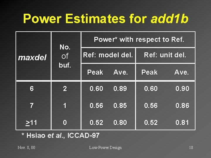
Power Estimates for add 1 b No. maxdel of buf. Power* with respect to Ref: model del. Ref: unit del. Peak Ave. 6 2 0. 60 0. 89 0. 60 0. 90 7 1 0. 56 0. 85 0. 56 0. 86 _ >11 0 0. 52 0. 81 * Hsiao et al. , ICCAD-97 Nov. 8, 00 Low-Power Design 18

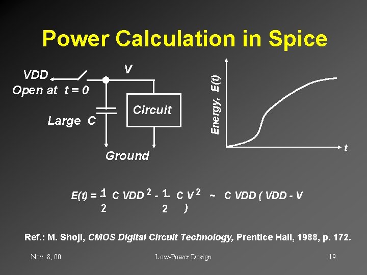
VDD Open at t = 0 Large C V Circuit Energy, E(t) Power Calculation in Spice t Ground E(t) = --1 C VDD 2 - 1 -- C V 2 ~ C VDD ( VDD - V ) 2 2 Ref. : M. Shoji, CMOS Digital Circuit Technology, Prentice Hall, 1988, p. 172. Nov. 8, 00 Low-Power Design 19

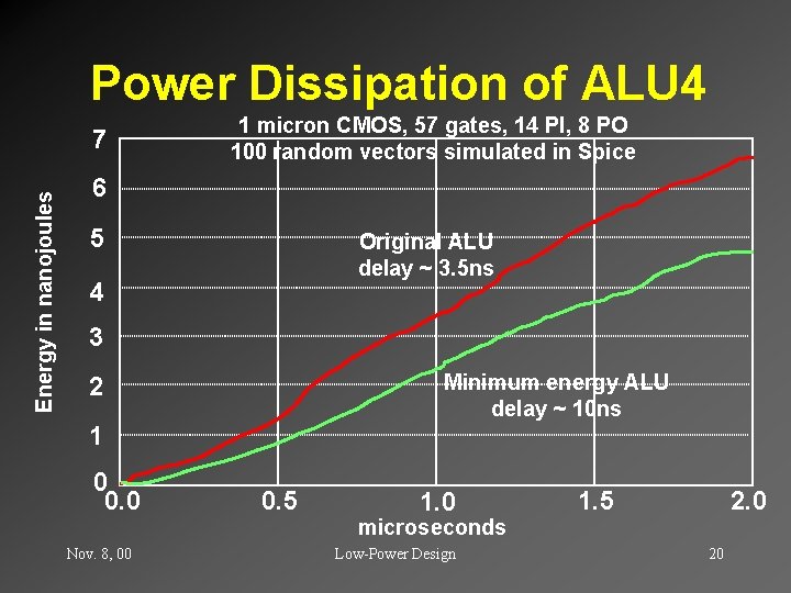
Power Dissipation of ALU 4 Energy in nanojoules 7 1 micron CMOS, 57 gates, 14 PI, 8 PO 100 random vectors simulated in Spice 6 5 Original ALU delay ~ 3. 5 ns 4 3 Minimum energy ALU delay ~ 10 ns 2 1 0 0. 5 1. 0 1. 5 2. 0 microseconds Nov. 8, 00 Low-Power Design 20

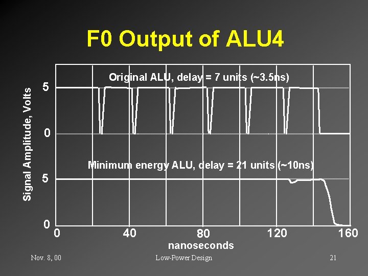
Signal Amplitude, Volts F 0 Output of ALU 4 Original ALU, delay = 7 units (~3. 5 ns) 5 0 Minimum energy ALU, delay = 21 units (~10 ns) 5 0 0 40 80 120 160 nanoseconds Nov. 8, 00 Low-Power Design 21

Some Comments • J. Bentley: Path enumeration may be • • avoided by retiming type algorithms; Leiserson and Saxe, Ph. D theses M. Yannakakis: Use ellipsoid method if you can verify a solution in linear time; also try partitioning approach M. Wright: Use ILP Nov. 8, 00 Low-Power Design 22

References • • E. Jacobs and M. Berkelaar, “Using Gate Sizing to Reduce Glitch Power, ” Proc. Pro. RISC/IEEE Workshop on Circuits, Systems and Signal Processing, Nov. 1996, pp. 183 -188; also Int. Workshop on Logic Synthesis, May 1997. V. D. Agrawal, “Low-Power Design by Hazard Filtering, ” Proc. 10 th Int. Conf. VLSI Design, Jan. 1997, pp. 193 -197. V. D. Agrawal, M. L. Bushnell, G. Parthasarathy, and R. Ramadoss, “Digital Circuit Design for Minimum Transient Energy and a Linear Programming Method, ” Proc. 12 th Int. Conf. VLSI Design, Jan. 1999, pp. 434 -439. Last two papers are available at website http: //cm. belllabs. com/cm/cs/who/va Nov. 8, 00 Low-Power Design 23

Conclusion • • Linear programming gives optimum design Analysis may reduce the number of constraints Technique can be applied to partitioned circuit An alternative min-flow formulation avoids path enumeration (approximate method) Transistor-sizing problem can be reformulated for area, delay and power reduction Glitch-free circuits have better timing properties Applications to CPU time reduction in programs and in project management for reduced cost Nov. 8, 00 Low-Power Design 24