AIDEMC Low Emission Digital Circuit Design Department of
- Slides: 25

AID–EMC: Low Emission Digital Circuit Design Department of Electrical Engineering (ESAT) MICAS Design-In for EMC on digital circuit October 27 th, 2005 Junfeng Zhou Wim Dehaene KULeuven ESAT-MICAS

Outline Department of Electrical Engineering (ESAT) 1. 2. 2. 3. 3. 4. MICAS Introduction Logic family selection Clock strategy selection (not discuss today due to lack of time) 1. clock skew 2. SSCG 3. Delay cell array approach Low noise power supply – EMI reducer 1. continuous time 2. stability analysis 3. future work

Part I: Introduction Department of Electrical Engineering (ESAT) MICAS Electro-Magnetic Interference (EMI) and radiated emission have become a major problem for high speed digital circuit, Most of them are due to power and ground fluctuation. Although the detailed calculation of EMI noise is rather difficult , we can use the di/dt as the index, since the current loop contributes the EMI.

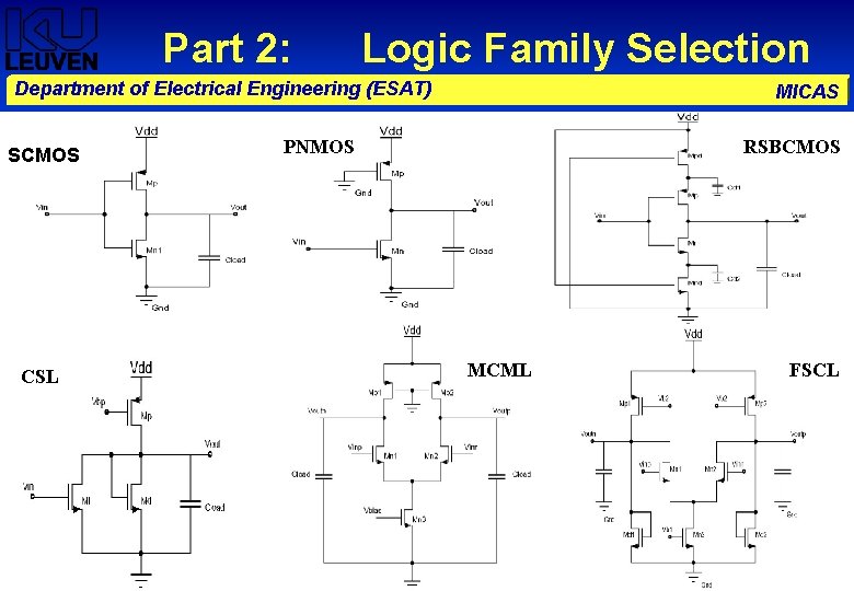
Part 2: Logic Family Selection Department of Electrical Engineering (ESAT) SCMOS CSL MICAS PNMOS RSBCMOS MCML FSCL

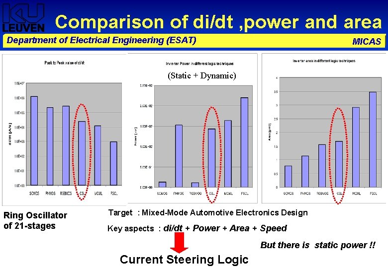
Comparison of di/dt , power and area Department of Electrical Engineering (ESAT) MICAS (Static + Dynamic) Ring Oscillator of 21 -stages Target : Mixed-Mode Automotive Electronics Design Key aspects : di/dt + Power + Area + Speed But there is static power !! Current Steering Logic

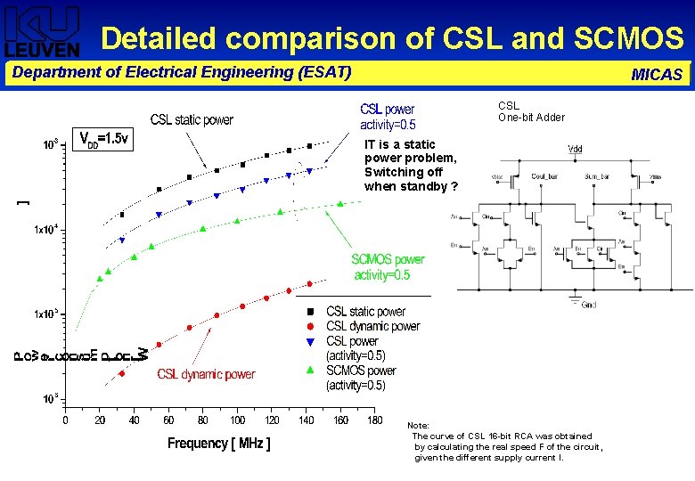
Detailed comparison of CSL and SCMOS Department of Electrical Engineering (ESAT) MICAS CSL One-bit Adder IT is a static power problem, Switching off when standby ? Note: The curve of CSL 16 -bit RCA was obtained by calculating the real speed F of the circuit, given the different supply current I.

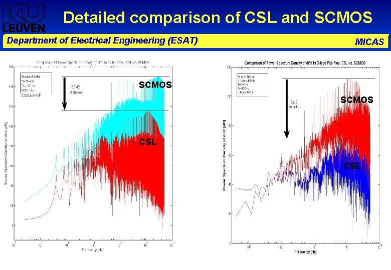
Detailed comparison of CSL and SCMOS Department of Electrical Engineering (ESAT) MICAS SCMOS CSL

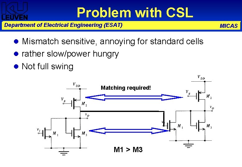
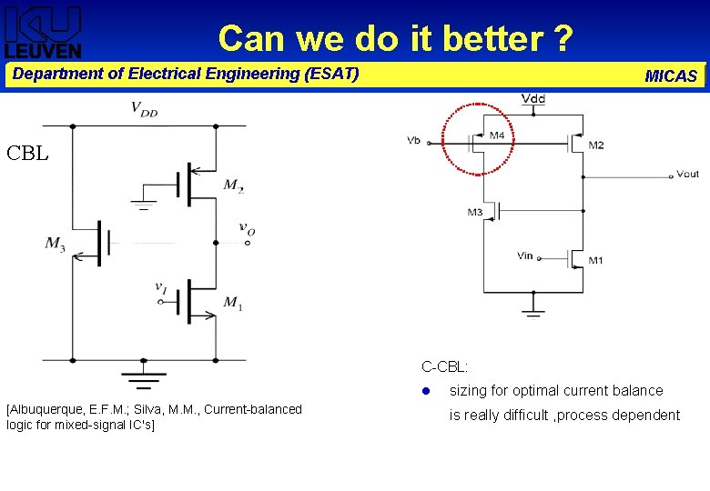
Problem with CSL Department of Electrical Engineering (ESAT) Mismatch sensitive, annoying for standard cells rather slow/power hungry Not full swing Matching required! M 1 > M 3 MICAS

Can we do it better ? Department of Electrical Engineering (ESAT) MICAS CBL C-CBL: [Albuquerque, E. F. M. ; Silva, M. M. , Current-balanced logic for mixed-signal IC's] sizing for optimal current balance is really difficult , process dependent

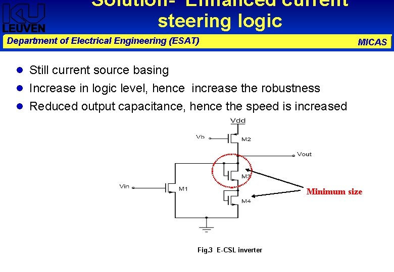
Solution- Enhanced current steering logic Department of Electrical Engineering (ESAT) MICAS Still current source basing Increase in logic level, hence increase the robustness Reduced output capacitance, hence the speed is increased Minimum size Fig. 3 E-CSL inverter

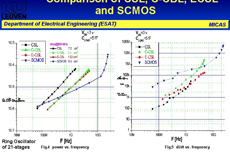
Comparison of CSL, C-CBL, ECSL and SCMOS Department of Electrical Engineering (ESAT) Ring Oscillator of 21 -stages Fig. 4 power vs. frequency MICAS Fig. 5 di/dt vs. frequency

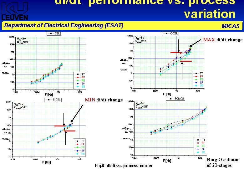
di/dt performance vs. process variation Department of Electrical Engineering (ESAT) MICAS MAX di/dt change MIN di/dt change Fig. 6 di/dt vs. process corner Ring Oscillator of 21 -stages

Conclusion of Low noise Logic Families Department of Electrical Engineering (ESAT) CSL, E-CSL show a smaller area per logic function for MICAS complex digital gates and systems compared to SCMOS logic technique. Current source ensures the major di/dt reduction, Process variation sensitivity also becomes better due to the dominance of current source, E-CSL gives comparable di/dt performance with CSL, E-CSL is Faster and Less power consuming than CSL due to the lower area and lower capacitance. Static power consumption remains the challenge for wide application of the CSL, E-CSL technique in very large digital systems. Can be solved by using power down strategies, which is highly application dependent Winner is E-CSL

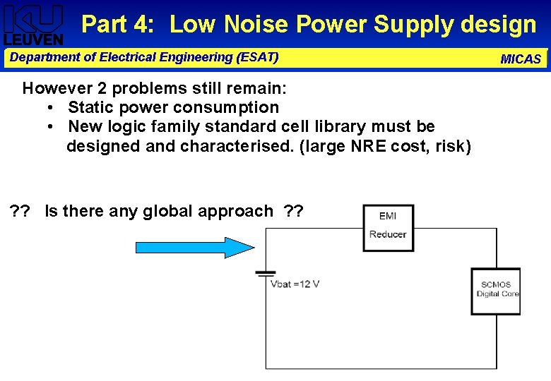
Part 4: Low Noise Power Supply design Department of Electrical Engineering (ESAT) However 2 problems still remain: • Static power consumption • New logic family standard cell library must be designed and characterised. (large NRE cost, risk) ? ? Is there any global approach ? ? MICAS

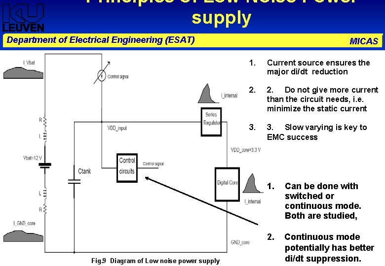
Principles of Low Noise Power supply Department of Electrical Engineering (ESAT) Fig. 9 Diagram of Low noise power supply MICAS 1. Current source ensures the major di/dt reduction 2. Do not give more current than the circuit needs, i. e. minimize the static current 3. Slow varying is key to EMC success 1. Can be done with switched or continuous mode. Both are studied, 2. Continuous mode potentially has better di/dt suppression.

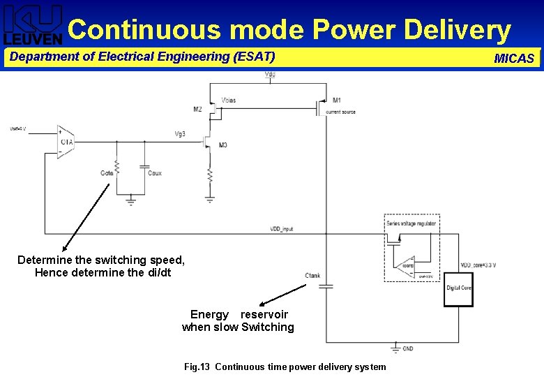
Continuous mode Power Delivery Department of Electrical Engineering (ESAT) Determine the switching speed, Hence determine the di/dt Energy reservoir when slow Switching Fig. 13 Continuous time power delivery system MICAS

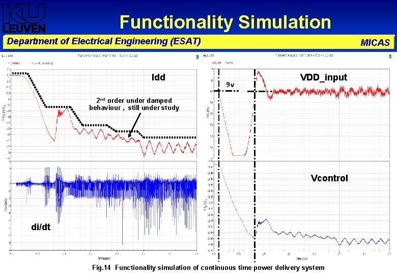
Functionality Simulation Department of Electrical Engineering (ESAT) Idd MICAS 9 v VDD_input 2 nd order under damped behaviour , still under study continuous time OTA feedback loop stable Vcontrol di/dt Fig. 14 Functionality simulation of continuous time power delivery system

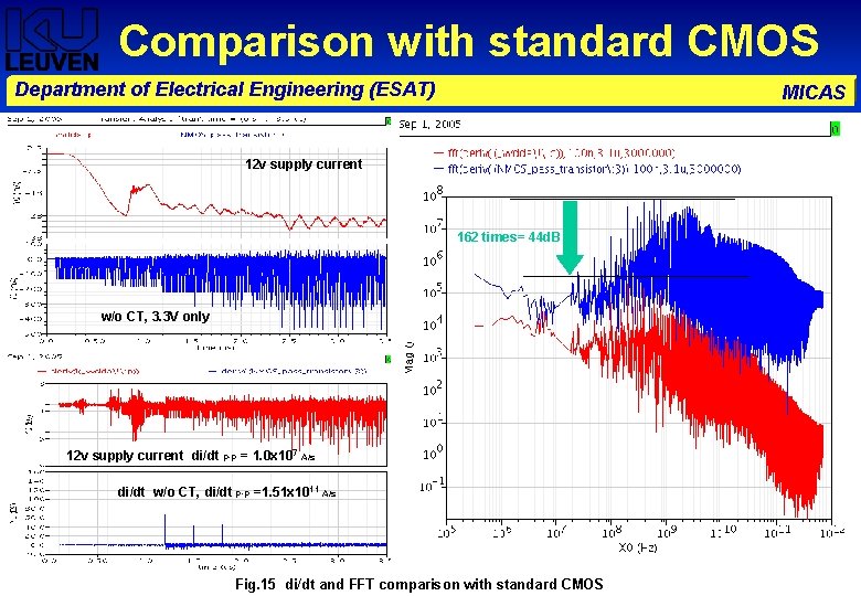
Comparison with standard CMOS Department of Electrical Engineering (ESAT) MICAS 12 v supply current 162 times= 44 d. B w/o CT, 3. 3 V only 12 v supply current di/dt p-p = 1. 0 x 107 A/s di/dt w/o CT, di/dt p-p =1. 51 x 1011 A/s Fig. 15 di/dt and FFT comparison with standard CMOS

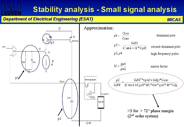
Stability analysis - Small signal analysis Department of Electrical Engineering (ESAT) MICAS Approximation: dominant pole p 3 second-dominant pole high frequency poles p 4 mirror factor p 1 p 2 >3 for > 72° phase margin (2 nd order system)

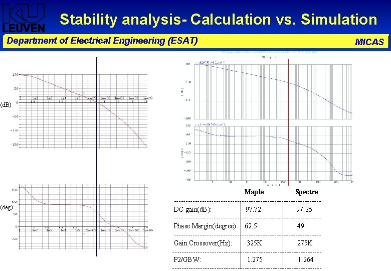
Stability analysis- Calculation vs. Simulation Department of Electrical Engineering (ESAT) (d. B) (deg) Maple Spectre -------------------------------DC gain(d. B): 97. 72 97. 25 -------------------------------Phase Margin(degree): 62. 5 49 -------------------------------Gain Crossover(Hz): 325 K 275 K --------------------------------P 2/GBW: 1. 275 1. 264 -------------------------------- MICAS

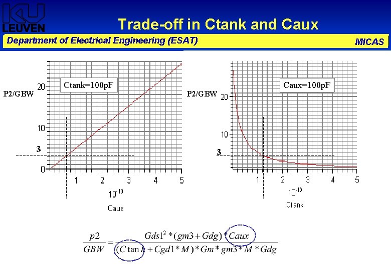
Trade-off in Ctank and Caux Department of Electrical Engineering (ESAT) Ctank=100 p. F P 2/GBW 3 MICAS P 2/GBW 3 Caux=100 p. F

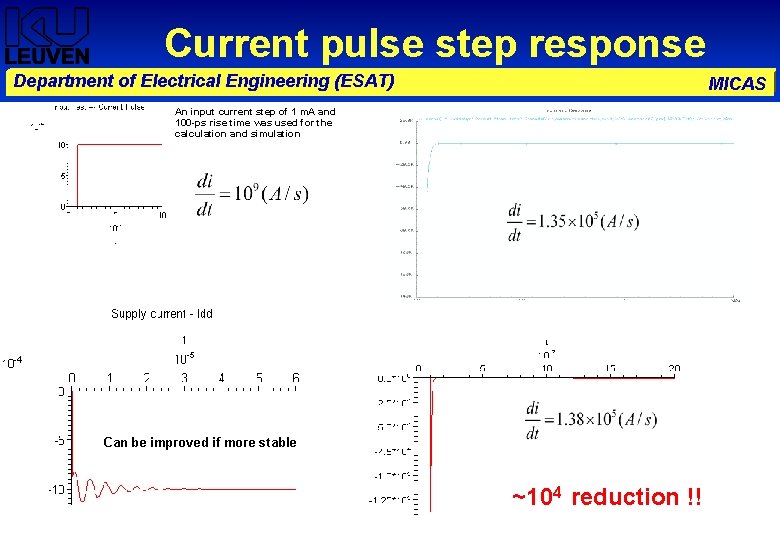
Current pulse step response Department of Electrical Engineering (ESAT) MICAS An input current step of 1 m. A and 100 -ps rise time was used for the calculation and simulation Can be improved if more stable ~104 reduction !!

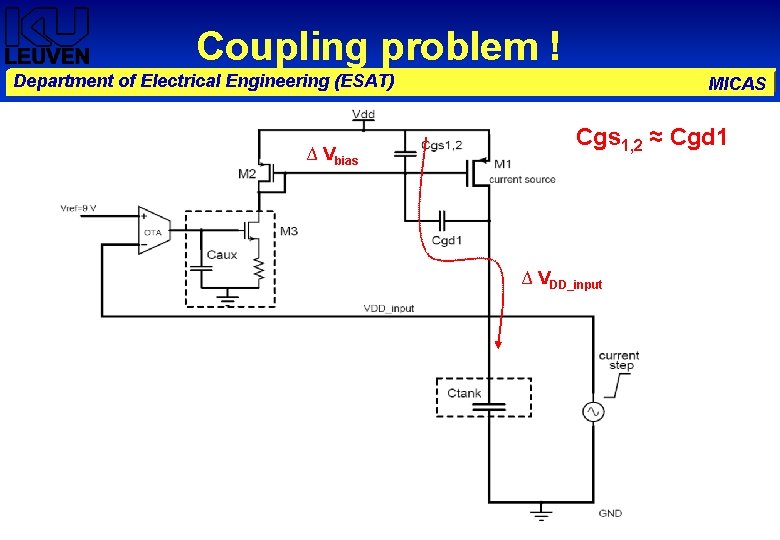
Coupling problem ! Department of Electrical Engineering (ESAT) ∆ Vbias MICAS Cgs 1, 2 ≈ Cgd 1 ∆ VDD_input

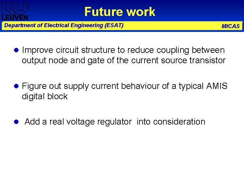
Future work Department of Electrical Engineering (ESAT) MICAS Improve circuit structure to reduce coupling between output node and gate of the current source transistor Figure out supply current behaviour of a typical AMIS digital block Add a real voltage regulator into consideration

Questions Department of Electrical Engineering (ESAT) Thank you for your attention MICAS