AIDEMC Low Emission Digital Circuit Design Department of
- Slides: 21

AID–EMC: Low Emission Digital Circuit Design Department of Electrical Engineering (ESAT) MICAS Status of the “Digital EMC project” Junfeng Zhou Wim Dehaene

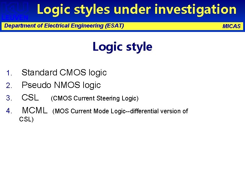
Logic styles under investigation Department of Electrical Engineering (ESAT) Logic style 1. 2. 3. 4. Standard CMOS logic Pseudo NMOS logic CSL (CMOS Current Steering Logic) MCML (MOS Current Mode Logic--differential version of CSL) MICAS

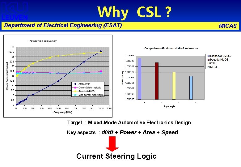
Why CSL ? Department of Electrical Engineering (ESAT) Target : Mixed-Mode Automotive Electronics Design Key aspects : di/dt + Power + Area + Speed Current Steering Logic MICAS

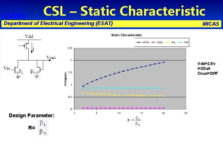
CSL – Static Characteristic Department of Electrical Engineering (ESAT) MICAS Vdd=2. 5 v I=20 u. A Cload=20 f. F Design Parameter: R=

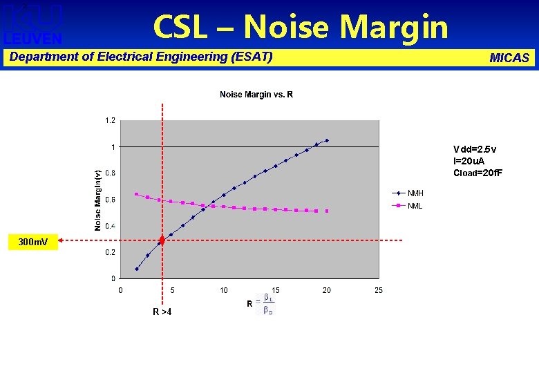
CSL – Noise Margin Department of Electrical Engineering (ESAT) MICAS Vdd=2. 5 v I=20 u. A Cload=20 f. F 300 m. V R >4

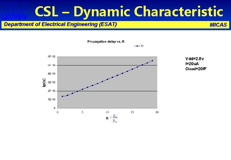
CSL – Dynamic Characteristic Department of Electrical Engineering (ESAT) MICAS Vdd=2. 5 v I=20 u. A Cload=20 f. F

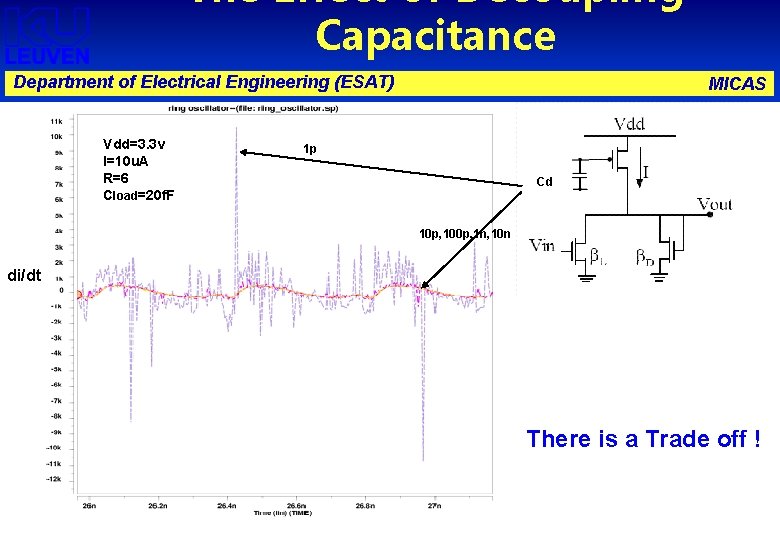
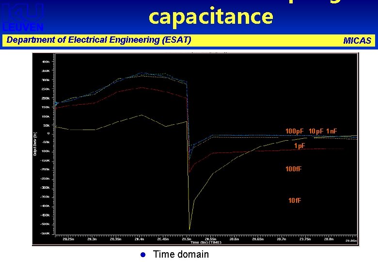
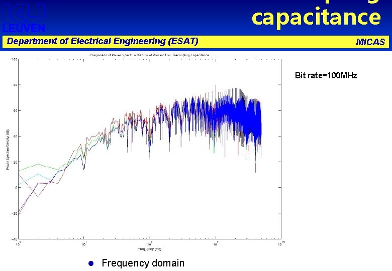
The Effect of Decoupling Capacitance Department of Electrical Engineering (ESAT) Vdd=3. 3 v I=10 u. A R=6 Cload=20 f. F MICAS 1 p Cd 10 p, 100 p, 1 n, 10 n di/dt There is a Trade off !

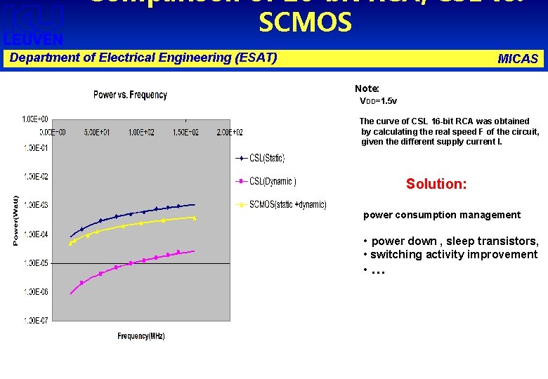
Comparison of 16 -bit RCA, CSL vs. SCMOS Department of Electrical Engineering (ESAT) MICAS Note: VDD=1. 5 v The curve of CSL 16 -bit RCA was obtained by calculating the real speed F of the circuit, given the different supply current I. Solution: power consumption management • power down , sleep transistors, • switching activity improvement • …

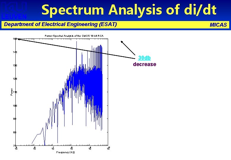
Spectrum Analysis of di/dt Department of Electrical Engineering (ESAT) MICAS Power Spectral Analysis of the CMOS 16 -bit RCA 150 140 30 db decrease 130 Power 120 110 100 90 80 705 10 6 10 7 10 8 10 Frequency (Hz) 9 10 10 10

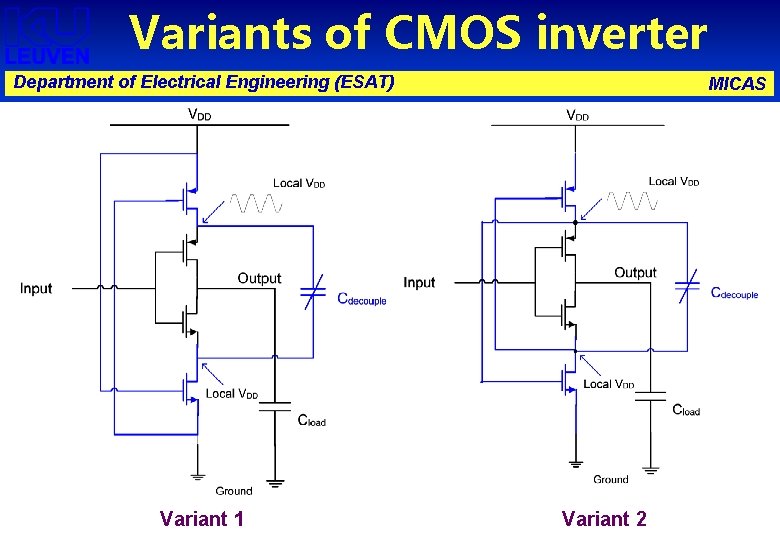
Variants of CMOS inverter Department of Electrical Engineering (ESAT) Variant 1 MICAS Variant 2

capacitance Department of Electrical Engineering (ESAT) MICAS 100 p. F 1 n. F 1 p. F 100 f. F 10 f. F l Time domain

capacitance Department of Electrical Engineering (ESAT) MICAS Bit rate=100 MHz l Frequency domain

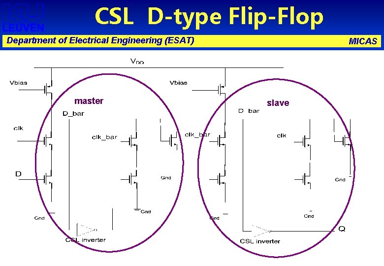
CSL D-type Flip-Flop Department of Electrical Engineering (ESAT) master MICAS slave

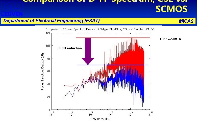
Comparison of D-FF Spectrum, CSL vs. SCMOS Department of Electrical Engineering (ESAT) MICAS Clock=50 MHz 38 d. B reduction

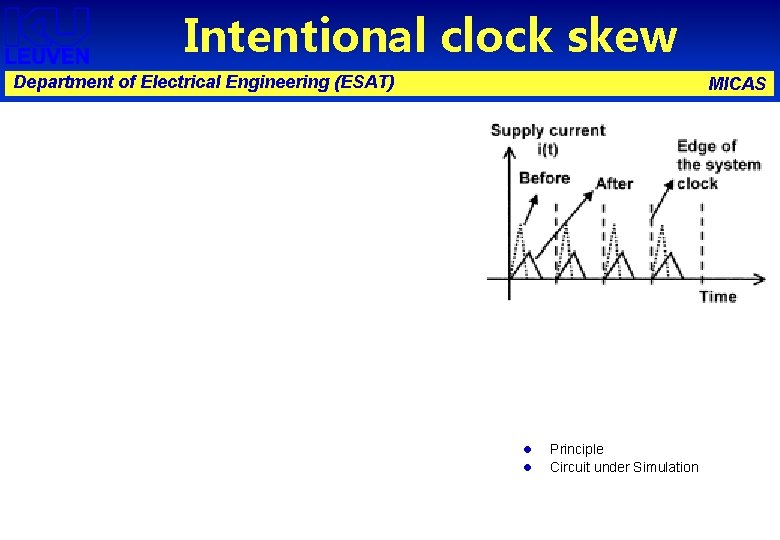
Intentional clock skew Department of Electrical Engineering (ESAT) MICAS l l Principle Circuit under Simulation

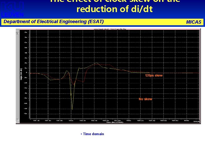
The effect of clock skew on the reduction of di/dt Department of Electrical Engineering (ESAT) MICAS 120 ps skew No skew • Time domain

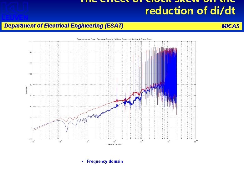
The effect of clock skew on the reduction of di/dt Department of Electrical Engineering (ESAT) • Frequency domain MICAS

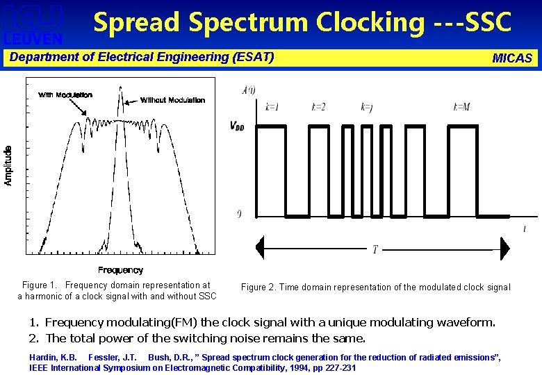
Spread Spectrum Clocking ---SSC Department of Electrical Engineering (ESAT) Figure 1. Frequency domain representation at a harmonic of a clock signal with and without SSC MICAS Figure 2. Time domain representation of the modulated clock signal 1. Frequency modulating(FM) the clock signal with a unique modulating waveform. 2. The total power of the switching noise remains the same. Hardin, K. B. Fessler, J. T. Bush, D. R. , ” Spread spectrum clock generation for the reduction of radiated emissions”, IEEE International Symposium on Electromagnetic Compatibility, 1994, pp 227 -231

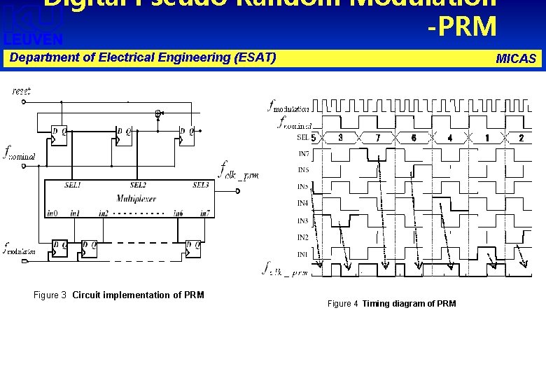
Digital Pseudo Random Modulation -PRM Department of Electrical Engineering (ESAT) Figure 3 Circuit implementation of PRM MICAS Figure 4 Timing diagram of PRM

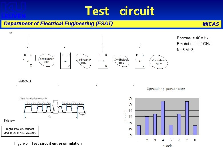
Test circuit Department of Electrical Engineering (ESAT) MICAS Fnominal = 40 MHz Fmodulation = 1 GHz N=3, M=8 Figure 5 Test circuit under simulation

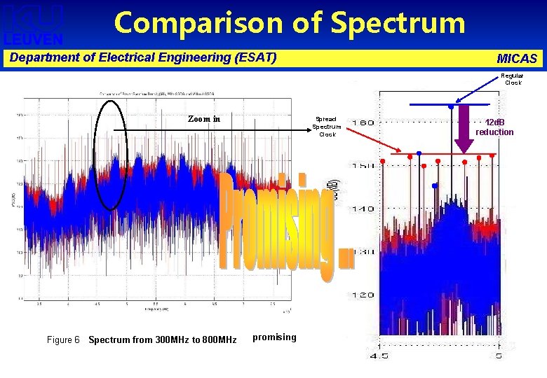
Comparison of Spectrum Department of Electrical Engineering (ESAT) MICAS Regular Clock Zoom in Figure 6 Spectrum from 300 MHz to 800 MHz Spread Spectrum Clock promising 12 d. B reduction