What is NANO What is NANO In 1960

- Slides: 82

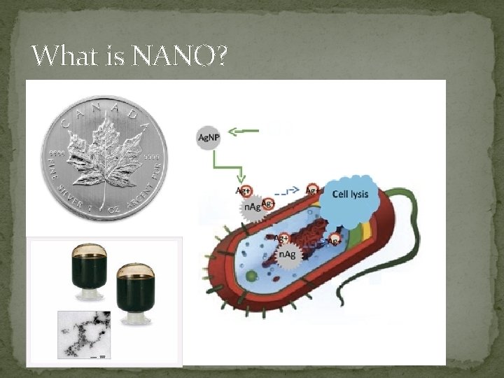
What is NANO?

What is NANO? �In 1960, the U. S. National Bureau of Standards adopted the prefix "nano-" for "a billionth". �Millimicrometer (millimicron) �mµ �µµ

What is NANO?

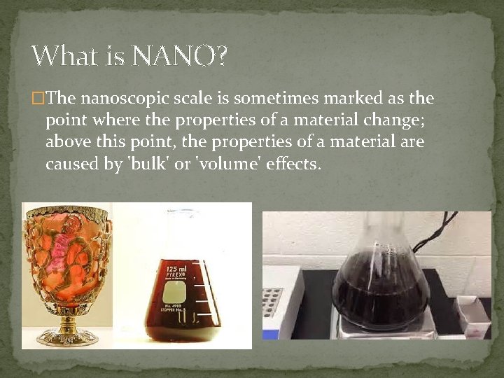
What is NANO? �The nanoscopic scale is sometimes marked as the point where the properties of a material change; above this point, the properties of a material are caused by 'bulk' or 'volume' effects.

What is NANO?

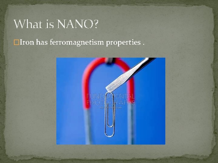
What is NANO? �Iron has ferromagnetism properties.

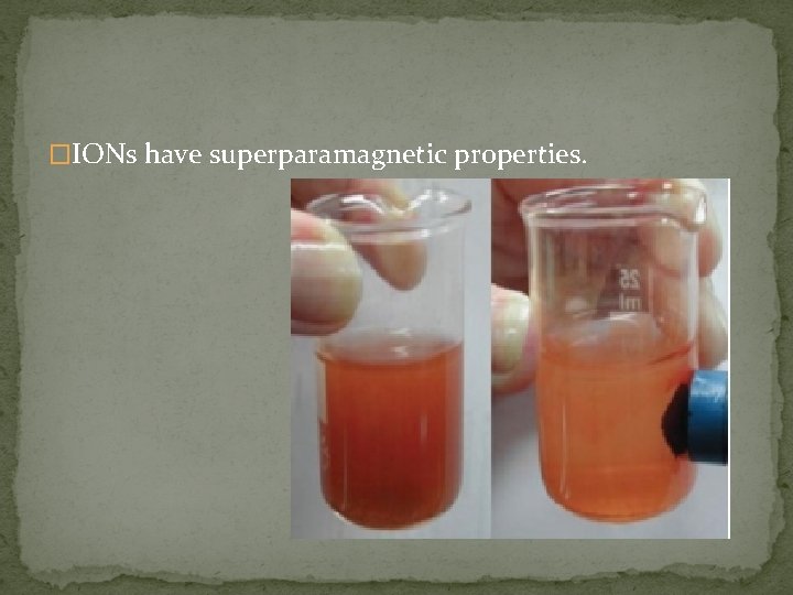
�IONs have superparamagnetic properties.

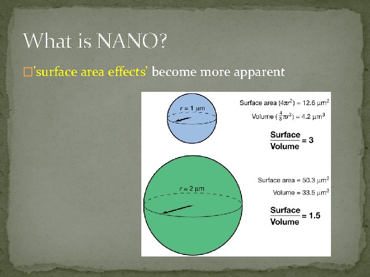
What is NANO? �'surface area effects' become more apparent

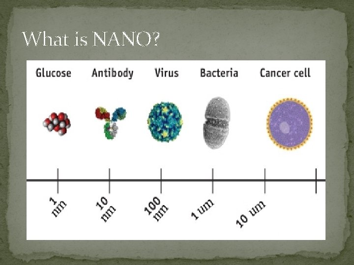
What is Nano-Materials? �Matter with at least one dimension sized from 1 to 100 nanometres.

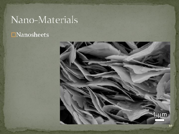
Nano-Materials �Nanosheets 10

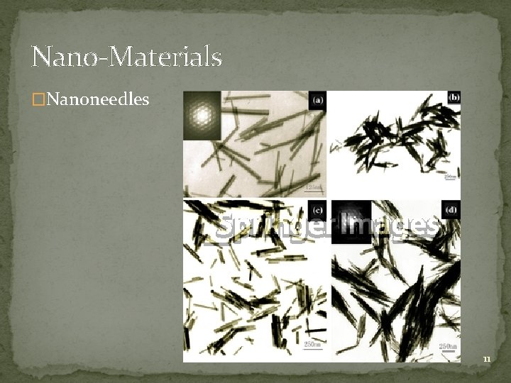
Nano-Materials �Nanoneedles 11

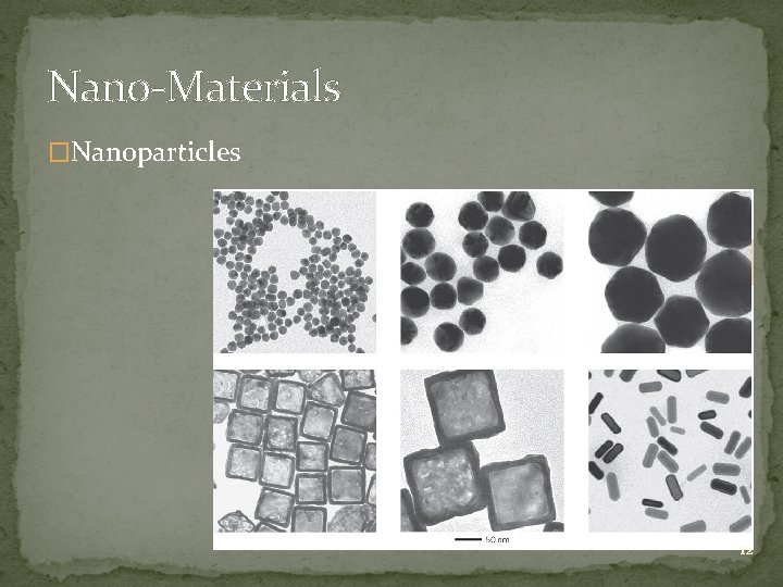
Nano-Materials �Nanoparticles 12

What is Nanotechnology? �National Nanotechnology Initiative (INN) Ø The manipulation of matter with at least one dimension sized from 1 to 100 nanometres.

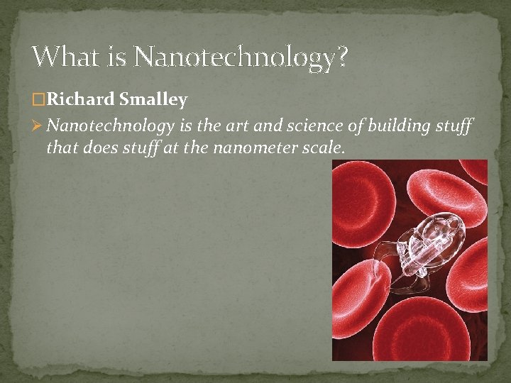
What is Nanotechnology? �Richard Smalley Ø Nanotechnology is the art and science of building stuff that does stuff at the nanometer scale.

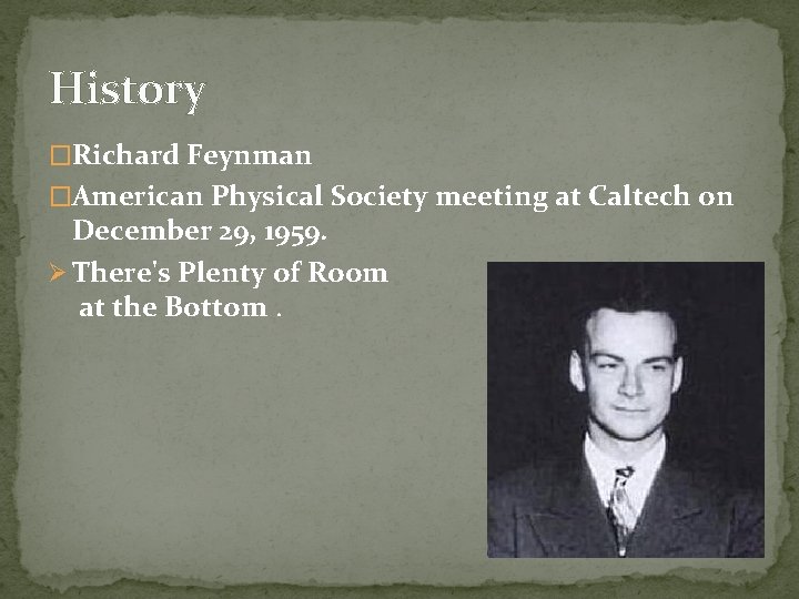
History �Richard Feynman �American Physical Society meeting at Caltech on December 29, 1959. Ø There's Plenty of Room at the Bottom.

History �Possibility of direct manipulation of individual atoms as a more powerful form of synthetic chemistry than those used at the time. �Molecular Nanotechnology

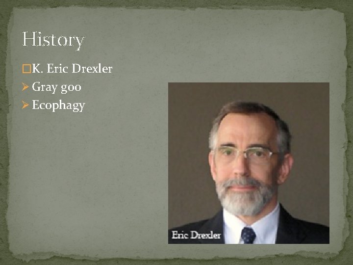
History �K. Eric Drexler Ø Gray goo Ø Ecophagy

History �Iran Nanotechnology Initiative Council (INIC)

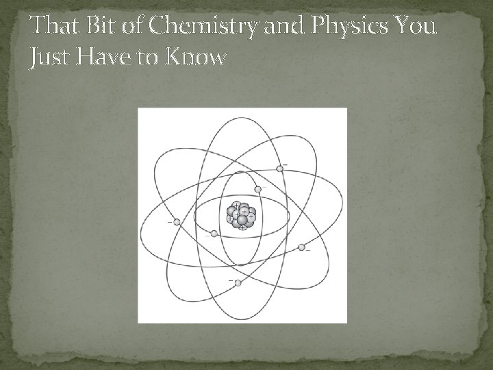
That Bit of Chemistry and Physics You Just Have to Know

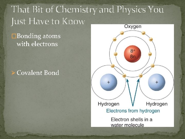
That Bit of Chemistry and Physics You Just Have to Know �Bonding atoms with electrons Ø Covalent Bond

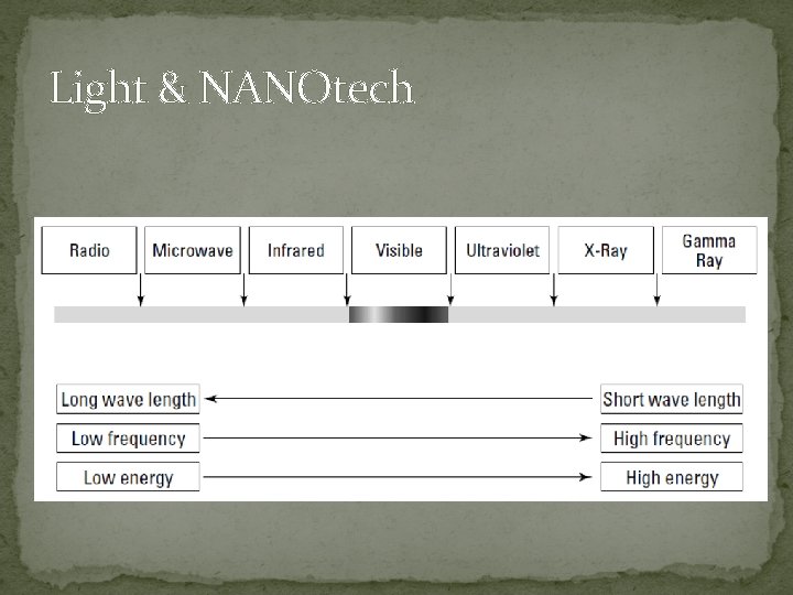
Turning on the light �Light & NANOtech

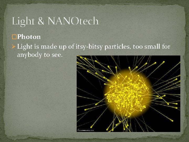
Light & NANOtech �Photon Ø Light is made up of itsy-bitsy particles, too small for anybody to see.

Light & NANOtech �Isaac Newton Ø light is essentially a stream of particles

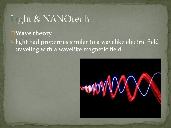
Light & NANOtech �Wave theory Ø light had properties similar to a wavelike electric field traveling with a wavelike magnetic field.

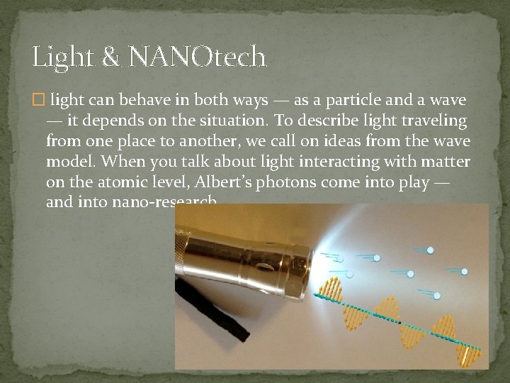
Light & NANOtech � light can behave in both ways — as a particle and a wave — it depends on the situation. To describe light traveling from one place to another, we call on ideas from the wave model. When you talk about light interacting with matter on the atomic level, Albert’s photons come into play — and into nano-research.

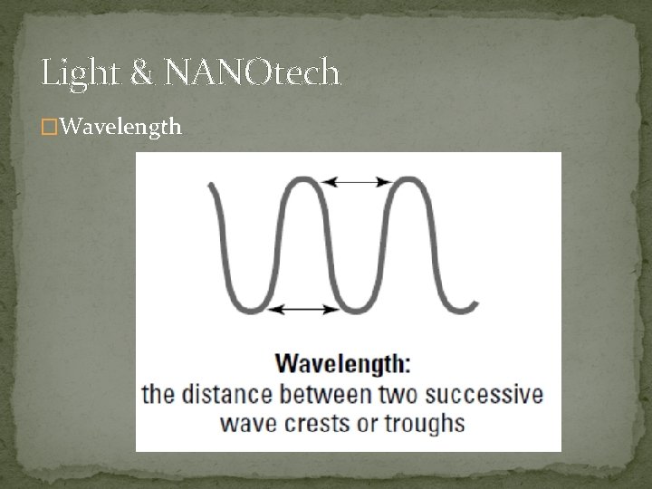
Light & NANOtech �Wavelength

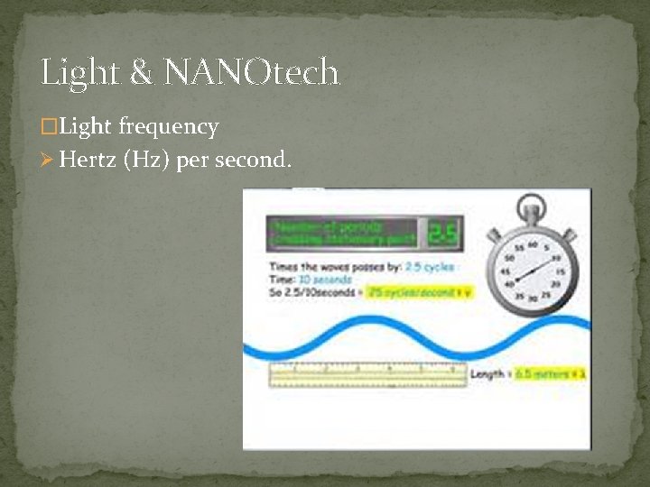
Light & NANOtech �Light frequency Ø Hertz (Hz) per second.

Light & NANOtech �C = f * λ �C (Light velocity): 299 792 458 metres per second ≈ 3 × 10⁸ m/s �f: frequency in cycles per second �λ: Wavelength in meter

Light & NANOtech

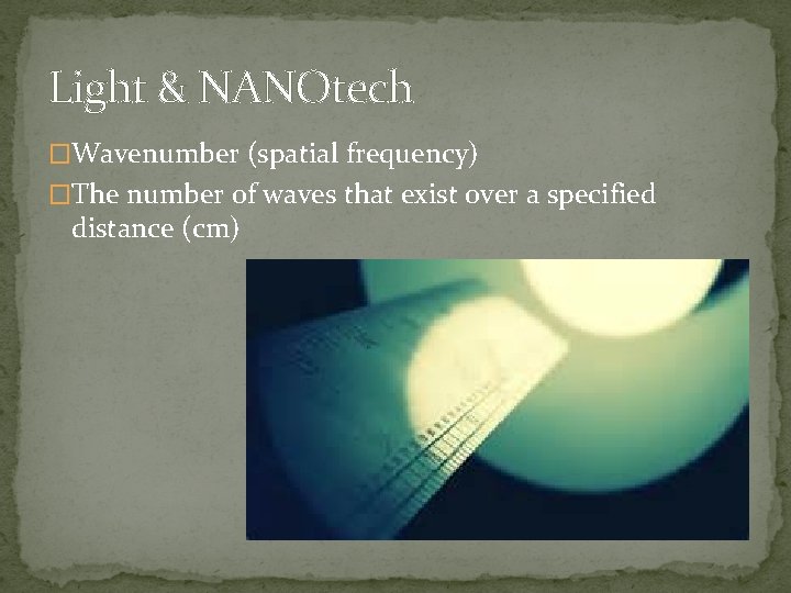
Light & NANOtech �Wavenumber (spatial frequency) �The number of waves that exist over a specified distance (cm)

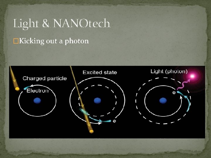
Light & NANOtech �Kicking out a photon

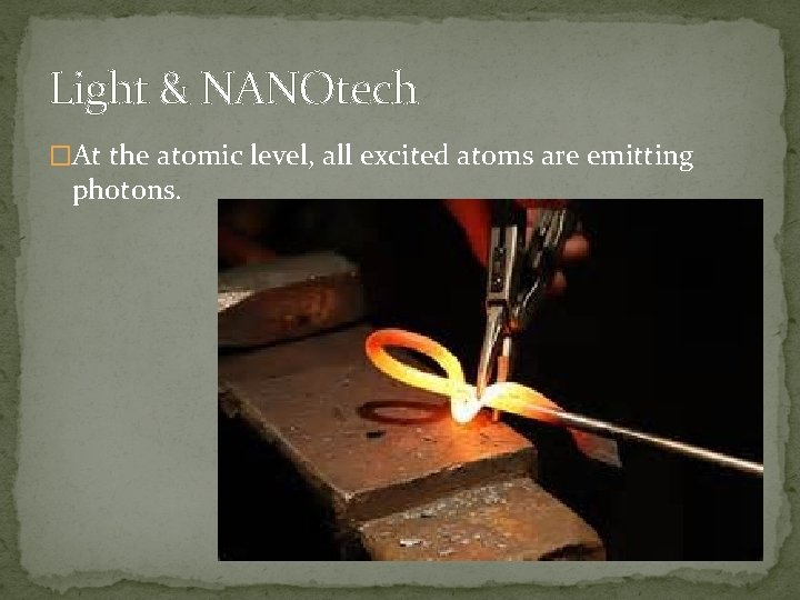
Light & NANOtech �At the atomic level, all excited atoms are emitting photons.

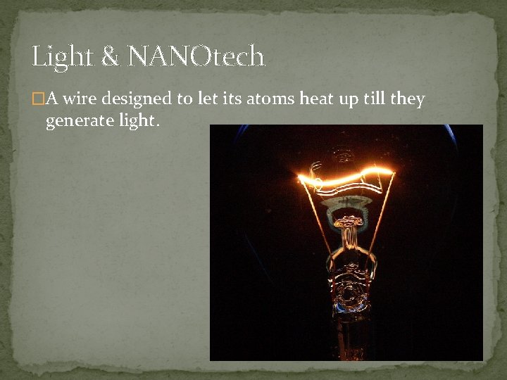
Light & NANOtech �A wire designed to let its atoms heat up till they generate light.

Light & NANOtech �Studying things that small requires special, deviously clever instruments that measure certain properties of matter — for example, spectrometers

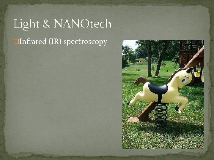
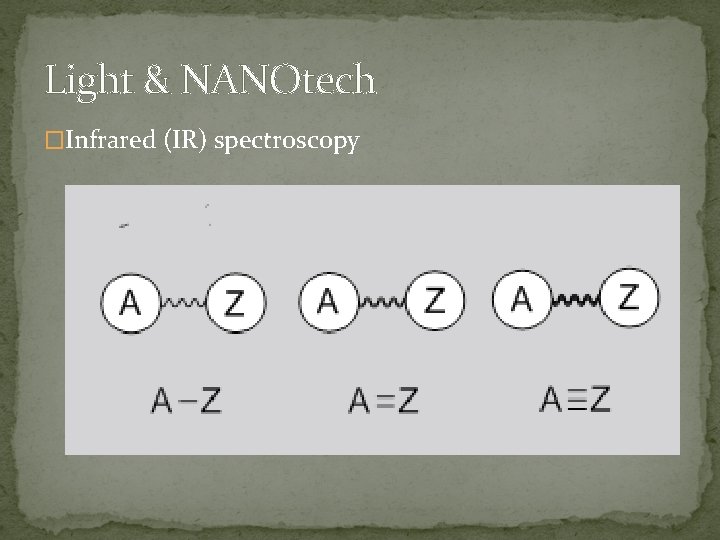
Light & NANOtech �Infrared (IR) spectroscopy

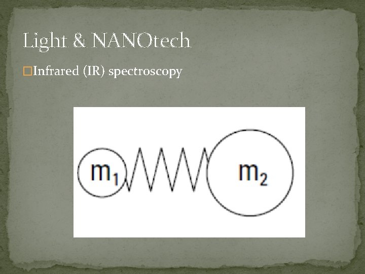
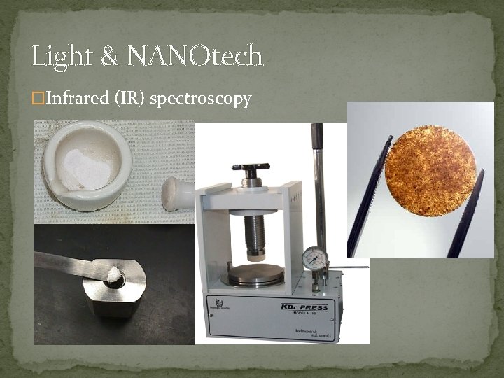
Light & NANOtech �Infrared (IR) spectroscopy

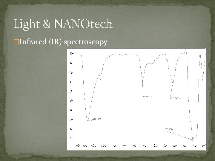
Light & NANOtech �Infrared (IR) spectroscopy

Light & NANOtech �Infrared (IR) spectroscopy

Light & NANOtech �Infrared (IR) spectroscopy

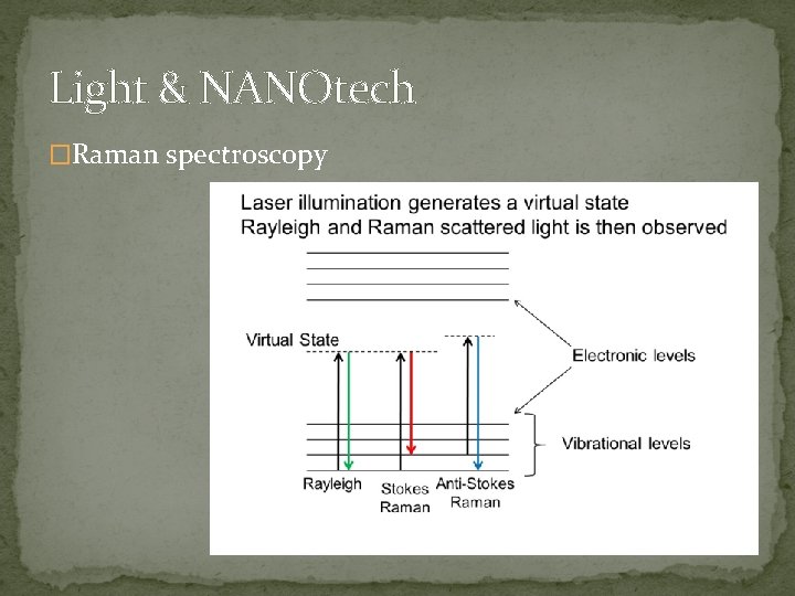
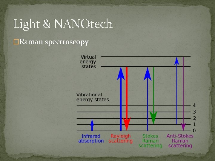
Light & NANOtech �Raman spectroscopy

Light & NANOtech �Raman spectroscopy

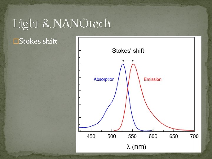
Light & NANOtech �Stokes shift

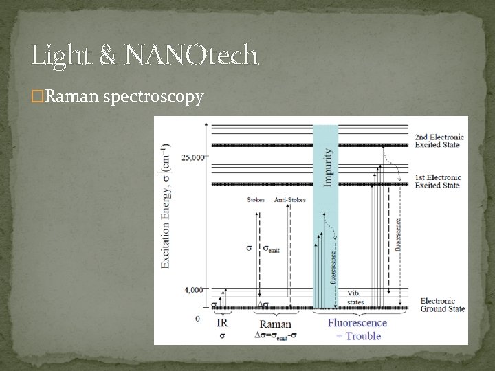
Light & NANOtech �Raman spectroscopy

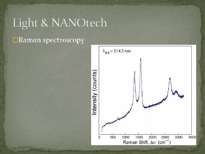
Light & NANOtech �Raman spectroscopy

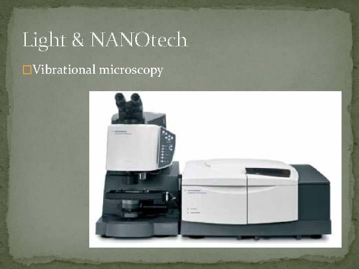
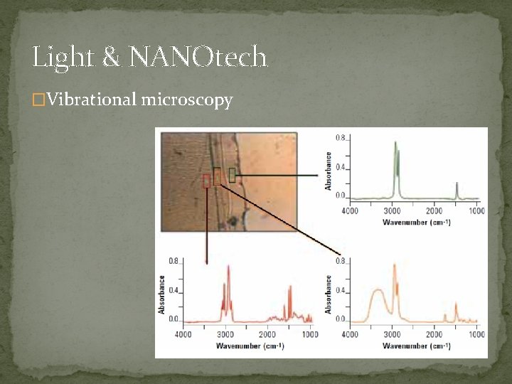
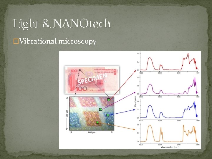
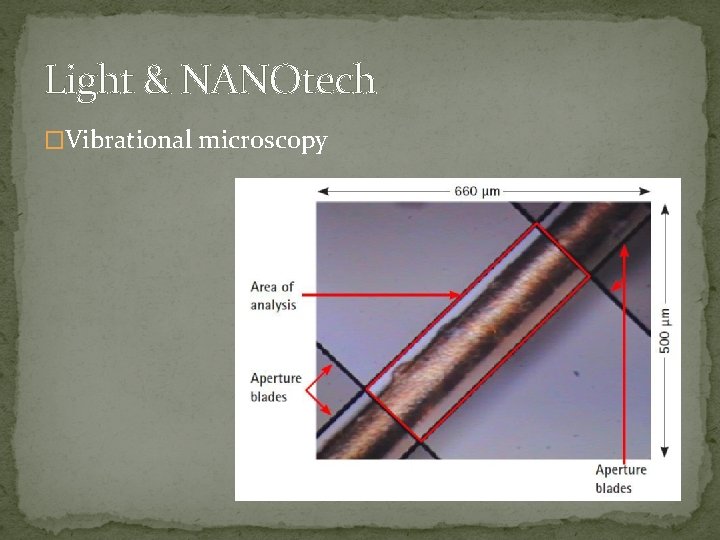
Light & NANOtech �Vibrational microscopy

Light & NANOtech �Vibrational microscopy

Light & NANOtech �Vibrational microscopy

Light & NANOtech �Vibrational microscopy

Vibrational microscopy �Applications in Biology and Medicine Ø Diseased tissue research Ø Identify chemical differences in plant leaf material Ø Identify bacteria using chemical imaging Ø Analysis of biomaterial interactions Ø Characterize ingredient or coating distribution in tablets Ø Identify counterfeit medications Ø Monitor solvent diffusion and active ingredient dissolution in blends or granules

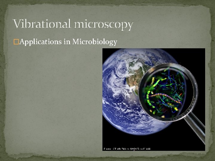
Vibrational microscopy �Applications in Microbiology

Light & NANOtech �Ultra Violet-Visible spectroscopy Ø The electrons in each type of atom can only absorb light of certain frequencies. Ø The spectrometer measures that frequency of light that passes through the sample.

Light & NANOtech • Ultra Violet-Visible spectroscopy Ø UV-Vis spectroscopy plays a role in the creation of nanosensors that can detect a material and identify its composition by bonding with it (also called capturing), which changes the nanosensor’s properties in specific ways that tell the tale.

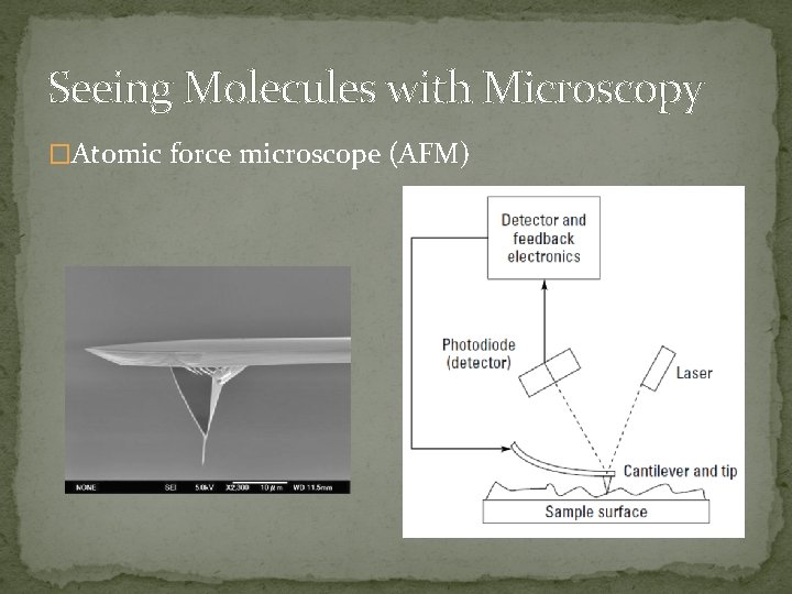
Seeing Molecules with Microscopy �Atomic force microscope (AFM)

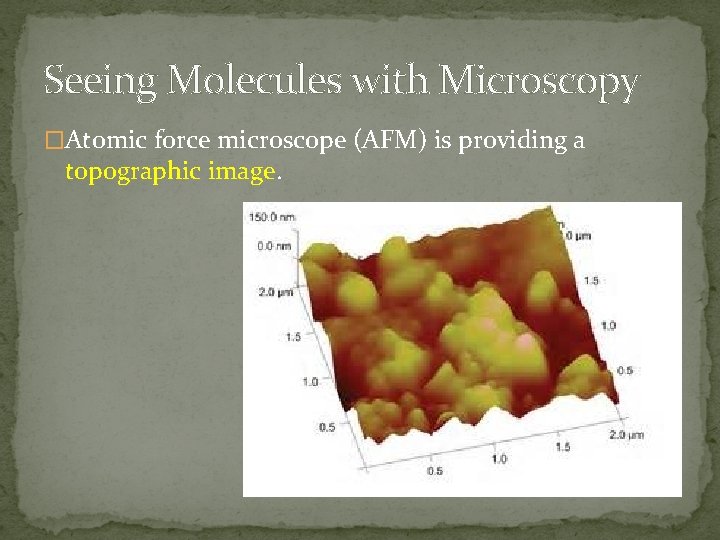
Seeing Molecules with Microscopy �Atomic force microscope (AFM) is providing a topographic image.

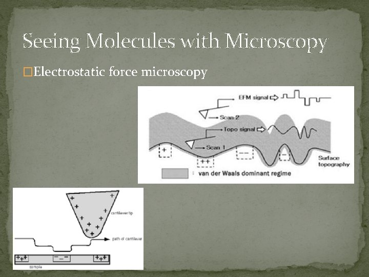
Seeing Molecules with Microscopy �Electrostatic force microscopy

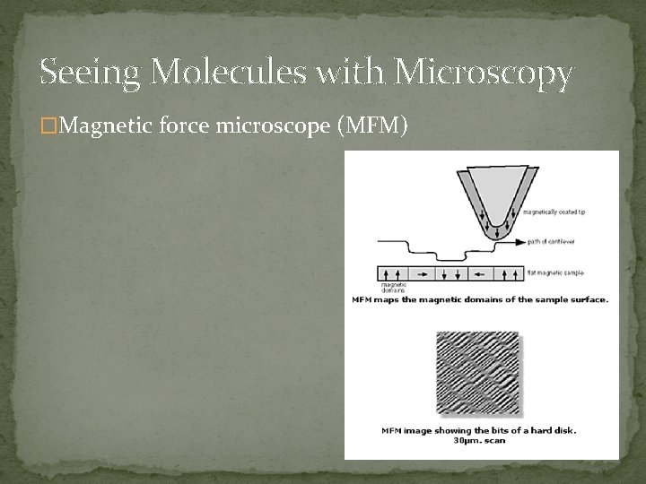
Seeing Molecules with Microscopy �Magnetic force microscope (MFM)

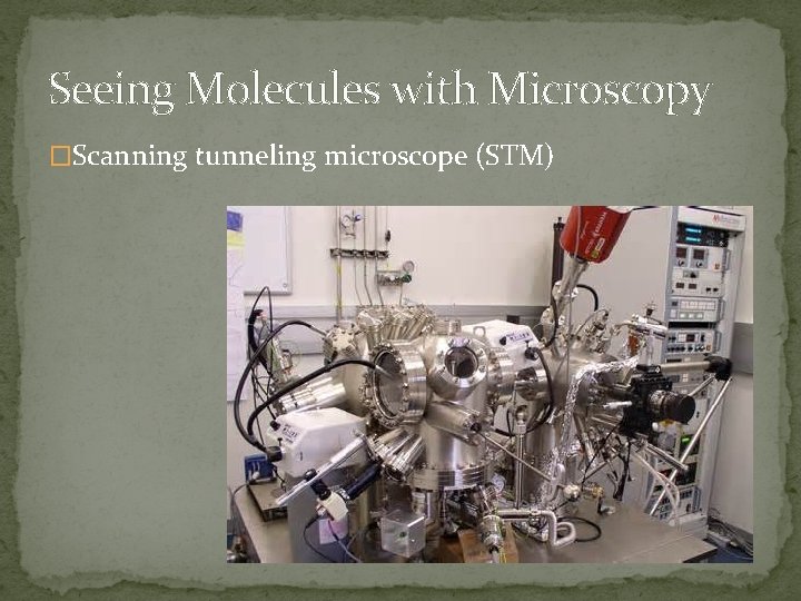
Seeing Molecules with Microscopy �Scanning tunneling microscope (STM)

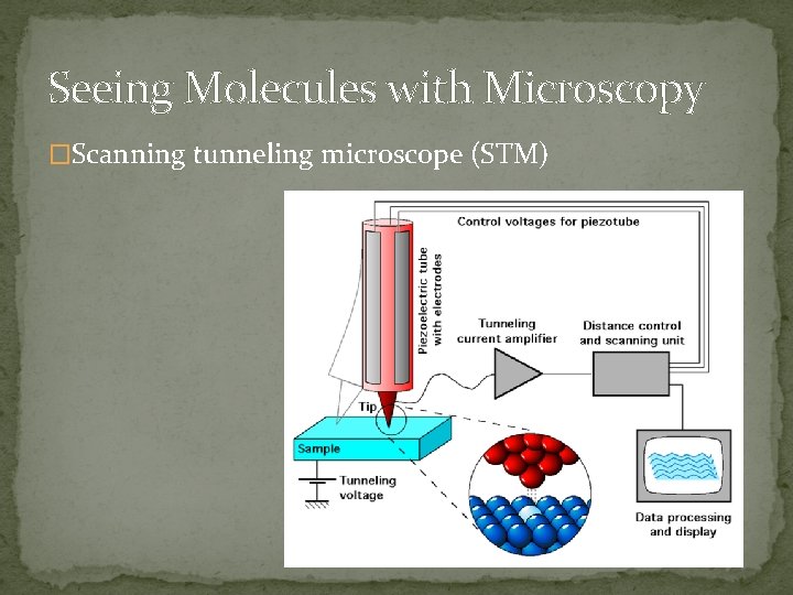
Seeing Molecules with Microscopy �Scanning tunneling microscope (STM)

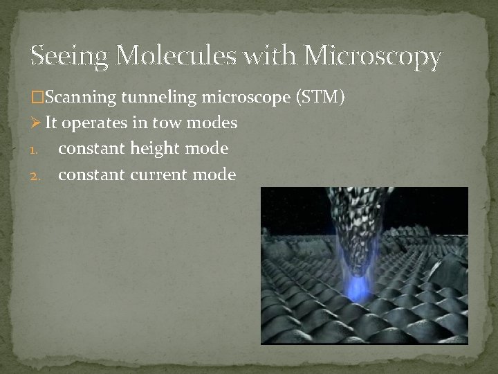
Seeing Molecules with Microscopy �Scanning tunneling microscope (STM) Ø It operates in tow modes constant height mode 2. constant current mode 1.

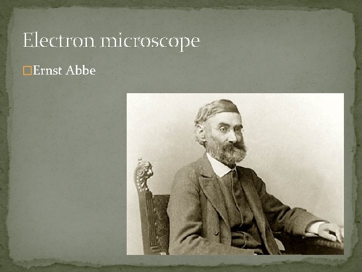
Electron microscope �Ernst Abbe

Ernst Abbe �The ability to resolve detail in an object was limited approximately by the wavelength of the light used in imaging, which limits the resolution of an optical microscope to a few hundred nanometers.

Köhler and Rohr �Developments into ultraviolet (UV) microscopes, led by Köhler and Rohr, allowed for an increase in resolving power of about a factor of two. �However this required more expensive quartz optical components, due to the absorption of UV by glass. �At this point it was believed that obtaining an image with sub-micrometre information was simply impossible due to this wavelength constraint.

Scanning electron microscope (SEM) �A wide range of magnifications is possible, from about 10 times (about equivalent to that of a powerful handlens) to more than 500, 000 times, about 250 times the magnification limit of the best light microscopes. �The types of signals produced by a SEM include secondary electrons (SE), back-scattered electrons (BSE), characteristic X-rays, light. �Secondary electron detectors are standard equipment in all SEMs, but it is rare that a single machine would have detectors for all possible signals.

Scanning electron microscope (SEM) �Back-scattered electrons (BSE) are beam electrons that are reflected from the sample by elastic scattering. �BSE are often used in analytical SEM along with the spectra made from the characteristic X-rays, because the intensity of the BSE signal is strongly related to the atomic number (Z) of the specimen. �BSE images can provide information about the distribution of different elements in the sample.

Scanning electron microscope (SEM) �Characteristic X-rays are emitted when the electron beam removes an inner shell electron from the sample, causing a higher-energy electron to fill the shell and release energy.

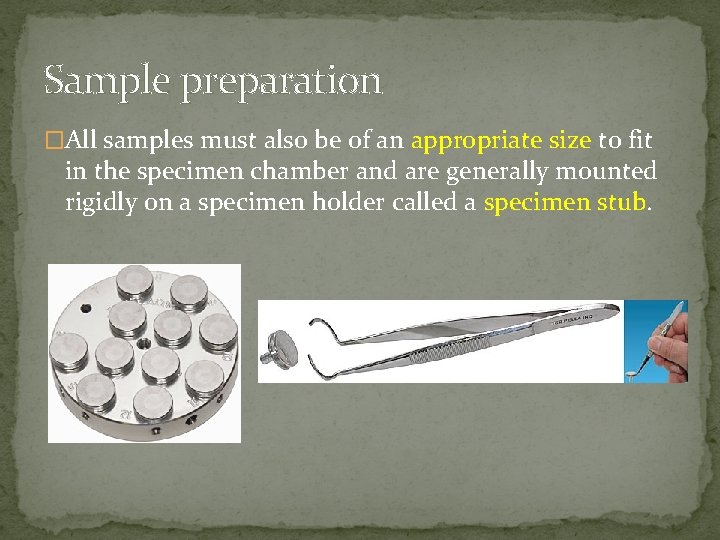
Sample preparation �All samples must also be of an appropriate size to fit in the specimen chamber and are generally mounted rigidly on a specimen holder called a specimen stub.

Sample preparation �For conventional imaging in the SEM, specimens must be electrically conductive, at least at the surface, and electrically grounded to prevent the accumulation of electrostatic charge at the surface.

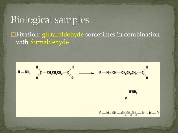
Biological samples �Fixation: glutaraldehyde sometimes in combination with formaldehyde

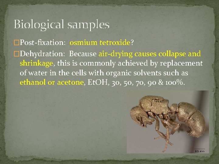
Biological samples �Post-fixation: osmium tetroxide? �Dehydration: Because air-drying causes collapse and shrinkage, this is commonly achieved by replacement of water in the cells with organic solvents such as ethanol or acetone, Et. OH, 30, 50, 70, 90 & 100%.

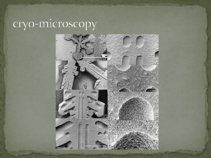
cryo-microscopy Ø Temperature-sensitive materials such as ice �Cryo-fixation �Cryo-stage �Low-temperature scanning electron microscopy

cryo-microscopy

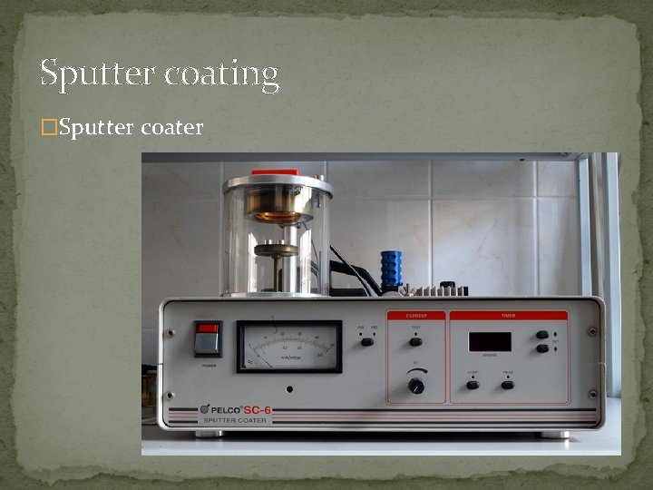
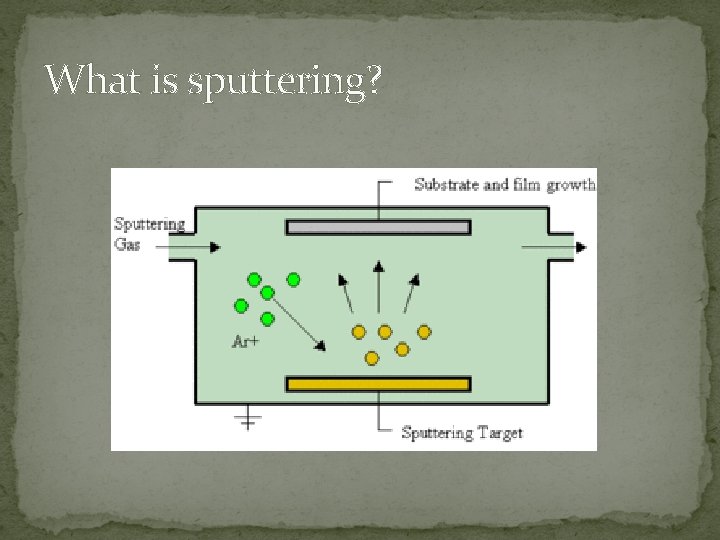
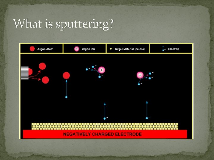
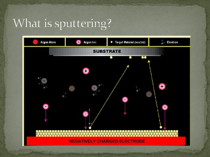
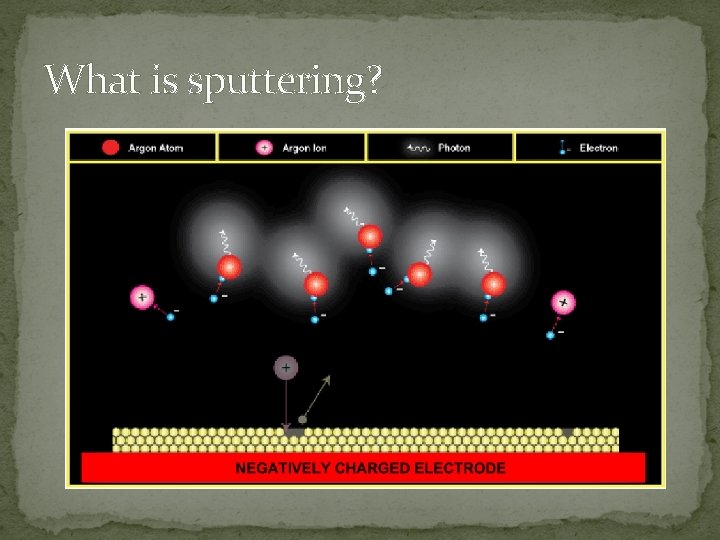
Sputter coating �Sputter coater

What is sputtering?

What is sputtering?

What is sputtering?

What is sputtering?

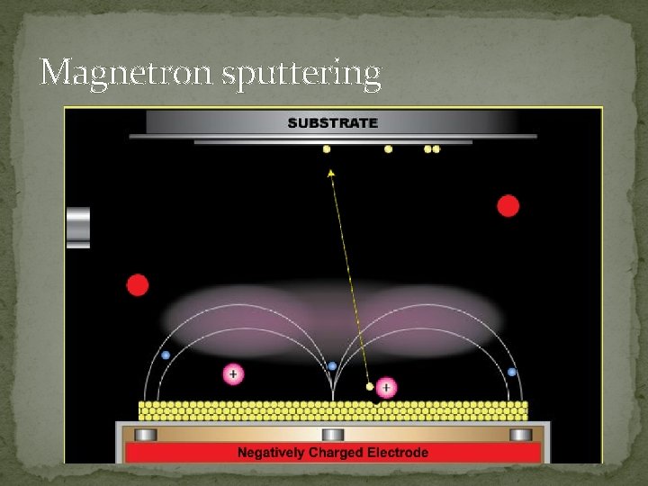
Magnetron sputtering

Magnification �Higher magnification results from reducing the size of the raster on the specimen

SEM �Topography: surface features such as texture �Morphology: shape, size, and arrangements of the particles that compose the object’s surface �Composition: elements that make up the sample (This can be determined by measuring the X-rays produced when the electron beam hits the sample. )

Transmission electron microscope (TEM) �Bouncing electrons off a sample is only one technique; you can also shoot electrons through �It’s a kind of nanoscale slide projector: Instead of shining a light through a photographic image (which allows certain parts of the light through), the TEM sends a beam of electrons through a sample.

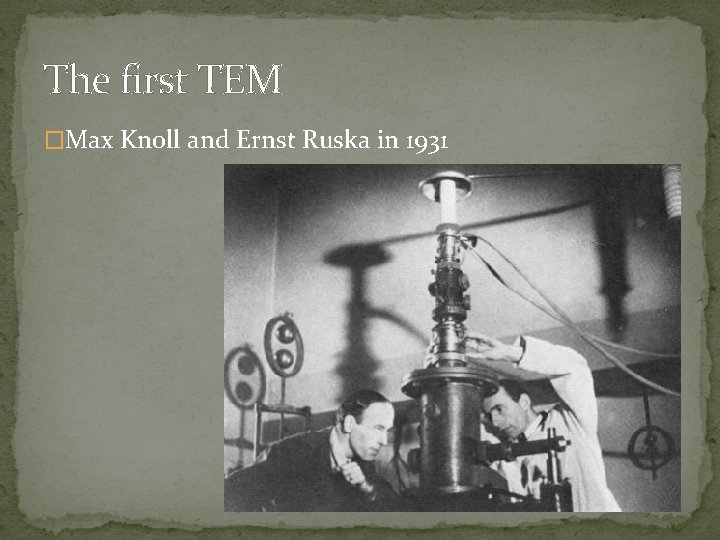
The first TEM �Max Knoll and Ernst Ruska in 1931
