Timing Diagram MCA 1 ST YEAR 2 ND



- Slides: 35
Timing Diagram MCA 1 ST YEAR 2 ND SEMESTER Paper No. MCA-203 Paper name: Microprocessor Dr. Utpal Nandi Dept. of Computer Science VIDYASAGAR UNIVERSITY
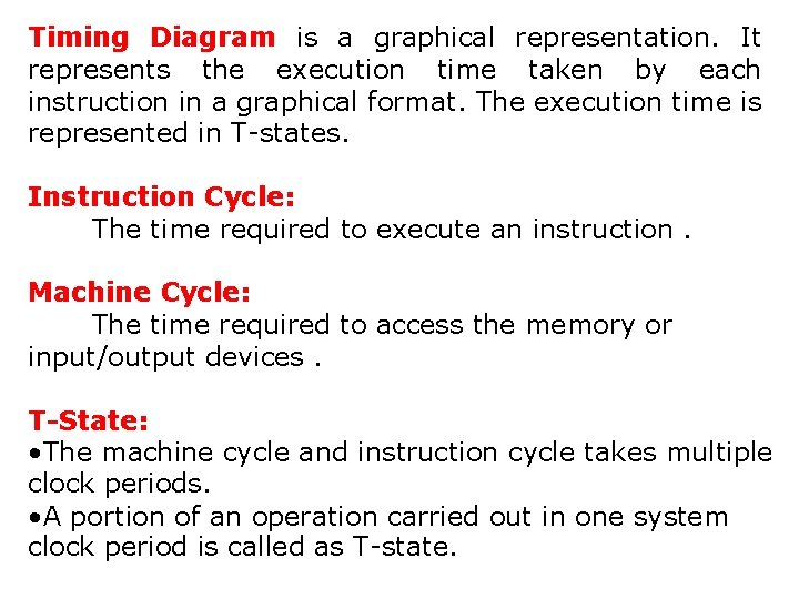
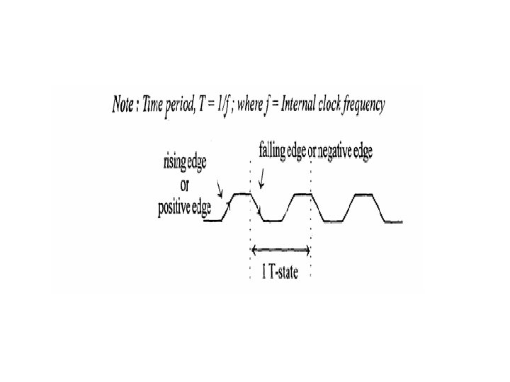
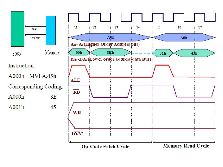
Timing Diagram is a graphical representation. It represents the execution time taken by each instruction in a graphical format. The execution time is represented in T-states. Instruction Cycle: The time required to execute an instruction. Machine Cycle: The time required to access the memory or input/output devices. T-State: • The machine cycle and instruction cycle takes multiple clock periods. • A portion of an operation carried out in one system clock period is called as T-state.
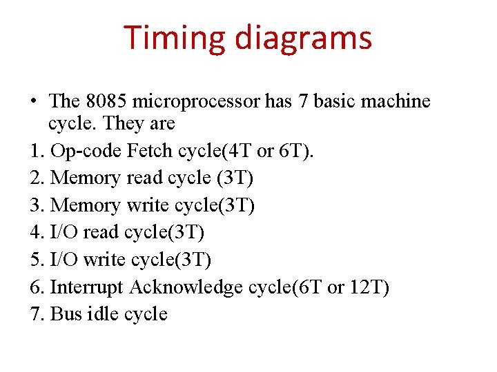
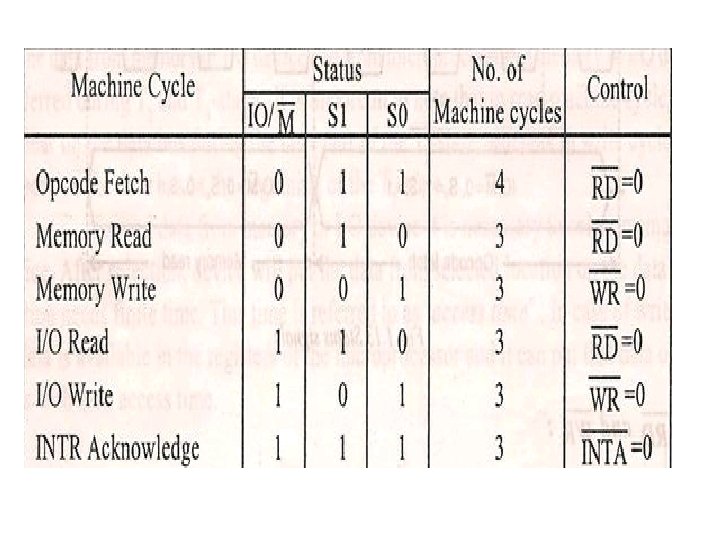
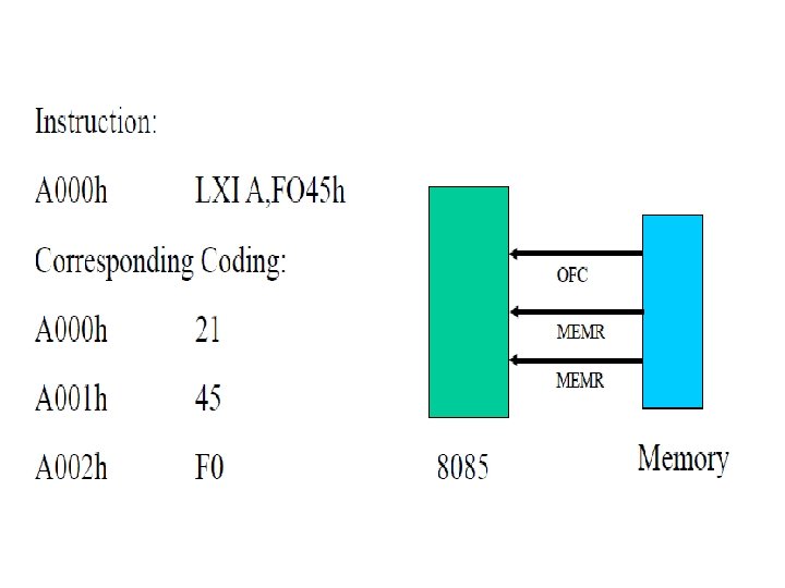
Timing diagrams • The 8085 microprocessor has 7 basic machine cycle. They are 1. Op-code Fetch cycle(4 T or 6 T). 2. Memory read cycle (3 T) 3. Memory write cycle(3 T) 4. I/O read cycle(3 T) 5. I/O write cycle(3 T) 6. Interrupt Acknowledge cycle(6 T or 12 T) 7. Bus idle cycle
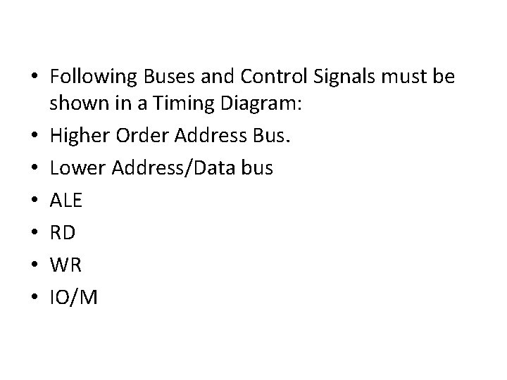
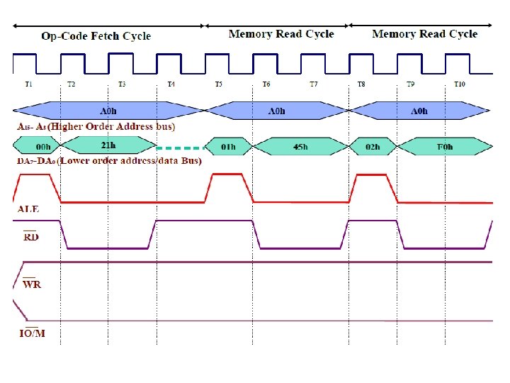
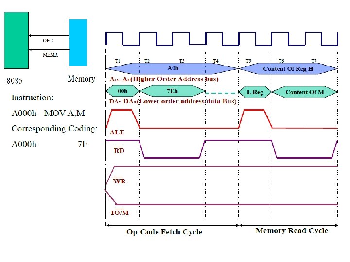
• Following Buses and Control Signals must be shown in a Timing Diagram: • Higher Order Address Bus. • Lower Address/Data bus • ALE • RD • WR • IO/M
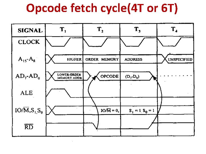
Opcode fetch cycle(4 T or 6 T)
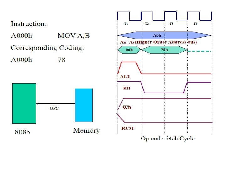
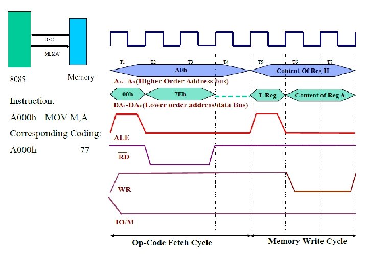
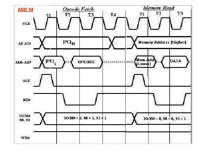
Opcode Fetch • The Opcode fetch cycle, fetches the instructions from memory and delivers it to the instruction register of the microprocessor • Opcode fetch machine cycle consists of 4 T-states. T 1 State: During the T 1 state, the contents of the program counter are placed on the 16 bit address bus. The higher order 8 bits are transferred to address bus (A 8 -A 15) and lower order 8 bits are transferred to multiplexed A/D (AD 0 -AD 7) bus. ALE (address latch enable) signal goes high. As soon as ALE goes high, the memory latches the AD 0 -AD 7 bus. At the middle of the T state the ALE goes low
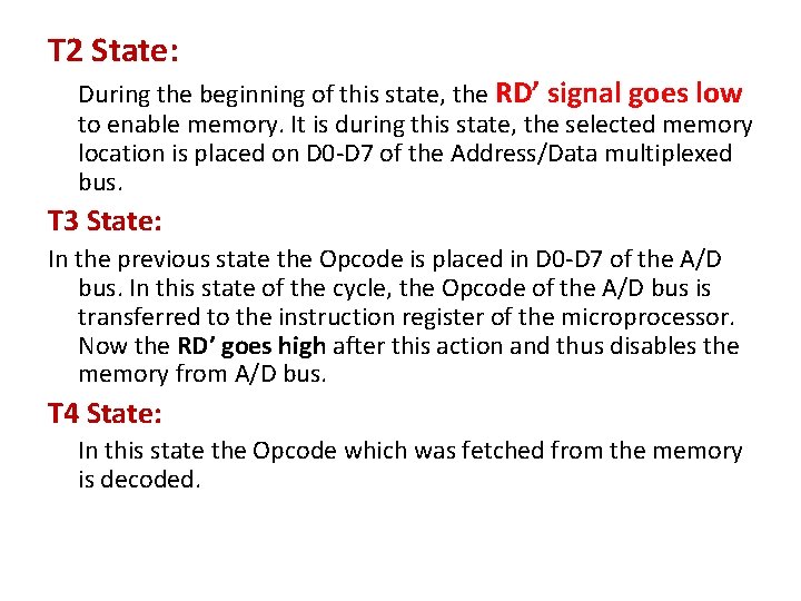
T 2 State: During the beginning of this state, the RD’ signal goes low to enable memory. It is during this state, the selected memory location is placed on D 0 -D 7 of the Address/Data multiplexed bus. T 3 State: In the previous state the Opcode is placed in D 0 -D 7 of the A/D bus. In this state of the cycle, the Opcode of the A/D bus is transferred to the instruction register of the microprocessor. Now the RD’ goes high after this action and thus disables the memory from A/D bus. T 4 State: In this state the Opcode which was fetched from the memory is decoded.
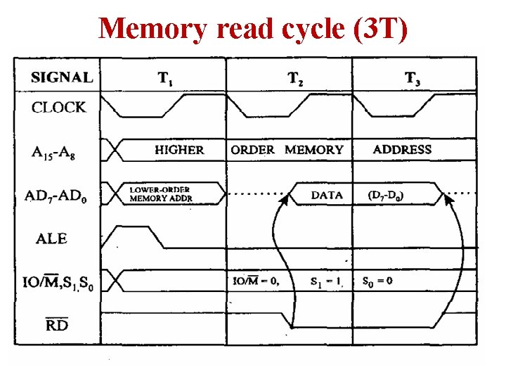
Memory read cycle (3 T)
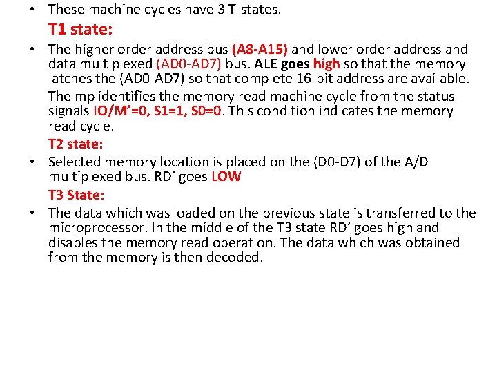
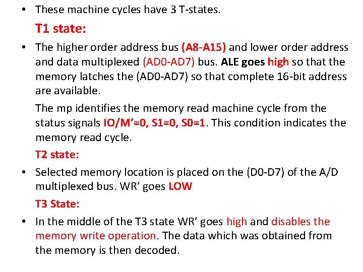
• These machine cycles have 3 T-states. T 1 state: • The higher order address bus (A 8 -A 15) and lower order address and data multiplexed (AD 0 -AD 7) bus. ALE goes high so that the memory latches the (AD 0 -AD 7) so that complete 16 -bit address are available. The mp identifies the memory read machine cycle from the status signals IO/M’=0, S 1=1, S 0=0. This condition indicates the memory read cycle. T 2 state: • Selected memory location is placed on the (D 0 -D 7) of the A/D multiplexed bus. RD’ goes LOW T 3 State: • The data which was loaded on the previous state is transferred to the microprocessor. In the middle of the T 3 state RD’ goes high and disables the memory read operation. The data which was obtained from the memory is then decoded.
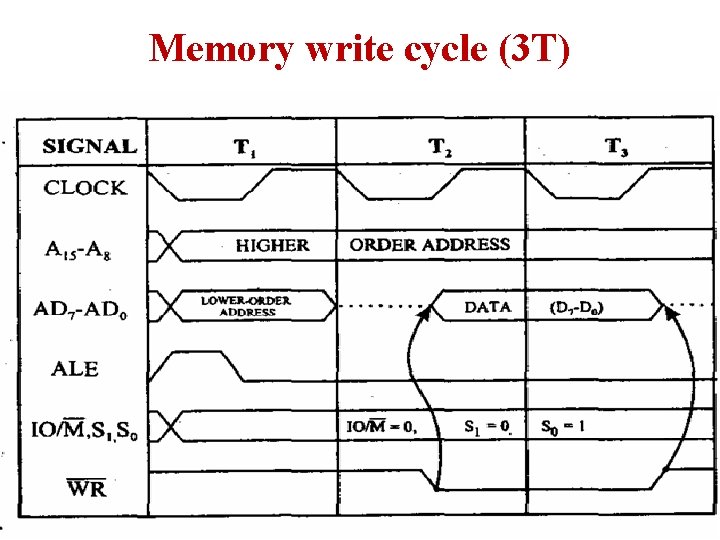
Memory write cycle (3 T)
• These machine cycles have 3 T-states. T 1 state: • The higher order address bus (A 8 -A 15) and lower order address and data multiplexed (AD 0 -AD 7) bus. ALE goes high so that the memory latches the (AD 0 -AD 7) so that complete 16 -bit address are available. The mp identifies the memory read machine cycle from the status signals IO/M’=0, S 1=0, S 0=1. This condition indicates the memory read cycle. T 2 state: • Selected memory location is placed on the (D 0 -D 7) of the A/D multiplexed bus. WR’ goes LOW T 3 State: • In the middle of the T 3 state WR’ goes high and disables the memory write operation. The data which was obtained from the memory is then decoded.
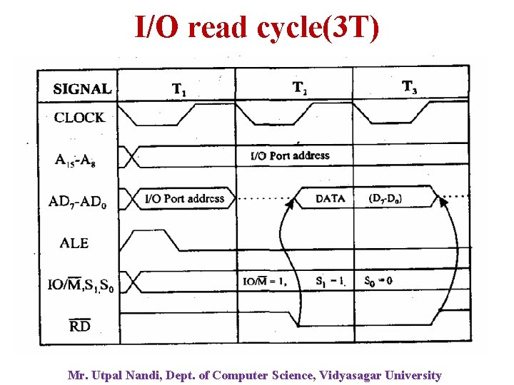
I/O read cycle(3 T) Mr. Utpal Nandi, Dept. of Computer Science, Vidyasagar University
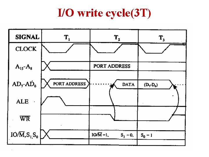
I/O write cycle(3 T)
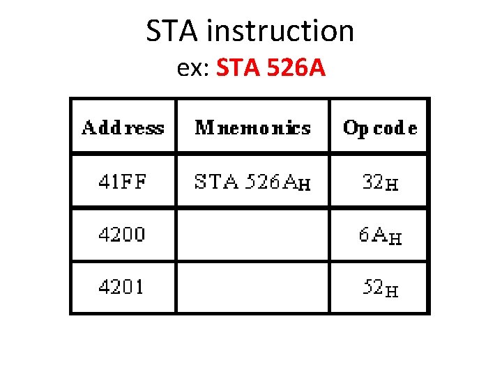
STA instruction ex: STA 526 A
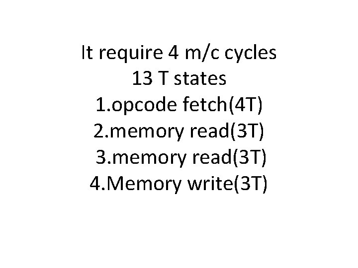
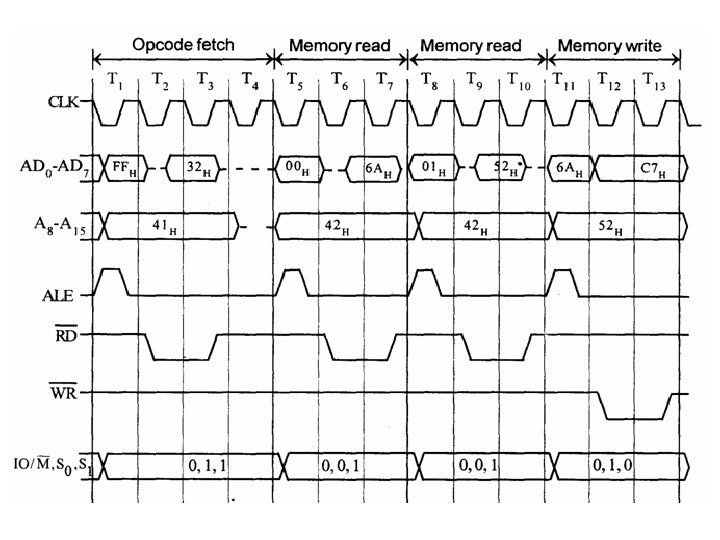
It require 4 m/c cycles 13 T states 1. opcode fetch(4 T) 2. memory read(3 T) 3. memory read(3 T) 4. Memory write(3 T)
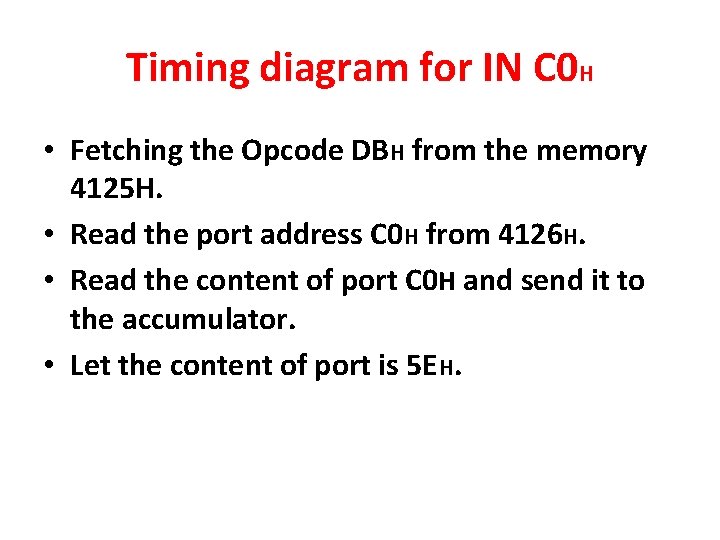
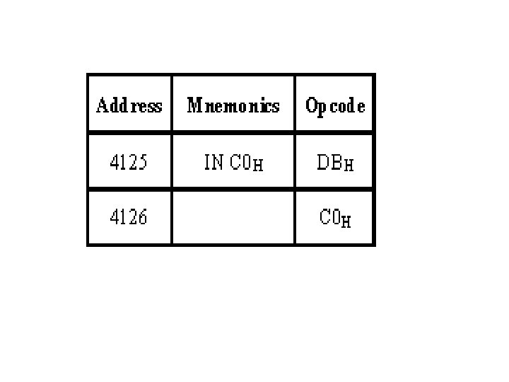
Timing diagram for IN C 0 H • Fetching the Opcode DBH from the memory 4125 H. • Read the port address C 0 H from 4126 H. • Read the content of port C 0 H and send it to the accumulator. • Let the content of port is 5 EH.
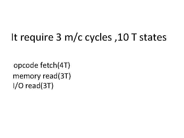
It require 3 m/c cycles , 10 T states opcode fetch(4 T) memory read(3 T) I/O read(3 T)
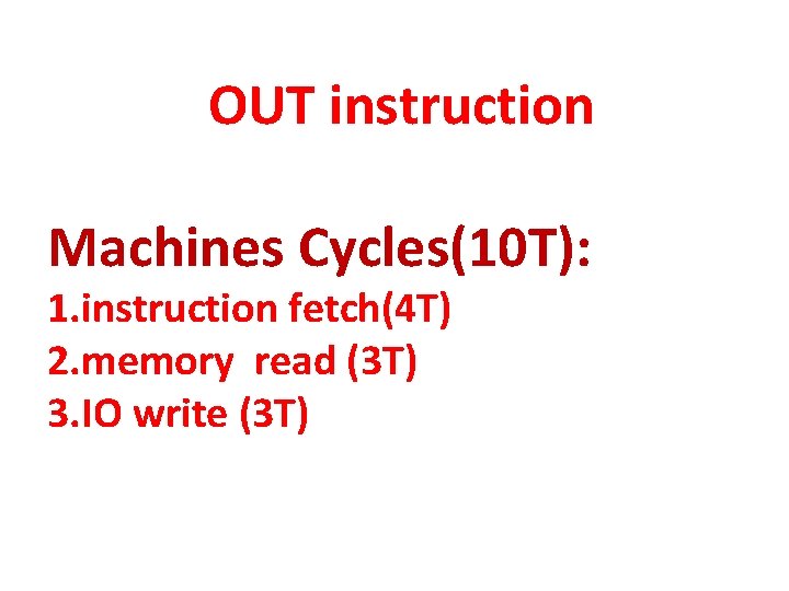
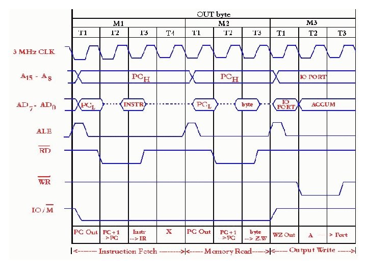
OUT instruction Machines Cycles(10 T): 1. instruction fetch(4 T) 2. memory read (3 T) 3. IO write (3 T)
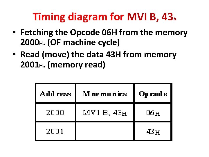
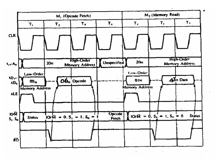
Timing diagram for MVI B, 43 h • Fetching the Opcode 06 H from the memory 2000 H. (OF machine cycle) • Read (move) the data 43 H from memory 2001 H. (memory read)
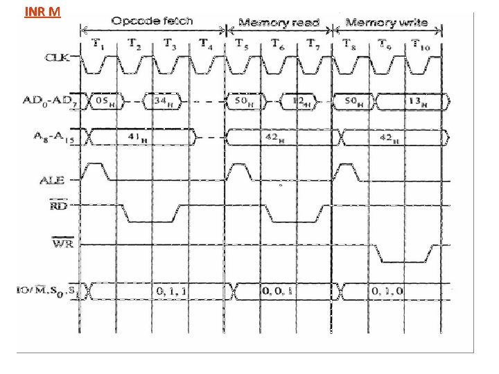
INR M
ADD M
End