Silicon Detectors for Tracking and Vertexing Andrei Nomerotski


- Slides: 55

Silicon Detectors for Tracking and Vertexing Andrei Nomerotski, University of Oxford INSTR 08, Novosibirsk 29 February 2008 1 Andrei Nomerotski

Silicon Detectors · Using silicon diode as s detector u 1951: first observation of signals in reversely biased p-n junction from a’s · Development for tracking stimulated by need to measure short-lived charm/beauty quarks and tau lepton in ’ 70 · 1980, J. Kemmer: first proposed to use planar process developed in industry to produce strip silicon detectors u u Fast, localized charge deposition 3 micron intrinsic resolution Planar process dimensions precise to 1 micron, low cost 2 Andrei Nomerotski

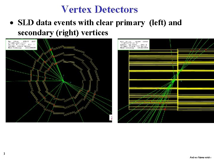
Vertex Detectors · SLD data events with clear primary (left) and secondary (right) vertices 3 Andrei Nomerotski

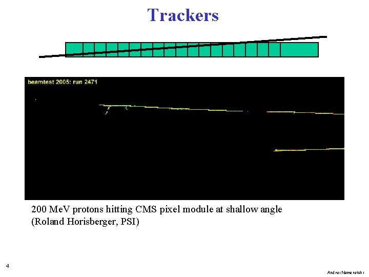
Trackers 200 Me. V protons hitting CMS pixel module at shallow angle (Roland Horisberger, PSI) 4 Andrei Nomerotski

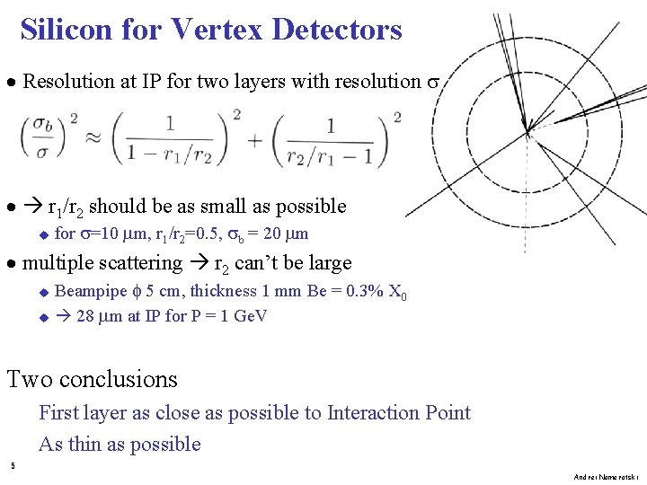
Silicon for Vertex Detectors · Resolution at IP for two layers with resolution s · r 1/r 2 should be as small as possible u for s=10 mm, r 1/r 2=0. 5, sb = 20 mm · multiple scattering r 2 can’t be large Beampipe f 5 cm, thickness 1 mm Be = 0. 3% X 0 u 28 mm at IP for P = 1 Ge. V u Two conclusions First layer as close as possible to Interaction Point As thin as possible 5 Andrei Nomerotski

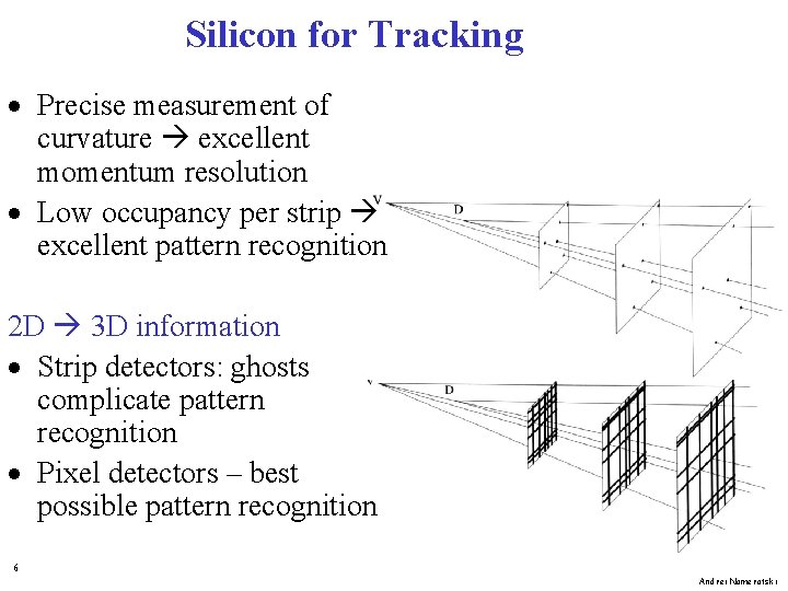
Silicon for Tracking · Precise measurement of curvature excellent momentum resolution · Low occupancy per strip excellent pattern recognition 2 D 3 D information · Strip detectors: ghosts complicate pattern recognition · Pixel detectors – best possible pattern recognition 6 Andrei Nomerotski

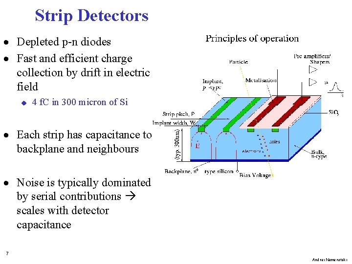
Strip Detectors · Depleted p-n diodes · Fast and efficient charge collection by drift in electric field u 4 f. C in 300 micron of Si · Each strip has capacitance to backplane and neighbours · Noise is typically dominated by serial contributions scales with detector capacitance 7 Andrei Nomerotski

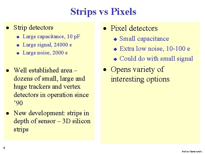
Strips vs Pixels · Strip detectors u u u Large capacitance, 10 p. F Large signal, 24000 e Large noise, 2000 e · Pixel detectors u u u · Well established area – dozens of small, large and huge trackers and vertex detectors in operation since ’ 90 · New development: strips in depth of sensor – 3 D silicon strips Small capacitance Extra low noise, 10 -100 e Could do with small signal · Opens variety of interesting options 8 Andrei Nomerotski

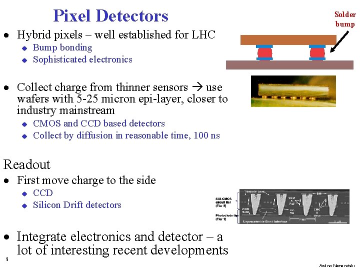
Pixel Detectors · Hybrid pixels – well established for LHC u u Solder bump Bump bonding Sophisticated electronics · Collect charge from thinner sensors use wafers with 5 -25 micron epi-layer, closer to industry mainstream u u CMOS and CCD based detectors Collect by diffusion in reasonable time, 100 ns Readout · First move charge to the side u u CCD Silicon Drift detectors · Integrate electronics and detector – a lot of interesting recent developments 9 Andrei Nomerotski

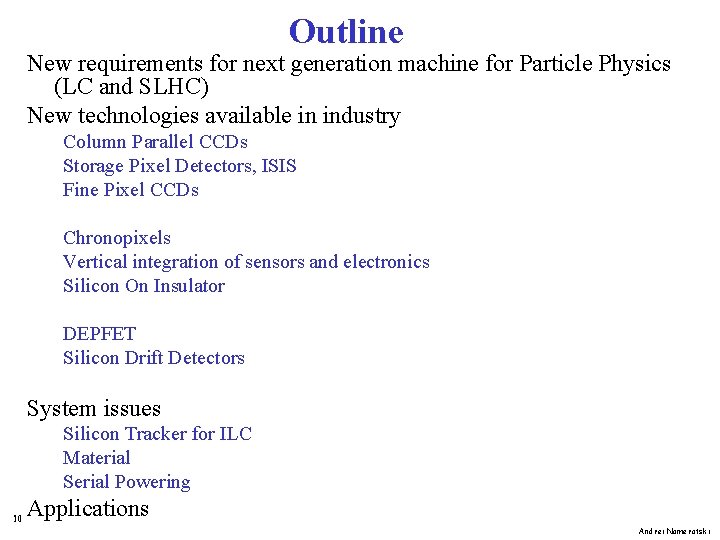
Outline New requirements for next generation machine for Particle Physics (LC and SLHC) New technologies available in industry Column Parallel CCDs Storage Pixel Detectors, ISIS Fine Pixel CCDs Chronopixels Vertical integration of sensors and electronics Silicon On Insulator DEPFET Silicon Drift Detectors System issues Silicon Tracker for ILC Material Serial Powering 10 Applications Andrei Nomerotski

I will not discuss in this talk : · Active Pixel Sensors (APS) u Talk by Lars Eklund · 3 D and active edge silicon u Talk by Daniel Pennicard · LHC and other existing trackers / vertex detectors u Multiple talks in this session · Radiation hardness issues u Review by Gianluigi Casse 11 Andrei Nomerotski

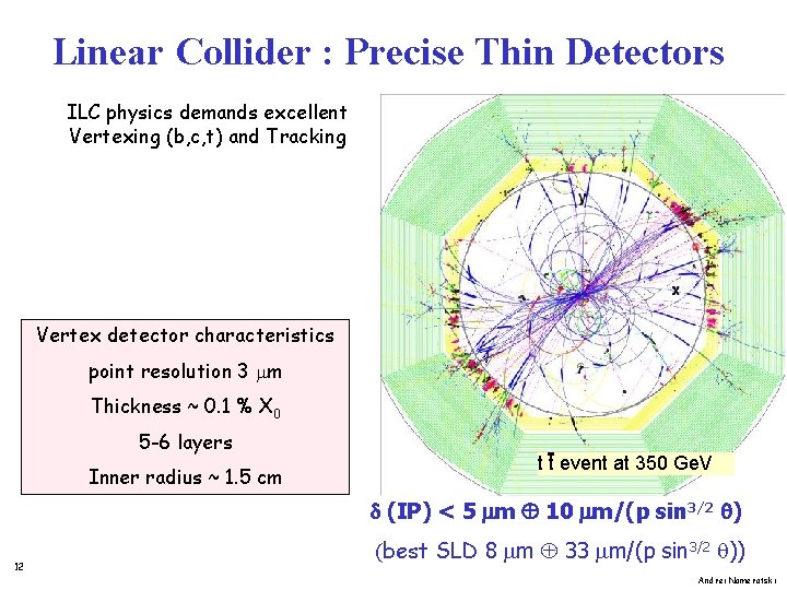
Linear Collider : Precise Thin Detectors ILC physics demands excellent Vertexing (b, c, t) and Tracking Vertex detector characteristics point resolution 3 mm Thickness ~ 0. 1 % X 0 5 -6 layers Inner radius ~ 1. 5 cm t t event at 350 Ge. V d (IP) < 5 m 10 m/(p sin 3/2 q) 12 (best SLD 8 mm 33 mm/(p sin 3/2 q)) Andrei Nomerotski

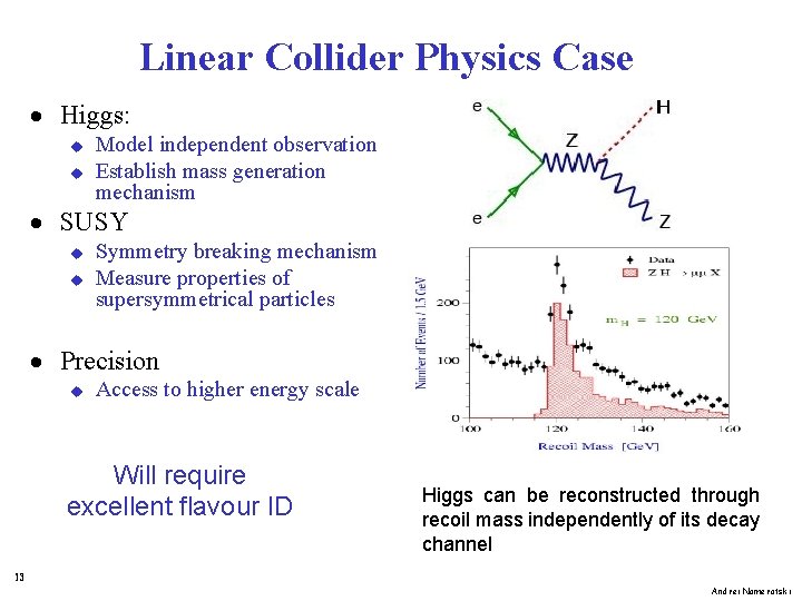
Linear Collider Physics Case · Higgs: u u Model independent observation Establish mass generation mechanism · SUSY u u Symmetry breaking mechanism Measure properties of supersymmetrical particles · Precision u Access to higher energy scale Will require excellent flavour ID Higgs can be reconstructed through recoil mass independently of its decay channel 13 Andrei Nomerotski

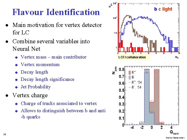
b c light Flavour Identification · Main motivation for vertex detector for LC · Combine several variables into Neural Net u u u Vertex mass – main contributor Vertex momentum Decay length significance Jet Probability LCFI collaboration · Vertex charge u u Charge of tracks associated to vertex Allows to distinguish between b and anti -b quarks 14 Andrei Nomerotski

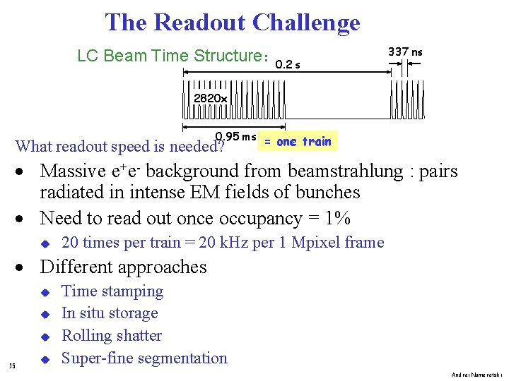
The Readout Challenge LC Beam Time Structure: 0. 2 s 337 ns 2820 x 0. 95 ms = one train What readout speed is needed? · Massive e+e- background from beamstrahlung : pairs radiated in intense EM fields of bunches · Need to read out once occupancy = 1% u 20 times per train = 20 k. Hz per 1 Mpixel frame · Different approaches u u u 15 u Time stamping In situ storage Rolling shatter Super-fine segmentation Andrei Nomerotski

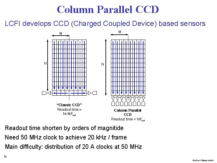
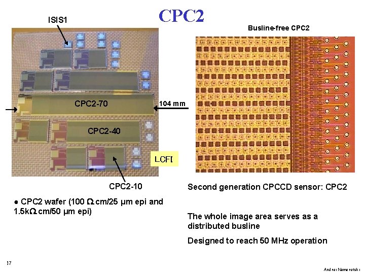
Column Parallel CCD LCFI develops CCD (Charged Coupled Device) based sensors M M N N “Classic CCD” Readout time N M/fout Column Parallel CCD Readout time = N/fout Readout time shorten by orders of magnitide Need 50 MHz clock to achieve 20 k. Hz / frame Main difficulty: distribution of 20 A clocks at 50 MHz 16 Andrei Nomerotski

CPC 2 ISIS 1 CPC 2 -70 Busline-free CPC 2 104 mm CPC 2 -40 LCFI CPC 2 -10 ● CPC 2 wafer (100 . cm/25 μm epi and 1. 5 k. cm/50 μm epi) Second generation CPCCD sensor: CPC 2 The whole image area serves as a distributed busline Designed to reach 50 MHz operation 17 Andrei Nomerotski

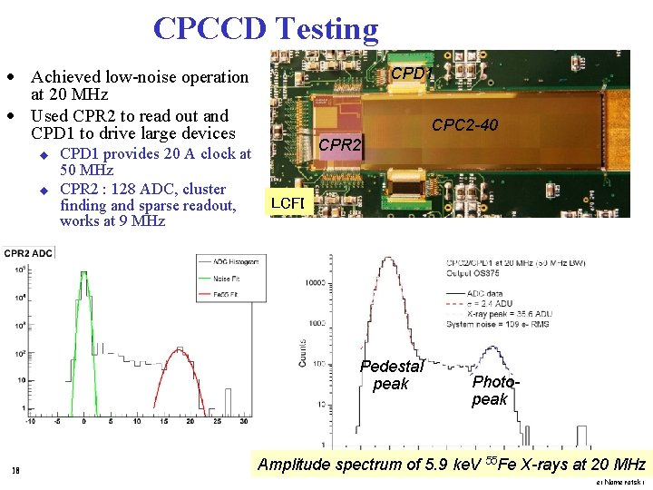
CPCCD Testing · Achieved low-noise operation at 20 MHz · Used CPR 2 to read out and CPD 1 to drive large devices u u CPD 1 provides 20 A clock at 50 MHz CPR 2 : 128 ADC, cluster finding and sparse readout, works at 9 MHz CPD 1 CPC 2 -40 CPR 2 LCFI Pedestal peak 18 Photopeak Amplitude spectrum of 5. 9 ke. V 55 Fe X-rays at 20 MHz Andrei Nomerotski

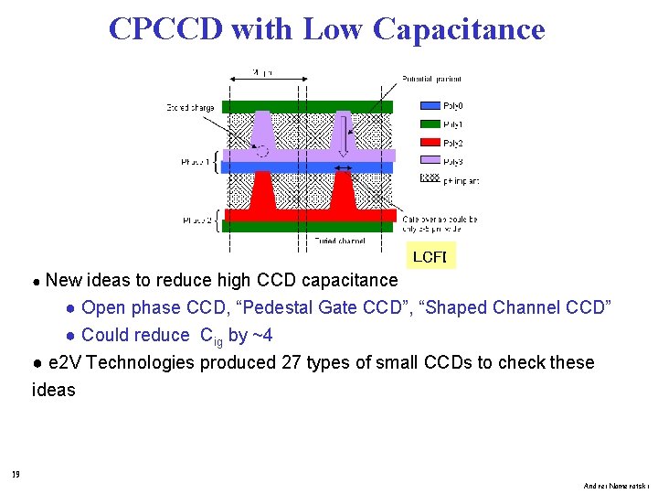
CPCCD with Low Capacitance LCFI ● New ideas to reduce high CCD capacitance ● Open phase CCD, “Pedestal Gate CCD”, “Shaped Channel CCD” ● Could reduce Cig by ~4 ● e 2 V Technologies produced 27 types of small CCDs to check these ideas 19 Andrei Nomerotski

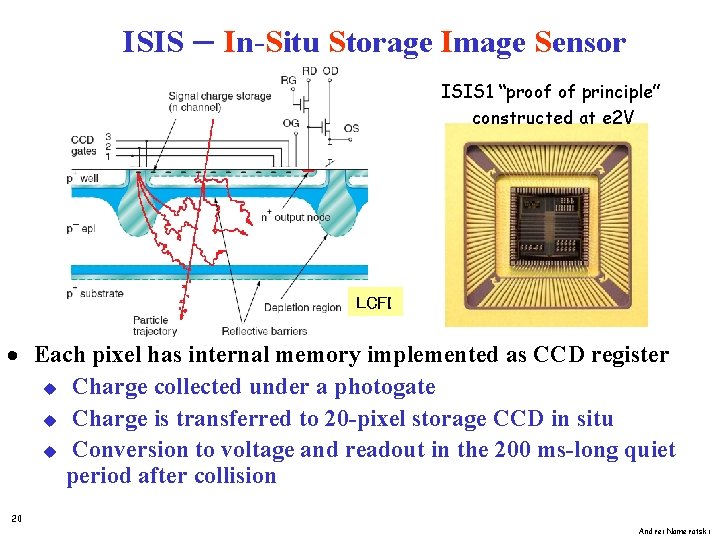
ISIS – In-Situ Storage Image Sensor ISIS 1 “proof of principle” constructed at e 2 V LCFI · Each pixel has internal memory implemented as CCD register u Charge collected under a photogate u Charge is transferred to 20 -pixel storage CCD in situ u Conversion to voltage and readout in the 200 ms-long quiet period after collision 20 Andrei Nomerotski

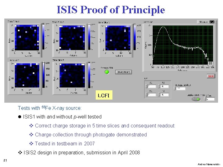
ISIS Proof of Principle LCFI Tests with 55 Fe X-ray source: l ISIS 1 with and without p-well tested v Correct charge storage in 5 time slices and consequent readout v Charge collection through photogate demonstrated v Tested in testbeam in 2007 v ISIS 2 design in preparation, submission in April 2008 21 Andrei Nomerotski

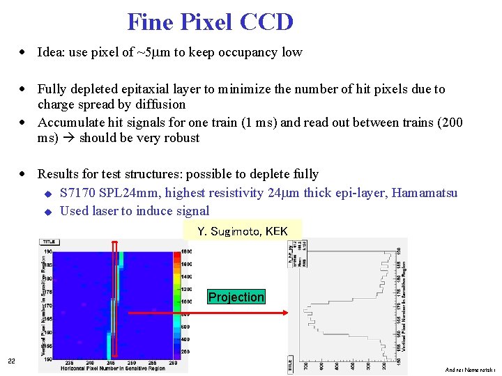
Fine Pixel CCD · Idea: use pixel of ~5 mm to keep occupancy low · Fully depleted epitaxial layer to minimize the number of hit pixels due to charge spread by diffusion · Accumulate hit signals for one train (1 ms) and read out between trains (200 ms) should be very robust · Results for test structures: possible to deplete fully u S 7170 SPL 24 mm, highest resistivity 24 mm thick epi-layer, Hamamatsu u Used laser to induce signal Y. Sugimoto, KEK Projection 22 Andrei Nomerotski

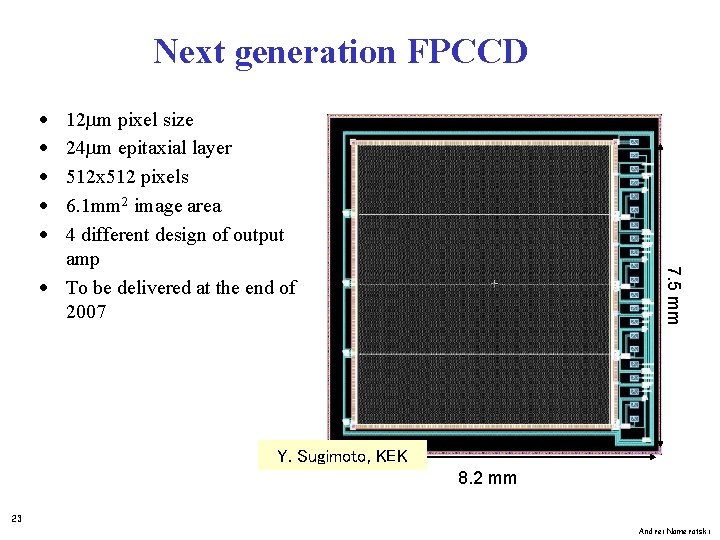
Next generation FPCCD · · · 7. 5 mm 12 mm pixel size 24 mm epitaxial layer 512 x 512 pixels 6. 1 mm 2 image area 4 different design of output amp · To be delivered at the end of 2007 Y. Sugimoto, KEK 8. 2 mm 23 Andrei Nomerotski

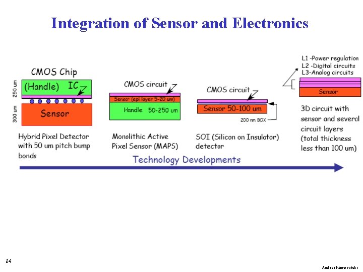
Integration of Sensor and Electronics 24 Andrei Nomerotski

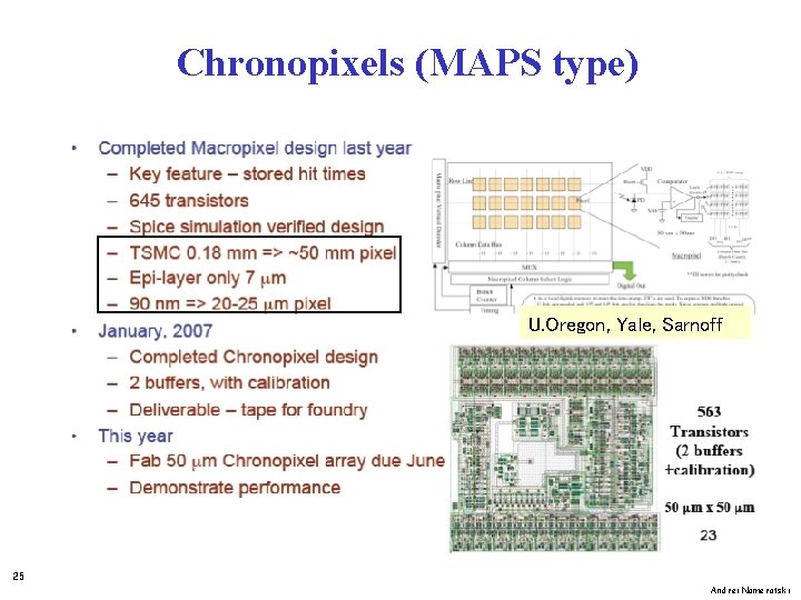
Chronopixels (MAPS type) U. Oregon, Yale, Sarnoff 25 Andrei Nomerotski

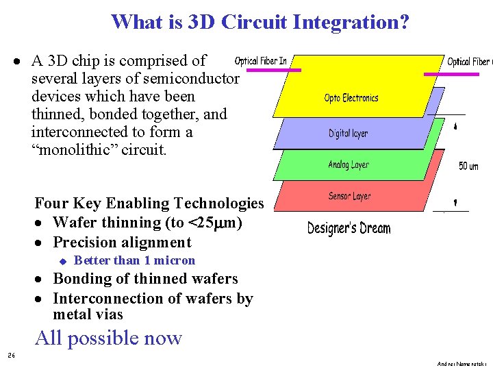
What is 3 D Circuit Integration? · A 3 D chip is comprised of several layers of semiconductor devices which have been thinned, bonded together, and interconnected to form a “monolithic” circuit. Four Key Enabling Technologies · Wafer thinning (to <25 m) · Precision alignment u Better than 1 micron · Bonding of thinned wafers · Interconnection of wafers by metal vias All possible now 26 Andrei Nomerotski

3 D Integration is Future Mainstream in Industry · Industry is moving toward 3 D to improve circuit performance. u u Reduce R, L, C for higher speed Reduce chip I/O pads Provide increased functionality Reduce interconnect power and crosstalk · Utilizes technology developed for Silicon-on-Insulator devices 27 Andrei Nomerotski

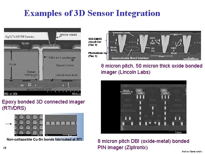
Examples of 3 D Sensor Integration 8 micron pitch, 50 micron thick oxide bonded imager (Lincoln Labs) Epoxy bonded 3 D connected imager (RTI/DRS) 28 8 micron pitch DBI (oxide-metal) bonded PIN imager (Ziptronix) Andrei Nomerotski

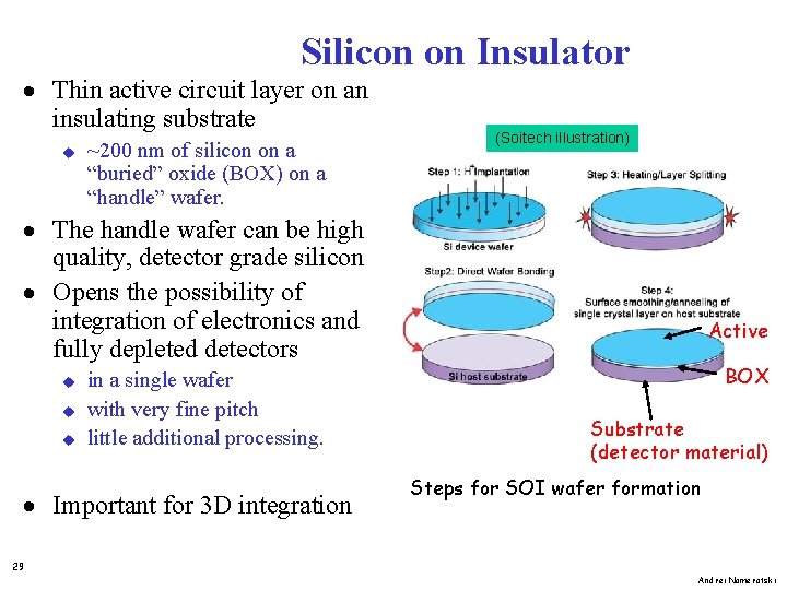
Silicon on Insulator · Thin active circuit layer on an insulating substrate u ~200 nm of silicon on a “buried” oxide (BOX) on a “handle” wafer. (Soitech illustration) · The handle wafer can be high quality, detector grade silicon · Opens the possibility of integration of electronics and fully depleted detectors u u u in a single wafer with very fine pitch little additional processing. · Important for 3 D integration Active BOX Substrate (detector material) Steps for SOI wafer formation 29 Andrei Nomerotski

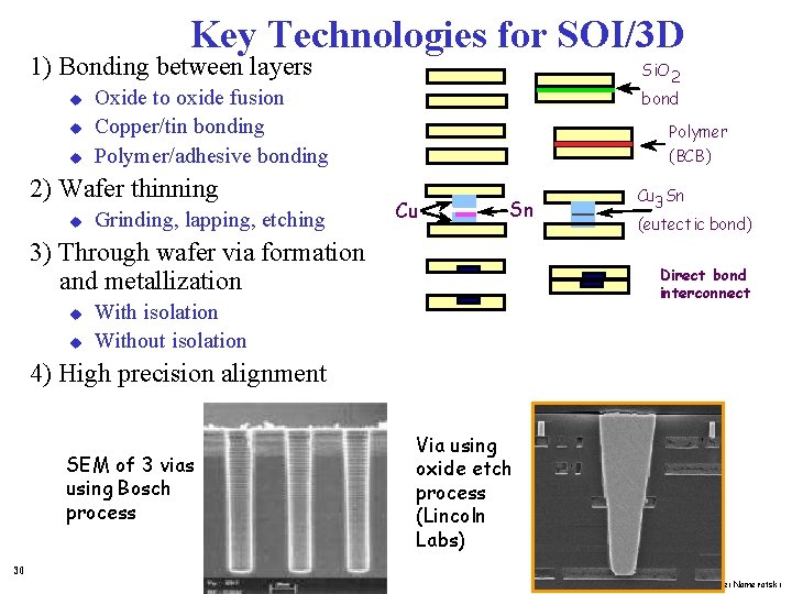
Key Technologies for SOI/3 D 1) Bonding between layers u u u Oxide to oxide fusion Copper/tin bonding Polymer/adhesive bonding 2) Wafer thinning u Si. O 2 Grinding, lapping, etching bond Polymer (BCB) Cu Sn 3) Through wafer via formation and metallization u u Cu 3 Sn (eutectic bond) Direct bond interconnect With isolation Without isolation 4) High precision alignment SEM of 3 vias using Bosch process Via using oxide etch process (Lincoln Labs) 30 Andrei Nomerotski

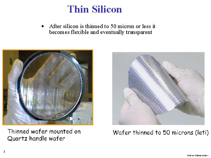
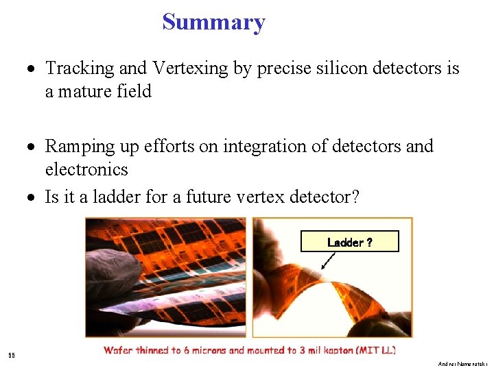
Thin Silicon · After silicon is thinned to 50 micron or less it becomes flexible and eventually transparent 31 Andrei Nomerotski

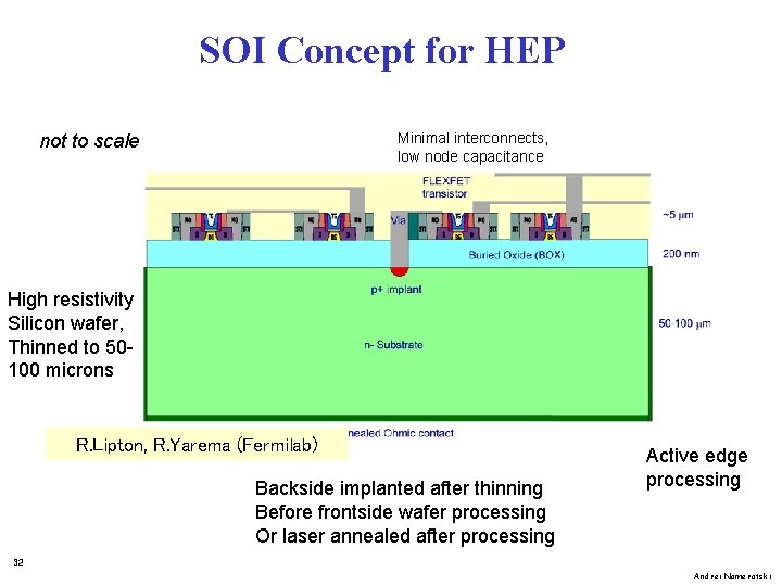
SOI Concept for HEP Minimal interconnects, low node capacitance not to scale High resistivity Silicon wafer, Thinned to 50100 microns R. Lipton, R. Yarema (Fermilab) Backside implanted after thinning Before frontside wafer processing Or laser annealed after processing Active edge processing 32 Andrei Nomerotski

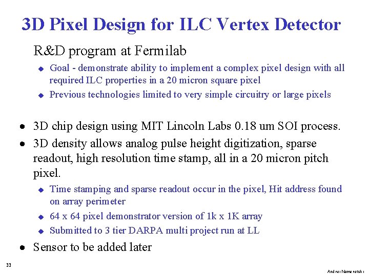
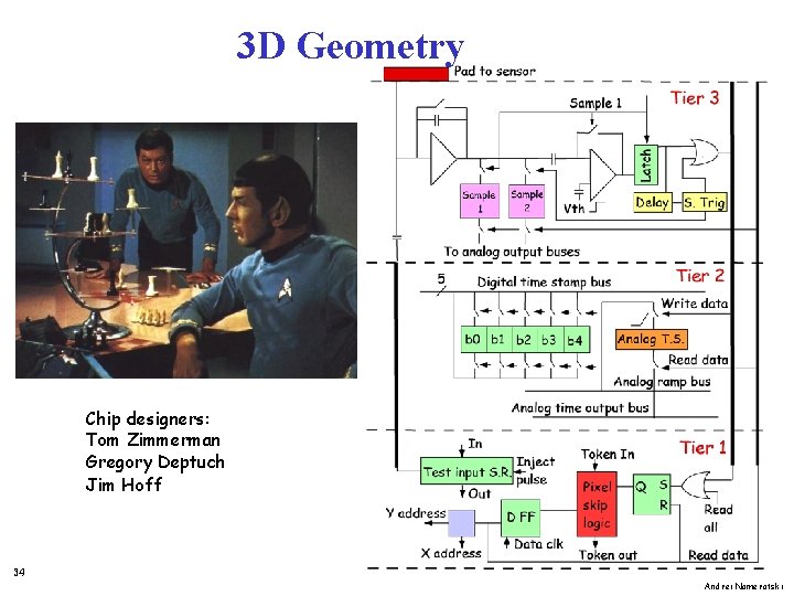
3 D Pixel Design for ILC Vertex Detector R&D program at Fermilab u u Goal - demonstrate ability to implement a complex pixel design with all required ILC properties in a 20 micron square pixel Previous technologies limited to very simple circuitry or large pixels · 3 D chip design using MIT Lincoln Labs 0. 18 um SOI process. · 3 D density allows analog pulse height digitization, sparse readout, high resolution time stamp, all in a 20 micron pitch pixel. u u u Time stamping and sparse readout occur in the pixel, Hit address found on array perimeter 64 x 64 pixel demonstrator version of 1 k x 1 K array Submitted to 3 tier DARPA multi project run at LL · Sensor to be added later 33 Andrei Nomerotski

3 D Geometry Chip designers: Tom Zimmerman Gregory Deptuch Jim Hoff 34 Andrei Nomerotski

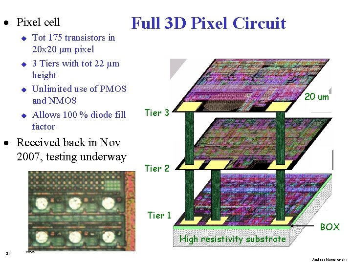
· Pixel cell u u Tot 175 transistors in 20 x 20 µm pixel 3 Tiers with tot 22 µm height Unlimited use of PMOS and NMOS Allows 100 % diode fill factor · Received back in Nov 2007, testing underway Full 3 D Pixel Circuit 20 um Tier 3 Tier 2 Tier 1 High resistivity substrate BOX 35 Andrei Nomerotski

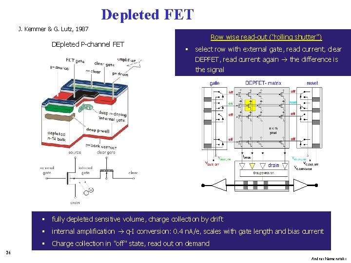
Depleted FET J. Kemmer & G. Lutz, 1987 DEpleted P-channel FET Row wise read-out ("rolling shutter") § select row with external gate, read current, clear DEPFET, read current again the difference is the signal § fully depleted sensitive volume, charge collection by drift § internal amplification q-I conversion: 0. 4 n. A/e, scales with gate length and bias current § Charge collection in "off" state, read out on demand 36 Andrei Nomerotski

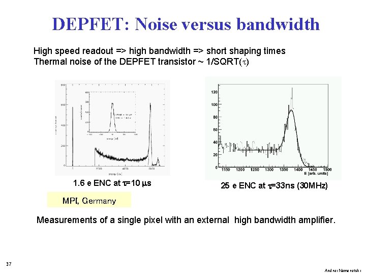
DEPFET: Noise versus bandwidth High speed readout => high bandwidth => short shaping times Thermal noise of the DEPFET transistor ~ 1/SQRT(t) 1. 6 e ENC at t=10 s 25 e ENC at t=33 ns (30 MHz) MPI, Germany Measurements of a single pixel with an external high bandwidth amplifier. 37 Andrei Nomerotski

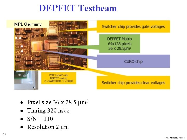
DEPFET Testbeam MPI, Germany · · Pixel size 36 x 28. 5 mm 2 Timing 320 nsec S/N = 110 Resolution 2 mm 38 Andrei Nomerotski

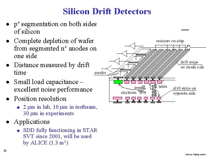
Silicon Drift Detectors · p+ segmentation on both sides of silicon · Complete depletion of wafer from segmented n+ anodes on one side · Distance measured by drift time · Small load capacitance – excellent noise performance · Position resolution u 2 mm in lab, 10 mm in testbeam, 30 mm in experiments · Applications u SDD fully functioning in STAR SVT since 2001, will be used by ALICE (1. 3 m 2) 39 Andrei Nomerotski

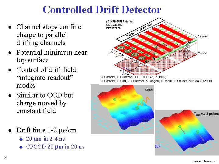
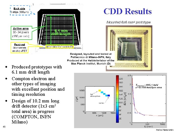
Controlled Drift Detector · Channel stops confine charge to parallel drifting channels · Potential minimum near top surface · Control of drift field: “integrate-readout” modes · Similar to CCD but charge moved by constant field · Drift time 1 -2 ms/cm u u 20 mm in 2 -4 ns CPCCD 20 mm in 20 ns 40 Andrei Nomerotski

CDD Results · Produced prototypes with 6. 1 mm drift length · Compton electron and other types of imaging with excellent position and timing resolution · Design of 10. 2 mm long drift detector (1 x 3 cm 2 total area) in progress (COMPTON, INFN Milano) 41 Andrei Nomerotski

System Issues 42 Andrei Nomerotski

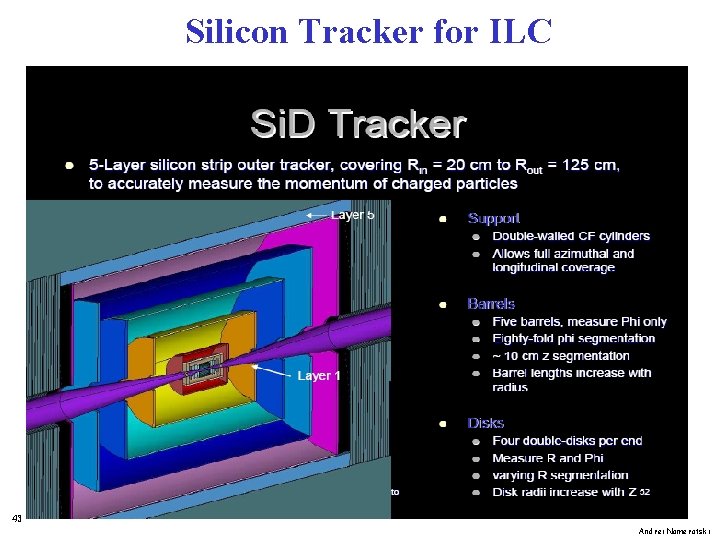
Silicon Tracker for ILC 43 Andrei Nomerotski

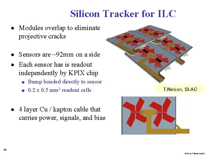
Silicon Tracker for ILC · Modules overlap to eliminate projective cracks · Sensors are ~92 mm on a side · Each sensor has is readout independently by KPIX chip u u Bump bonded directly to sensor 0. 2 x 0. 5 mm 2 readout cells T. Nelson, SLAC · 4 layer Cu / kapton cable that carries power, signals, and bias 44 Andrei Nomerotski

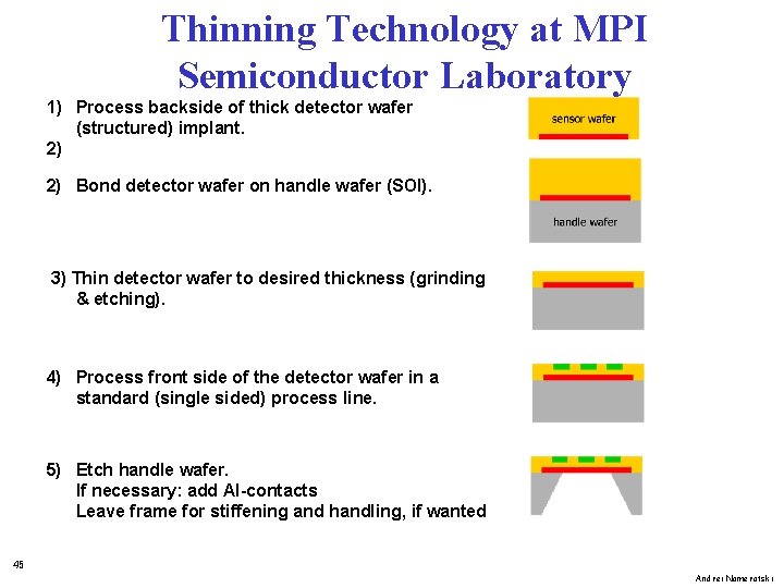
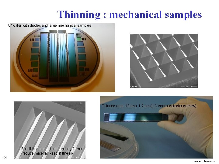
Thinning Technology at MPI Semiconductor Laboratory 1) Process backside of thick detector wafer (structured) implant. 2) 2) Bond detector wafer on handle wafer (SOI). 3) Thin detector wafer to desired thickness (grinding & etching). 4) Process front side of the detector wafer in a standard (single sided) process line. 5) Etch handle wafer. If necessary: add Al-contacts Leave frame for stiffening and handling, if wanted 45 Andrei Nomerotski

Thinning : mechanical samples 6” wafer with diodes and large mechanical samples Thinned area: 10 cm x 1. 2 cm (ILC vertex detector dummy) Possibility to structure handling frame (reduce material, keep stiffness) 46 Andrei Nomerotski

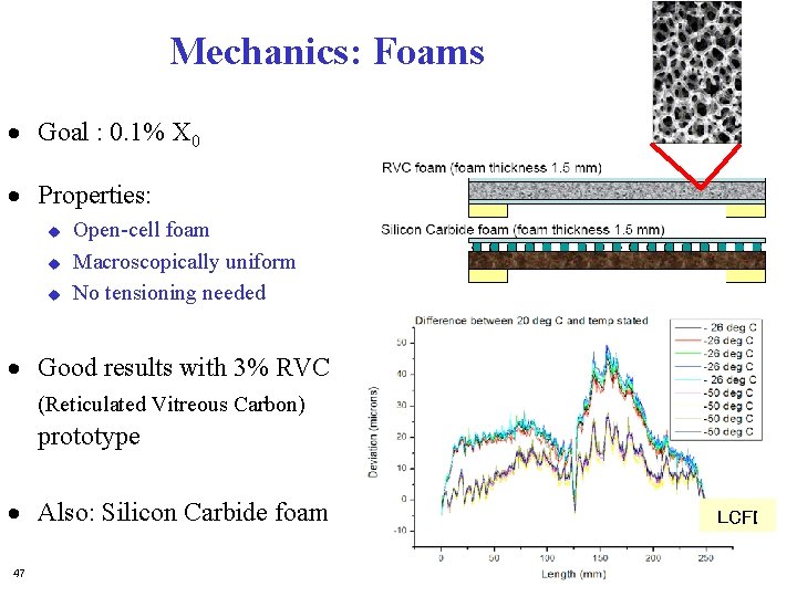
Mechanics: Foams · Goal : 0. 1% X 0 · Properties: u u u Open-cell foam Macroscopically uniform No tensioning needed · Good results with 3% RVC (Reticulated Vitreous Carbon) prototype · Also: Silicon Carbide foam LCFI 47 Andrei Nomerotski

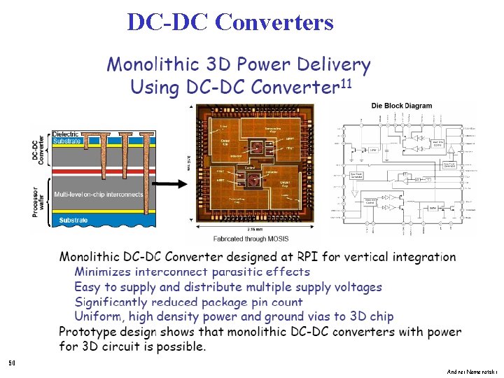
Power Distribution · Power is a crucial issue for the vertex detector u u CP CCD 20 amps x 200 modules = 4000 amps of clock MAPS or SOI 20 -100 W x 100(DF)@1 V = 2000 - 10, 000 amps · Vertex detector technology is sexy - but power engineering is just as important u Serial powering (think Xmas lights) can lower instantaneous current s u u u Understand noise, engineer regulators, understand interconnects Or/and DC-DC converters Lower CCD capacitance Routing in and out s Include something capable of providing 2 -10 k. W in simulation 48 Andrei Nomerotski

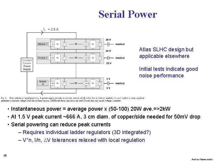
Serial Power Atlas SLHC design but applicable elsewhere Initial tests indicate good noise performance • Instantaneous power = average power x (50 -100) 20 W ave. =>2 k. W • At 1. 5 V peak current ~666 A, 3 cm diam. of copper/side needed for 50 m. V drop • Serial powering can reduce peak currents – Requires individual ladder regulators (3 D integrated? ) – V*n, I/n, V tolerances relaxed with local regulation 49 Andrei Nomerotski

DC-DC Converters 50 Andrei Nomerotski

Applications 51 Andrei Nomerotski

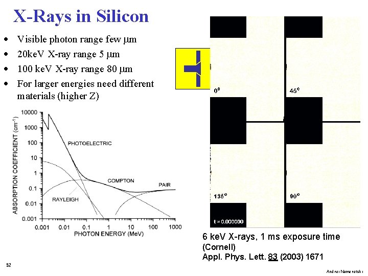
X-Rays in Silicon · · Visible photon range few mm 20 ke. V X-ray range 5 mm 100 ke. V X-ray range 80 mm For larger energies need different materials (higher Z) 6 ke. V X-rays, 1 ms exposure time (Cornell) Appl. Phys. Lett. 83 (2003) 1671 52 Andrei Nomerotski

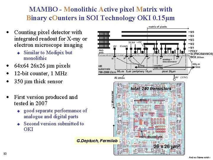
MAMBO - Monolithic Active pixel Matrix with Binary c. Ounters in SOI Technology OKI 0. 15µm · Counting pixel detector with integrated readout for X-ray or electron microscope imaging u Similar to Medipix but monolithic · 64 x 64 26 x 26 mm pixels · 12 -bit counter, 1 MHz · 350 mm thick sensor total: 280 transistors · First version produced and tested in 2007 u u good separate performance of analogue and digital parts Second version submitted to OKI G. Deptuch, Fermilab 26 x 26 m 2 53 Andrei Nomerotski

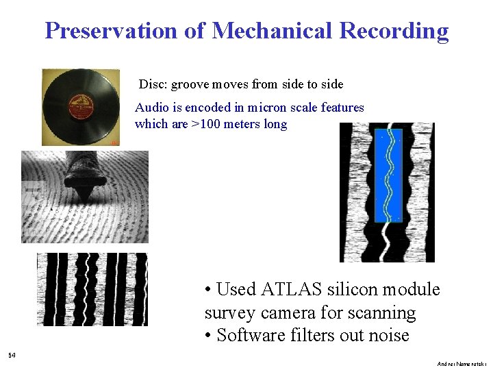
Preservation of Mechanical Recording Disc: groove moves from side to side Audio is encoded in micron scale features which are >100 meters long • Used ATLAS silicon module survey camera for scanning • Software filters out noise 54 Andrei Nomerotski

Summary · Tracking and Vertexing by precise silicon detectors is a mature field · Ramping up efforts on integration of detectors and electronics · Is it a ladder for a future vertex detector? Ladder ? 55 Andrei Nomerotski