Why silicon detectors Main characteristics of silicon detectors

- Slides: 22

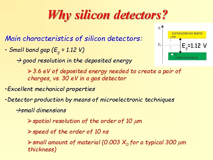
Why silicon detectors? Main characteristics of silicon detectors: • Small band gap (Eg = 1. 12 V) Eg=1. 12 V good resolution in the deposited energy Ø 3. 6 e. V of deposited energy needed to create a pair of charges, vs. 30 e. V in a gas detector • Excellent mechanical properties • Detector production by means of microelectronic techniques small dimensions Øspatial resolution of the order of 10 m Øspeed of the order of 10 ns Øsmall amount of material (0. 003 X 0 for a typical 300 m thickness)

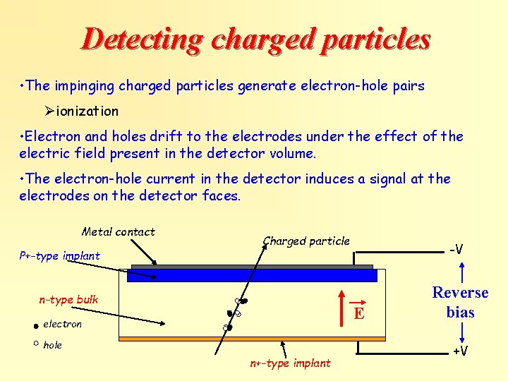
Detecting charged particles • The impinging charged particles generate electron-hole pairs Øionization • Electron and holes drift to the electrodes under the effect of the electric field present in the detector volume. • The electron-hole current in the detector induces a signal at the electrodes on the detector faces. Metal contact P+-type implant Charged particle n-type bulk -V E electron hole n+-type implant Reverse bias +V

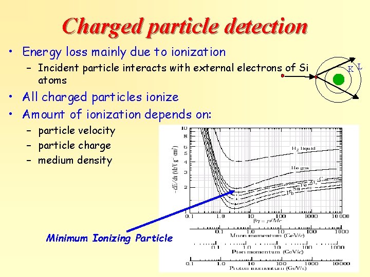
Charged particle detection • Energy loss mainly due to ionization – Incident particle interacts with external electrons of Si atoms • All charged particles ionize • Amount of ionization depends on: – particle velocity – particle charge – medium density Minimum Ionizing Particle K L

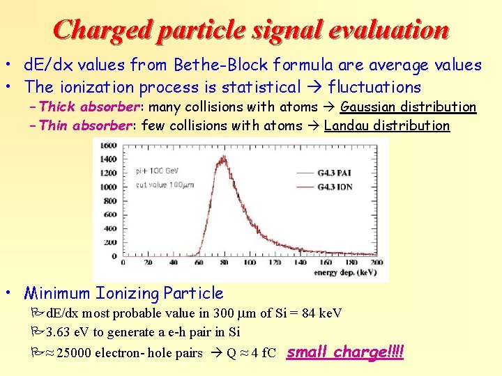
Charged particle signal evaluation • d. E/dx values from Bethe-Block formula are average values • The ionization process is statistical fluctuations – Thick absorber: many collisions with atoms Gaussian distribution – Thin absorber: few collisions with atoms Landau distribution • Minimum Ionizing Particle Pd. E/dx most probable value in 300 mm of Si = 84 ke. V P 3. 63 e. V to generate a e-h pair in Si P≈ 25000 electron- hole pairs Q ≈ 4 f. C small charge!!!!

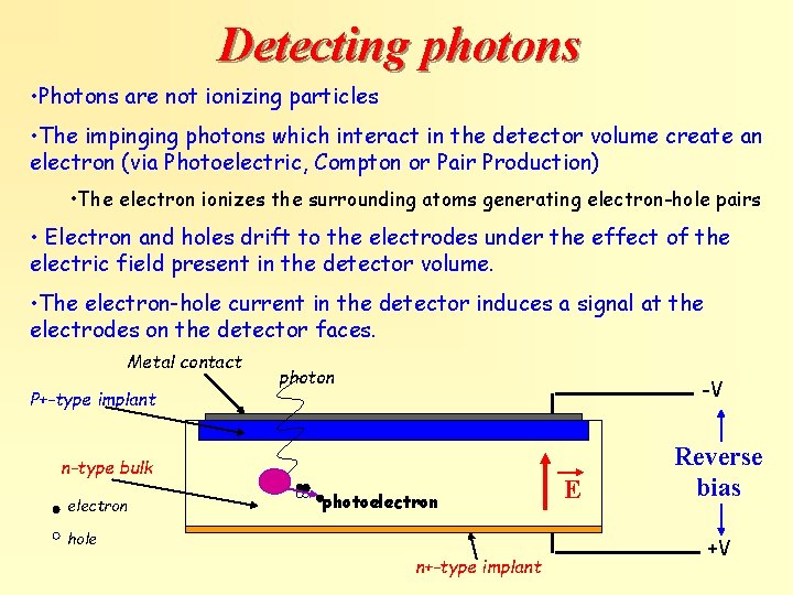
Detecting photons • Photons are not ionizing particles • The impinging photons which interact in the detector volume create an electron (via Photoelectric, Compton or Pair Production) • The electron ionizes the surrounding atoms generating electron-hole pairs • Electron and holes drift to the electrodes under the effect of the electric field present in the detector volume. • The electron-hole current in the detector induces a signal at the electrodes on the detector faces. Metal contact P+-type implant photon -V n-type bulk electron photoelectron hole n+-type implant E Reverse bias +V

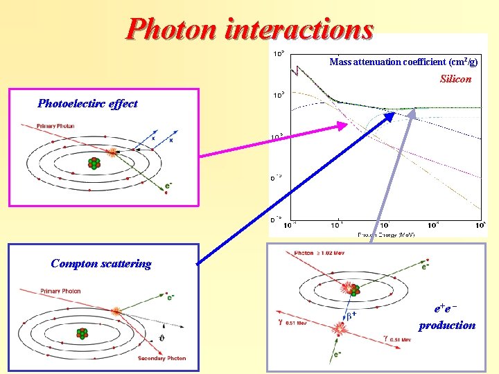
Photon interactions Mass attenuation coefficient (cm 2/g) Silicon Photoelectirc effect Compton scattering _ e+e production

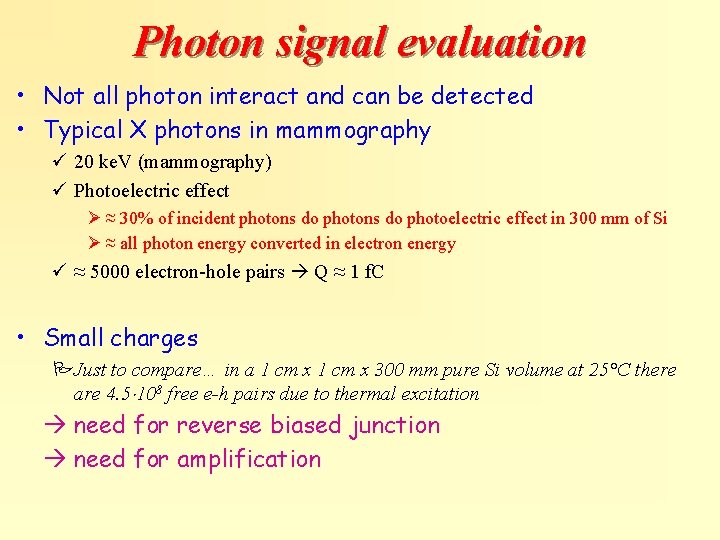
Photon signal evaluation • Not all photon interact and can be detected • Typical X photons in mammography ü 20 ke. V (mammography) ü Photoelectric effect Ø ≈ 30% of incident photons do photoelectric effect in 300 mm of Si Ø ≈ all photon energy converted in electron energy ü ≈ 5000 electron-hole pairs Q ≈ 1 f. C • Small charges PJust to compare… in a 1 cm x 300 mm pure Si volume at 25°C there are 4. 5 108 free e-h pairs due to thermal excitation need for reverse biased junction need for amplification

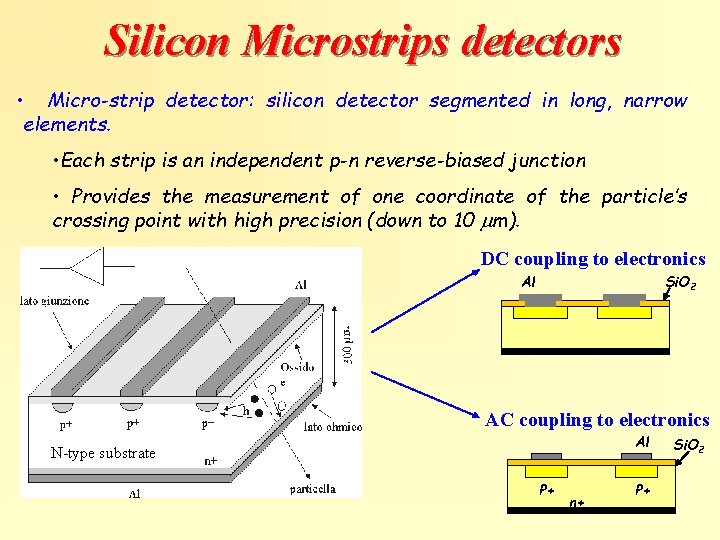
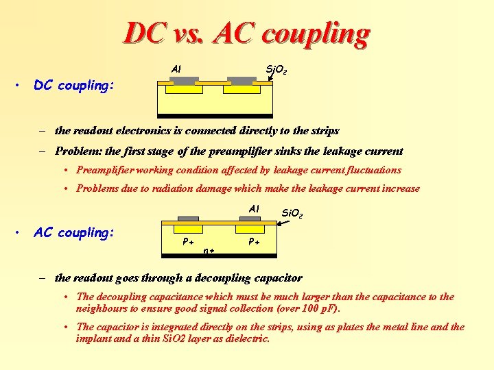
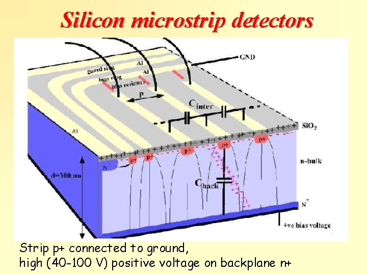
Silicon Microstrips detectors • Micro-strip detector: silicon detector segmented in long, narrow elements. • Each strip is an independent p-n reverse-biased junction • Provides the measurement of one coordinate of the particle’s crossing point with high precision (down to 10 m). DC coupling to electronics Al Si. O 2 AC coupling to electronics Al N-type substrate P+ n+ P+ Si. O 2

DC vs. AC coupling • DC coupling: Al Si. O 2 – the readout electronics is connected directly to the strips – Problem: the first stage of the preamplifier sinks the leakage current • Preamplifier working condition affected by leakage current fluctuations • Problems due to radiation damage which make the leakage current increase Al • AC coupling: P+ n+ Si. O 2 P+ – the readout goes through a decoupling capacitor • The decoupling capacitance which must be much larger than the capacitance to the neighbours to ensure good signal collection (over 100 p. F). • The capacitor is integrated directly on the strips, using as plates the metal line and the implant and a thin Si. O 2 layer as dielectric.

Silicon microstrip detectors Strip p+ connected to ground, high (40 -100 V) positive voltage on backplane n+

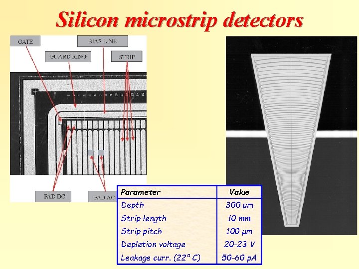
Silicon microstrip detectors Parameter Value Depth 300 μm Strip length 10 mm Strip pitch 100 μm Depletion voltage 20 -23 V Leakage curr. (22º C) 50 -60 p. A

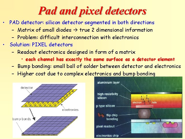
Pad and pixel detectors • PAD detector: silicon detector segmented in both directions – Matrix of small diodes true 2 dimensional information – Problem: difficult interconnection with electronics • Solution: PIXEL detectors – Readout electronics designed in form of a matrix • each channel has exactly the same surface as a detector element – Bump bonding: small ball of solder between detector and electronics – Higher cost due to complex electronics and bump bonding

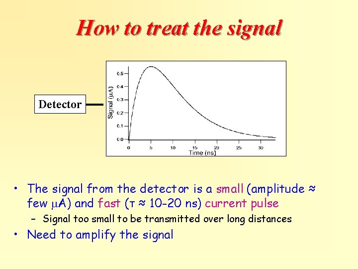
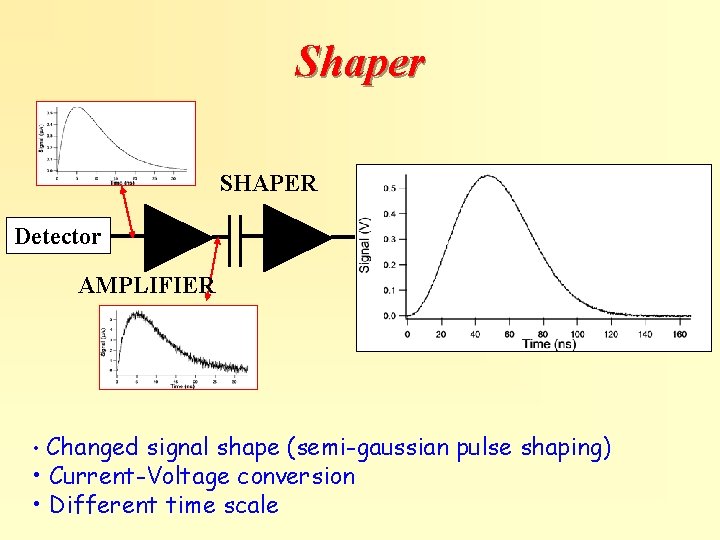
How to treat the signal Detector • The signal from the detector is a small (amplitude ≈ few m. A) and fast (τ ≈ 10 -20 ns) current pulse – Signal too small to be transmitted over long distances • Need to amplify the signal

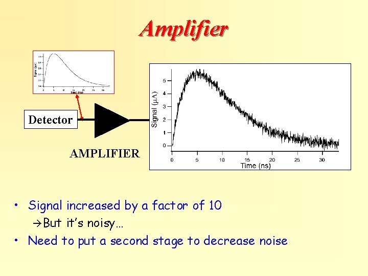
Amplifier Detector AMPLIFIER • Signal increased by a factor of 10 But it’s noisy… • Need to put a second stage to decrease noise

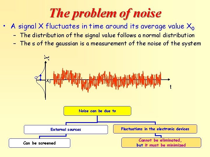
The problem of noise • A signal X fluctuates in time around its average value X 0 X – The distribution of the signal value follows a normal distribution – The s of the gaussian is a measurement of the noise of the system s x 0 t Noise can be due to External sources Can be screened Fluctuations in the electronic devices Cannot be eliminated, but it must be minimized

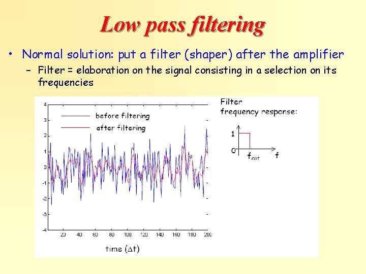
Low pass filtering • Normal solution: put a filter (shaper) after the amplifier – Filter = elaboration on the signal consisting in a selection on its frequencies

Shaper SHAPER Detector AMPLIFIER • Changed signal shape (semi-gaussian pulse shaping) • Current-Voltage conversion • Different time scale

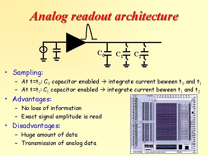
Readout architecture • The signal after the shaper is a continuous function (analog) – Infinite number of “points” – Not good for computer storage and analysis • Digital signals: – Discrete number of signals in time domain (sampling) • Select a finite number of “points” • Store the value of the signals in this discrete set of “points” – Discrete signal amplitude (digitization) • Loss of information • The extent of this loss depends on the number of bits used to represent the amplitude • Technology: – Discrete components vs. integrated (VLSI) circuits

Analog readout architecture C 0 C 1 C 2 • Sampling: – At t=t 0: C 0 capacitor enabled integrate current beween t 0 and t 1 – At t=t 1: C 1 capacitor enabled integrate current beween t 1 and t 2 • Advantages: – No loss of information – Exact signal amplitude is read • Disadvantages: – Huge amount of data – Transmission of analog data

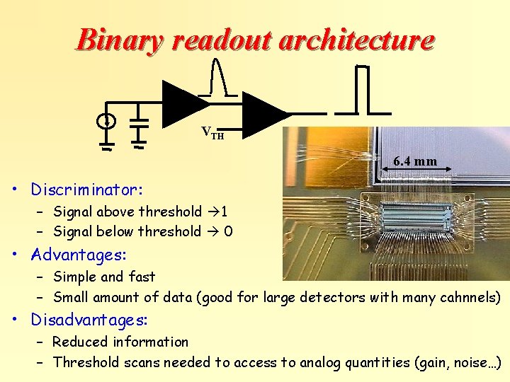
Binary readout architecture VTH 6. 4 mm • Discriminator: – Signal above threshold 1 – Signal below threshold 0 • Advantages: – Simple and fast – Small amount of data (good for large detectors with many cahnnels) • Disadvantages: – Reduced information – Threshold scans needed to access to analog quantities (gain, noise…)

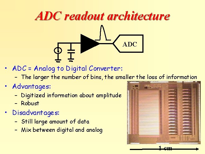
ADC readout architecture ADC • ADC = Analog to Digital Converter: – The larger the number of bins, the smaller the loss of information • Advantages: – Digitized information about amplitude – Robust • Disadvantages: – Still large amount of data – Mix between digital and analog 1 cm

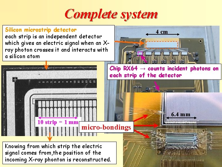
Complete system Silicon microstrip detector each strip is an independent detector which gives an electric signal when an Xray photon crosses it and interacts with a silicon atom 4 cm Chip RX 64 → counts incident photons on each strip of the detector 6. 4 mm 10 strip = 1 mm micro-bondings Knowing from which strip the electric signal comes from, the position of the incoming X-ray phonton is reconstructed.