Position Sensitive Detectors in HEP Silicon Detectors for
- Slides: 31

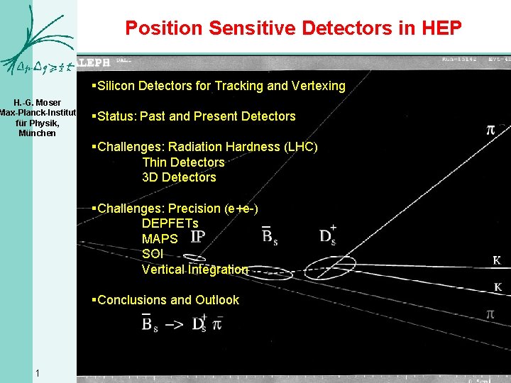
Position Sensitive Detectors in HEP §Silicon Detectors for Tracking and Vertexing H. -G. Moser Max-Planck-Institut für Physik, München §Status: Past and Present Detectors §Challenges: Radiation Hardness (LHC) Thin Detectors 3 D Detectors §Challenges: Precision (e+e-) DEPFETs MAPS SOI Vertical Integration §Conclusions and Outlook 1

Position sensitive detectors From Wikipedia, the free encyclopedia: H. -G. Moser Max-Planck-Institut für Physik, München A Position Sensitive Device and/or Position Sensitive Detector (PSD) is an optical position sensor (OPS), that can measure a position of a light spot in one or two-dimensions on a sensor surface. In particle physics we use this principle to measure - Impact point of ionizing particles (tracker or vertex detector) Or, in astronomy and photon science - Conversion point of a x-ray photon Disclaimer: Most of the talk will be on tracking detectors, ignoring largely x-ray detectors 2 Solid state devices other than silicon are ignored as well

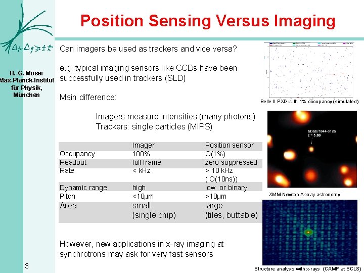
Position Sensing Versus Imaging Can imagers be used as trackers and vice versa? H. -G. Moser Max-Planck-Institut für Physik, München e. g. typical imaging sensors like CCDs have been successfully used in trackers (SLD) Main difference: Belle II PXD with 1% occupancy (simulated) Imagers measure intensities (many photons) Trackers: single particles (MIPS) Occupancy Readout Rate Imager 100% full frame < k. Hz Dynamic range Pitch high <10µm Position sensor O(1%) zero suppressed > 10 k. Hz ( O(10 ns)) low or binary >10µm Area small (single chip) large (tiles, buttable) XMM Newton X-xray astronomy However, new applications in x-ray imaging at synchrotrons may ask for very fast sensors 3 Structure analysis with x-rays (CAMP at SCLS)

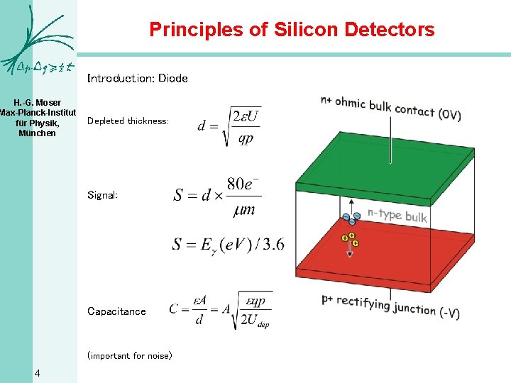
Principles of Silicon Detectors Introduction: Diode H. -G. Moser Max-Planck-Institut für Physik, München Depleted thickness: Signal: Capacitance (important for noise) 4

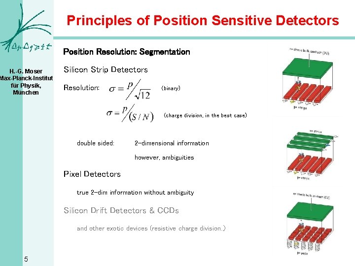
Principles of Position Sensitive Detectors Position Resolution: Segmentation H. -G. Moser Max-Planck-Institut für Physik, München Silicon Strip Detectors Resolution: (binary) (charge division, in the best case) double sided: 2 -dimensional information however, ambiguities Pixel Detectors true 2 -dim information without ambiguity Silicon Drift Detectors & CCDs and other exotic devices (resistive charge division. . ) 5

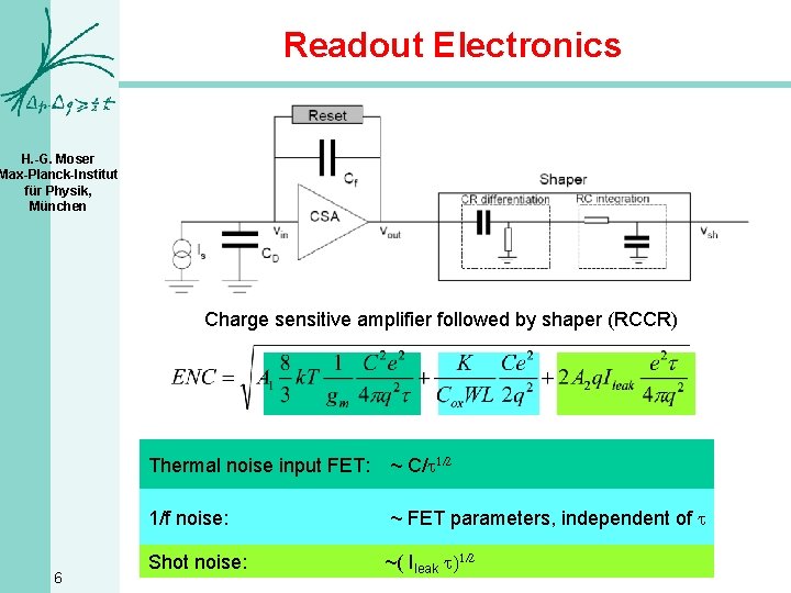
Readout Electronics H. -G. Moser Max-Planck-Institut für Physik, München Charge sensitive amplifier followed by shaper (RCCR) 6 Thermal noise input FET: ~ C/t 1/2 1/f noise: ~ FET parameters, independent of t Shot noise: ~( Ileak t)1/2

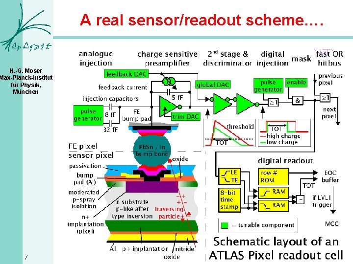
A real sensor/readout scheme…. H. -G. Moser Max-Planck-Institut für Physik, München 7

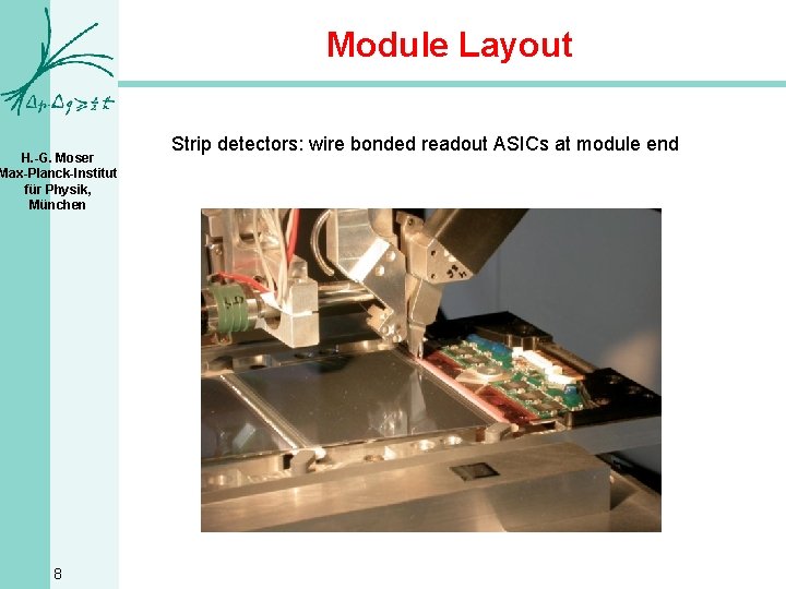
Module Layout H. -G. Moser Max-Planck-Institut für Physik, München 8 Strip detectors: wire bonded readout ASICs at module end

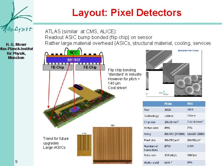
Layout: Pixel Detectors H. -G. Moser Max-Planck-Institut für Physik, München ATLAS (similar at CMS, ALICE): Readout ASIC bump bonded (flip chip) on sensor Rather large material overhead (ASICs, structural material, cooling, services Flip chip bonding ‘standard’ in industry However for pitch > 140 µm Cost driver! Trend for future upgrades Large r. ASICs 9

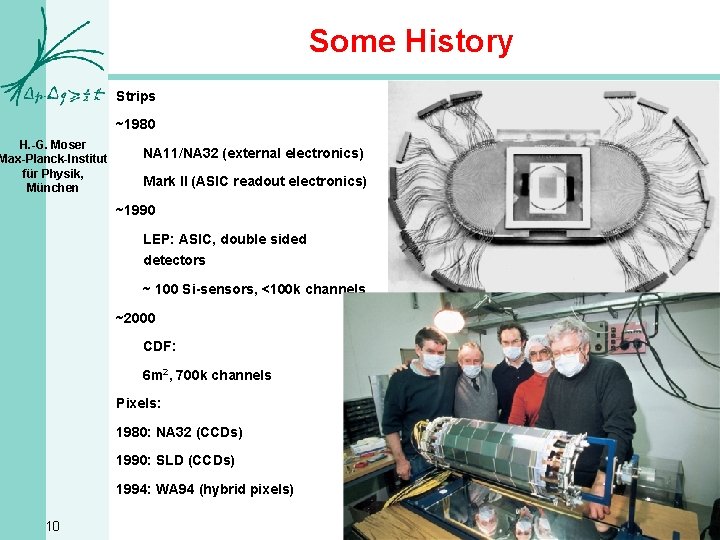
Some History Strips ~1980 H. -G. Moser Max-Planck-Institut für Physik, München NA 11/NA 32 (external electronics) Mark II (ASIC readout electronics) ~1990 LEP: ASIC, double sided detectors ~ 100 Si-sensors, <100 k channels ~2000 CDF: 6 m 2, 700 k channels Pixels: 1980: NA 32 (CCDs) 1990: SLD (CCDs) 1994: WA 94 (hybrid pixels) 10

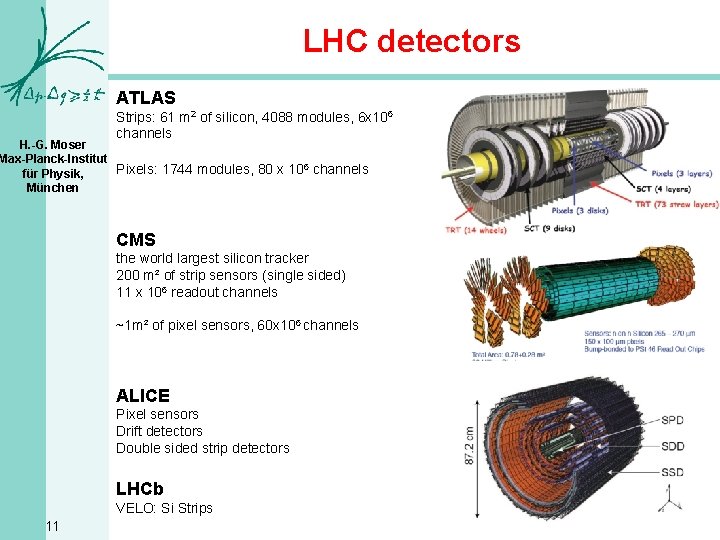
LHC detectors ATLAS Strips: 61 m 2 of silicon, 4088 modules, 6 x 10⁶ channels H. -G. Moser Max-Planck-Institut Pixels: 1744 modules, 80 x 106 channels für Physik, München CMS the world largest silicon tracker 200 m² of strip sensors (single sided) 11 x 106 readout channels ~1 m² of pixel sensors, 60 x 106 channels ALICE Pixel sensors Drift detectors Double sided strip detectors LHCb VELO: Si Strips 11

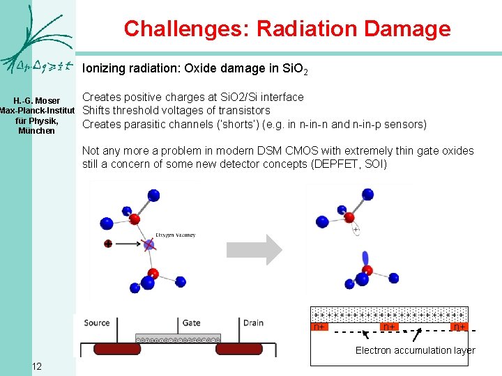
Challenges: Radiation Damage Ionizing radiation: Oxide damage in Si. O 2 H. -G. Moser Max-Planck-Institut für Physik, München Creates positive charges at Si. O 2/Si interface Shifts threshold voltages of transistors Creates parasitic channels (‘shorts’) (e. g. in n-in-n and n-in-p sensors) Not any more a problem in modern DSM CMOS with extremely thin gate oxides still a concern of some new detector concepts (DEPFET, SOI) ++++++++++++ n+ --- - - -n+ - - - - - n+ Electron accumulation layer 12

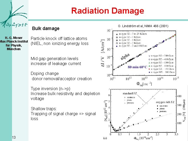
Radiation Damage Bulk damage H. -G. Moser Max-Planck-Institut für Physik, München Particle knock off lattice atoms (NIEL, non ionizing energy loss Mid gap generation levels increase of leakage current Doping change donor removal/acceptor creation Type inversion (n->p) Increase bulk resistivity and depletion voltage Shallow traps: Trapping of signal charge => signal loss 13 G. Lindström et al, NIMA 466 (2001)

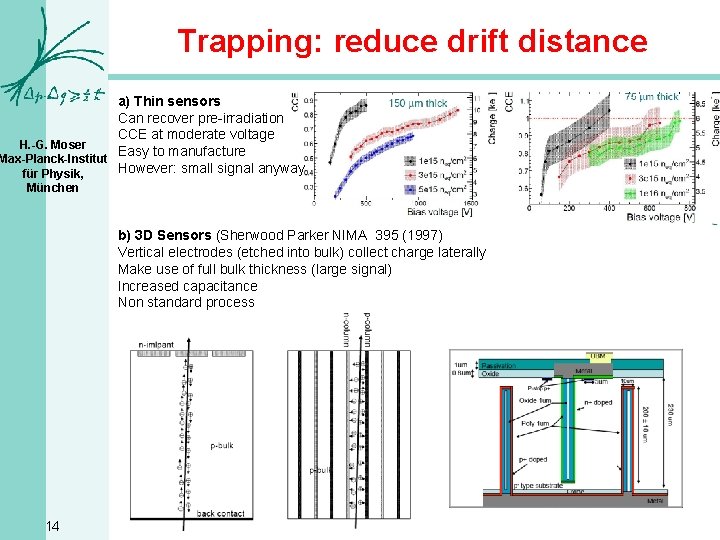
Trapping: reduce drift distance a) Thin sensors Can recover pre-irradiation CCE at moderate voltage H. -G. Moser Easy to manufacture Max-Planck-Institut However: small signal anyway für Physik, München b) 3 D Sensors (Sherwood Parker NIMA 395 (1997) Vertical electrodes (etched into bulk) collect charge laterally Make use of full bulk thickness (large signal) Increased capacitance Non standard process 14

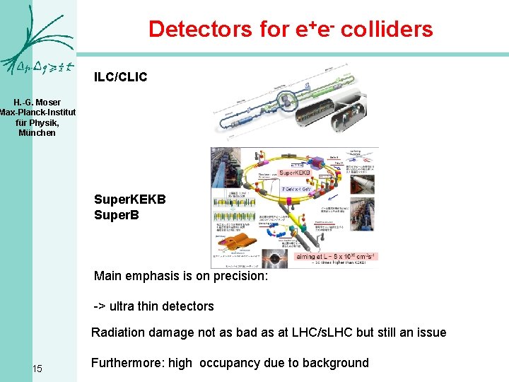
Detectors for e+e- colliders ILC/CLIC H. -G. Moser Max-Planck-Institut für Physik, München Super. KEKB Super. B Main emphasis is on precision: -> ultra thin detectors Radiation damage not as bad as at LHC/s. LHC but still an issue 15 Furthermore: high occupancy due to background

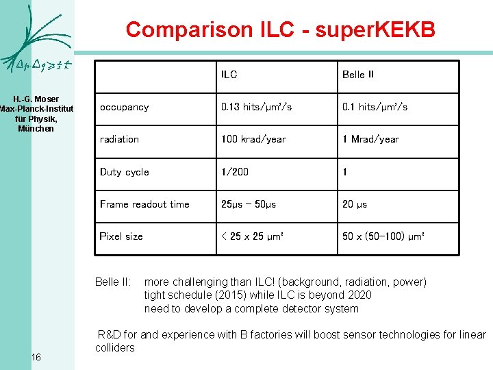
Comparison ILC - super. KEKB H. -G. Moser Max-Planck-Institut für Physik, München ILC Belle II occupancy 0. 13 hits/µm²/s 0. 1 hits/µm²/s radiation 100 krad/year 1 Mrad/year Duty cycle 1/200 1 Frame readout time 25µs – 50µs 20 µs Pixel size < 25 x 25 µm² 50 x (50 -100) µm² Belle II: 16 more challenging than ILC! (background, radiation, power) tight schedule (2015) while ILC is beyond 2020 need to develop a complete detector system R&D for and experience with B factories will boost sensor technologies for linear colliders

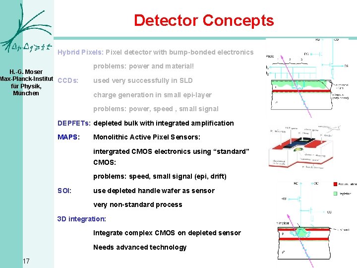
Detector Concepts Hybrid Pixels: Pixel detector with bump-bonded electronics H. -G. Moser Max-Planck-Institut CCDs: für Physik, München problems: power and material! used very successfully in SLD charge generation in small epi-layer problems: power, speed , small signal DEPFETs: depleted bulk with integrated amplification MAPS: Monolithic Active Pixel Sensors: intergrated CMOS electronics using “standard” CMOS: problems: speed, small signal (epi, drift) SOI: use depleted handle wafer as sensor very non-standard process 3 D integration: Integrate complex CMOS on depleted sensor Needs advanced technology 17 CCD

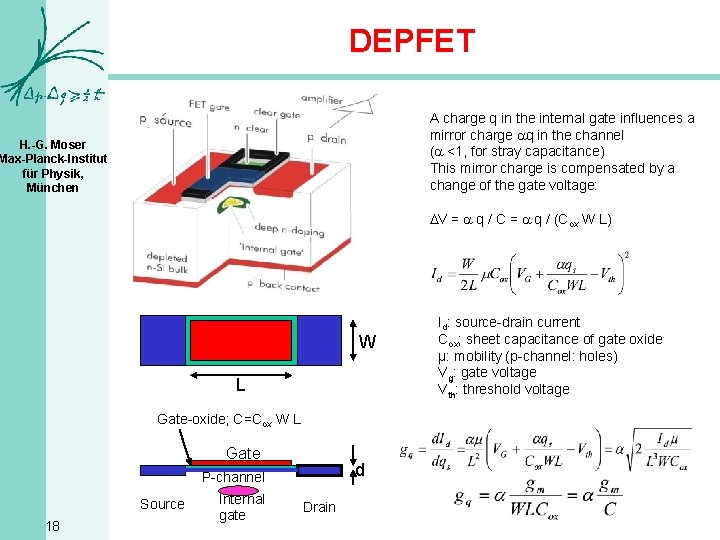
DEPFET A charge q in the internal gate influences a mirror charge aq in the channel (a <1, for stray capacitance) This mirror charge is compensated by a change of the gate voltage: H. -G. Moser Max-Planck-Institut für Physik, München DV = a q / C = a q / (Cox W L) W L Gate-oxide; C=Cox W L Gate d P-channel Source 18 Internal gate Drain Id: source-drain current Cox; sheet capacitance of gate oxide µ: mobility (p-channel: holes) Vg: gate voltage Vth: threshold voltage

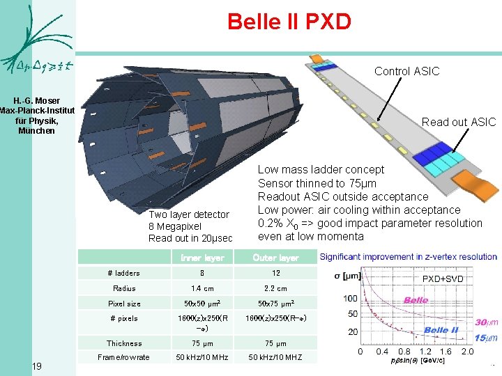
Belle II PXD Control ASIC H. -G. Moser Max-Planck-Institut für Physik, München Read out ASIC Two layer detector 8 Megapixel Read out in 20µsec 19 Low mass ladder concept Sensor thinned to 75µm Readout ASIC outside acceptance Low power: air cooling within acceptance 0. 2% X 0 => good impact parameter resolution even at low momenta Inner layer Outer layer # ladders 8 12 Radius 1. 4 cm 2. 2 cm Pixel size 50 x 50 µm 2 50 x 75 µm 2 # pixels 1600(z)x 250(R -ɸ) 1600(z)x 250(R-ɸ) Thickness 75 µm Frame/row rate 50 k. Hz/10 MHz 50 k. Hz/10 MHZ

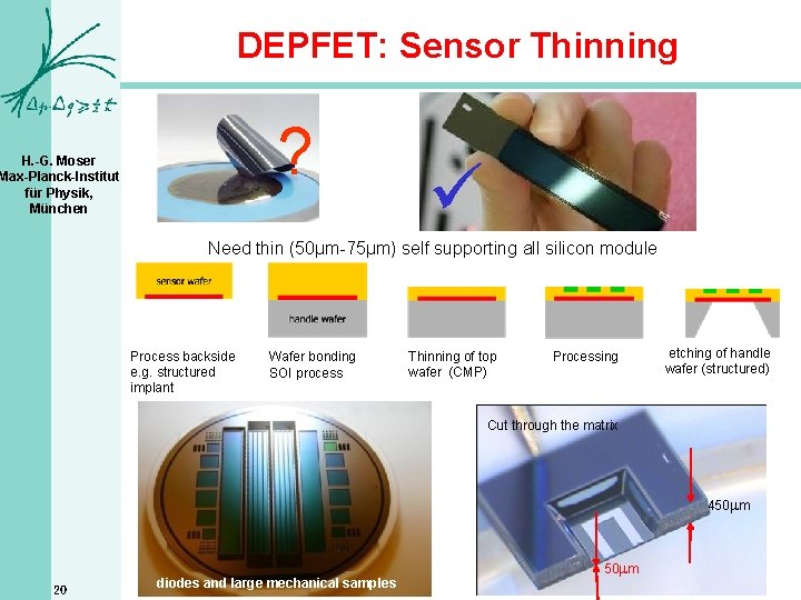
DEPFET: Sensor Thinning ? H. -G. Moser Max-Planck-Institut für Physik, München ü Need thin (50µm-75µm) self supporting all silicon module Process backside e. g. structured implant Wafer bonding SOI process Thinning of top wafer (CMP) Processing etching of handle wafer (structured) Cut through the matrix 450 mm 20 diodes large mechanical samples diodes andand large mecanical samples 50 mm Belle II module

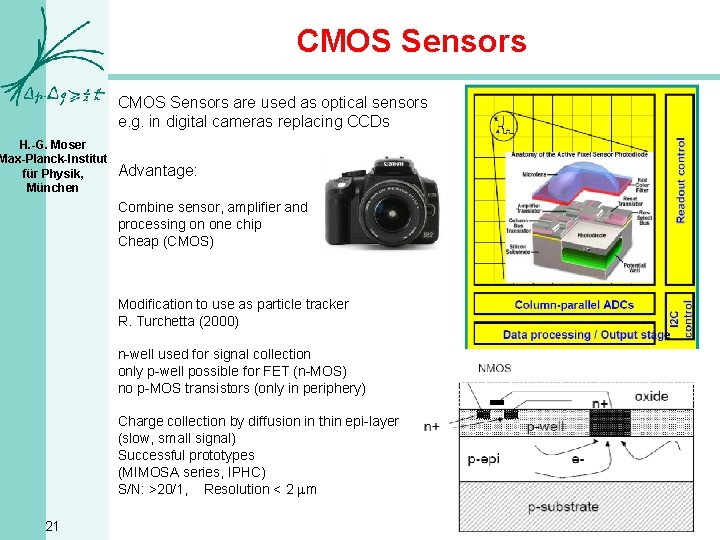
CMOS Sensors are used as optical sensors e. g. in digital cameras replacing CCDs H. -G. Moser Max-Planck-Institut für Physik, München Advantage: Combine sensor, amplifier and processing on one chip Cheap (CMOS) Modification to use as particle tracker R. Turchetta (2000) n-well used for signal collection only p-well possible for FET (n-MOS) no p-MOS transistors (only in periphery) Charge collection by diffusion in thin epi-layer (slow, small signal) Successful prototypes (MIMOSA series, IPHC) S/N: >20/1, Resolution < 2 mm 21

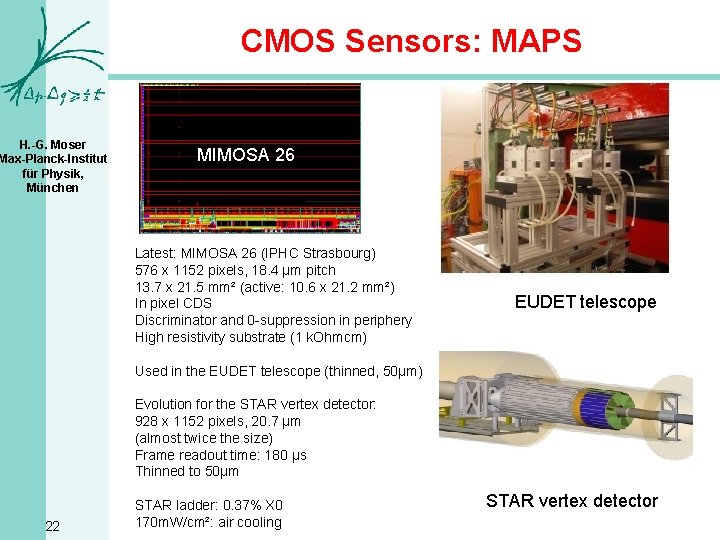
CMOS Sensors: MAPS H. -G. Moser Max-Planck-Institut für Physik, München MIMOSA 26 Latest: MIMOSA 26 (IPHC Strasbourg) 576 x 1152 pixels, 18. 4 µm pitch 13. 7 x 21. 5 mm² (active: 10. 6 x 21. 2 mm²) In pixel CDS Discriminator and 0 -suppression in periphery High resistivity substrate (1 k. Ohmcm) EUDET telescope Used in the EUDET telescope (thinned, 50µm) Evolution for the STAR vertex detector: 928 x 1152 pixels, 20. 7 µm (almost twice the size) Frame readout time: 180 µs Thinned to 50µm 22 STAR ladder: 0. 37% X 0 170 m. W/cm²: air cooling STAR vertex detector

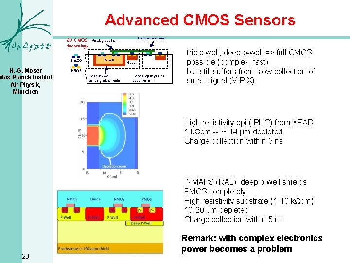
Advanced CMOS Sensors Digital section 2 D CMOS Analog section technology NMOS H. -G. Moser Max-Planck-Institut für Physik, München PMOS P-well Deep N-well sensing electrode N-well P-type epilayer or substrate triple well, deep p-well => full CMOS possible (complex, fast) but still suffers from slow collection of small signal (VIPIX) High resistivity epi (IPHC) from XFAB 1 k. Wcm -> ~ 14 µm depleted Charge collection within 5 ns INMAPS (RAL): deep p-well shields PMOS completely High resistivity substrate (1 -10 k. Wcm) 10 -20 µm depleted Charge collection within 5 ns 23 Remark: with complex electronics power becomes a problem

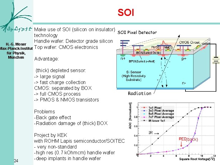
SOI Make use of SOI (silicon on insulator) technology Handle wafer: Detector grade silicon H. -G. Moser Max-Planck-Institut Top wafer: CMOS electronics für Physik, München Advantage: (thick) depleted sensor: -> large signal -> fast charge collection CMOS: separated by BOX -> full CMOS process -> PMOS & NMOS transistors Problems -Back gate effect -Radiation damage of (thick) BOX 24 Project by KEK with ROHM Lapis semiconductor/SOITEC - very non-standard -high res (0. 7 k. Ohmcm) handle wafer -deep implants in handle wafer (back)

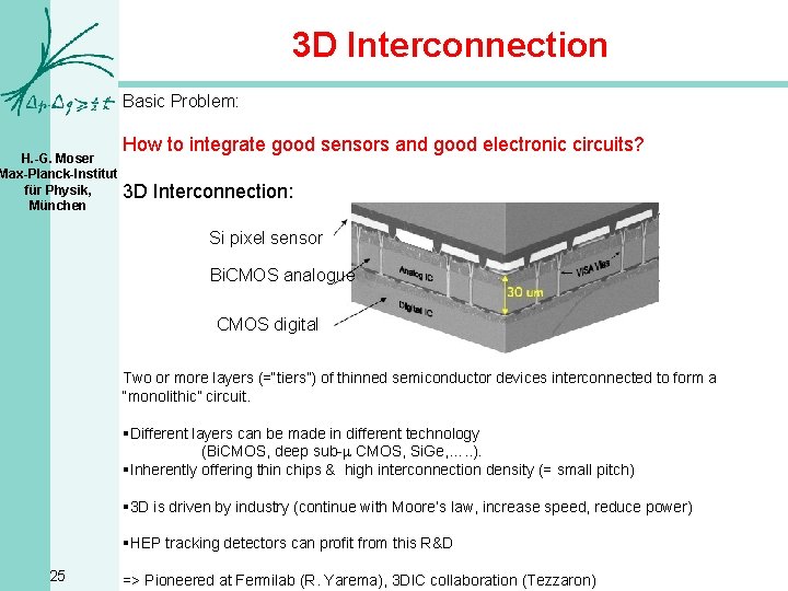
3 D Interconnection Basic Problem: H. -G. Moser Max-Planck-Institut für Physik, München How to integrate good sensors and good electronic circuits? 3 D Interconnection: Si pixel sensor Bi. CMOS analogue CMOS digital Two or more layers (=“tiers”) of thinned semiconductor devices interconnected to form a “monolithic” circuit. §Different layers can be made in different technology (Bi. CMOS, deep sub-m CMOS, Si. Ge, …. . ). §Inherently offering thin chips & high interconnection density (= small pitch) § 3 D is driven by industry (continue with Moore’s law, increase speed, reduce power) §HEP tracking detectors can profit from this R&D 25 => Pioneered at Fermilab (R. Yarema), 3 DIC collaboration (Tezzaron)

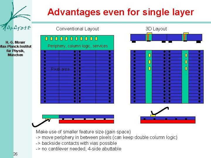
Advantages even for single layer Conventional Layout H. -G. Moser Max-Planck-Institut für Physik, München 3 D Layout Periphery, column logic, services Pixel area Make use of smaller feature size (gain space) -> move periphery in between pixels (can keep double column logic) -> backside contacts with vias possible -> no cantilever needed, 4 -side abuttable 26

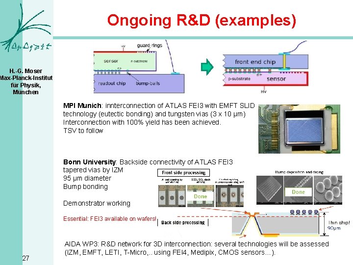
Ongoing R&D (examples) H. -G. Moser Max-Planck-Institut für Physik, München MPI Munich: innterconnection of ATLAS FEI 3 with EMFT SLID technology (eutectic bonding) and tungsten vias (3 x 10 µm) Interconnection with 100% yield has been achieved. TSV to follow Bonn University: Backside connectivity of ATLAS FEI 3 tapered vias by IZM 95 µm diameter Bump bonding Demonstrator working Essential: FEI 3 available on wafers! 27 AIDA WP 3: R&D network for 3 D interconnection: several technologies will be assessed (IZM, EMFT, LETI, T-Micro, . . using FEI 4, Medipix, CMOS sensors…).

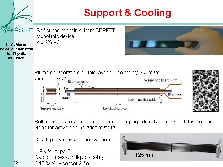
Support & Cooling H. -G. Moser Max-Planck-Institut für Physik, München Self supported thin silicon: DEPFET: Monolithic device < 0. 2% X 0 Plume collaboration: double layer supported by Si. C foam Aim for 0. 3% X 0 Both concepts rely on air cooling, excluding high density sensors with fast readout Need for active cooling adds material! Develop low mass support & cooling: 28 INFN for super. B Carbon tubes with liquid cooling 0. 15 % X 0 + sensor & flex 125 mm

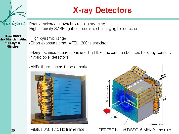
X-ray Detectors Photon science at synchrotrons is booming! High intensity SASE light sources are challenging for detectors H. -G. Moser Max-Planck-Institut für Physik, München -High dynamic range -Short exposure time (XFEL: 200 ns spacing) -Many techniques and ideas used in HEP trackers can be used for x-ray sensors (hybrid pixel detectors) -AND: there seems to be a market! 29 Pilatus 6 M, 12. 5 Hz frame rate DEPFET based DSSC: 5 MHz frame rate

Summary Position sensitive silicon detectors have reached maturity and are an integral part of modern particle physics detectors H. -G. Moser Max-Planck-Institut für Physik, München LHC: large areas of silicon (up to 200 m 2) radiation hard up to 1014 n/cm 2 (strips) 1015 n/cm 2 (pixel) Future need to improve by a factor of 10 ! Performance limited by trapping Promising concepts for >1016 n/cm² B-factories, linear collider: low mass, high resolution, high rate Integration of electronics and sensors a) Monolithic detectors b) 3 D integration 30 key for R&D: find industrial partner who is willing to adapt his process to our needs!

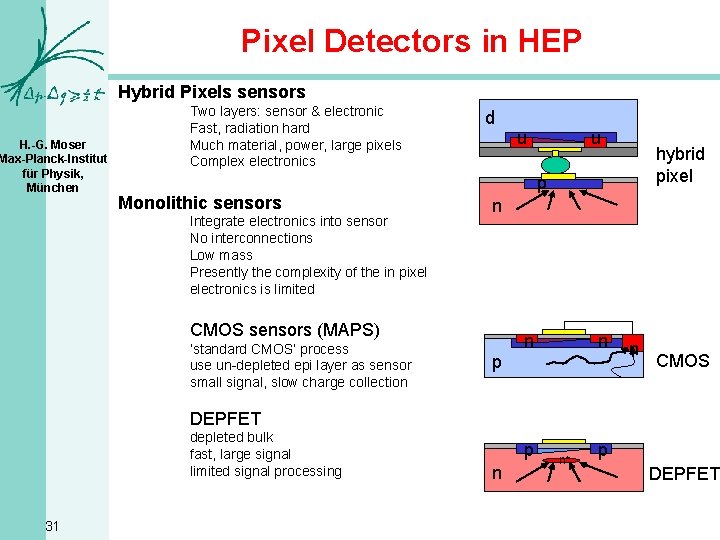
Pixel Detectors in HEP Hybrid Pixels sensors n Integrate electronics into sensor No interconnections Low mass Presently the complexity of the in pixel electronics is limited hybrid pixel ALEPH 1994 p n CMOS sensors (MAPS) ‘standard CMOS’ process use un-depleted epi layer as sensor small signal, slow charge collection n Monolithic sensors p H. -G. Moser Max-Planck-Institut für Physik, München Two layers: sensor & electronic Fast, radiation hard Much material, power, large pixels Complex electronics n n p n CMOS DEPFET depleted bulk fast, large signal limited signal processing 31 p n n+ p DEPFET