Secrets of the DCM Part 2 Steven Knapp





- Slides: 51
Secrets of the DCM: Part 2 Steven Knapp General Products Division (steve. knapp@xilinx. com) NOTICE: This is an early draft of this presentation. Please visit the Xilinx Sales Partner Web (SPW) for the latest version. http: //www. partner. xilinx. com/common/spartan 3/fae © 2004 by Xilinx, Inc. All rights reserved. (v 1. 2, 11 -OCT-2004)
Continuing On … • This is a continuation of Secrets of the DCM: Part 1 that covered the following topics … – Overview of the DCM and its applications – Basic Delay Locked-Loop (DLL) operation – Clock Wizard – Clock Jitter Secrets of the DCM (Part I) 2
Workshop Objectives By the end of this class, you will … • Understand how the DCM can phase shift • • clocks Understand how to generate other clock frequencies Learn how to build high-speed data interfaces Overcome various DCM limitations Legitimately say “DCMs Don’t Confuse Me” Secrets of the DCM (Part I) 3
Lesson Four Phase Shifting
Delay Taps CLKFB Input Stage CLKIN Delay-Locked Loop (DLL) Output Stage DCM Block Diagram DCM CLK 0 CLK 90 CLK 180 CLK 270 CLK 2 X 180 CLKDV Digital CLKFX Frequency CLKFX 180 Synthesizer PSEN PSINCDEC PSCLK RST Secrets of the DCM (Part I) 5 Phase Shifter (PS) Status Logic PSDONE STATUS[7: 0] LOCKED
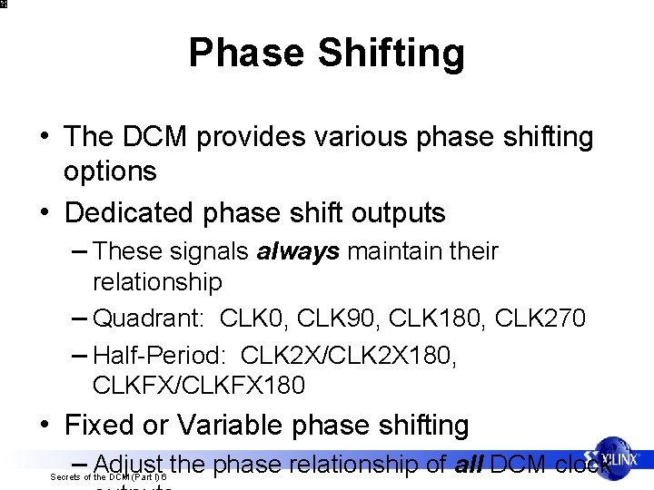
Phase Shifting • The DCM provides various phase shifting options • Dedicated phase shift outputs – These signals always maintain their relationship – Quadrant: CLK 0, CLK 90, CLK 180, CLK 270 – Half-Period: CLK 2 X/CLK 2 X 180, CLKFX/CLKFX 180 • Fixed or Variable phase shifting – Adjust the phase relationship of all DCM clock Secrets of the DCM (Part I) 6
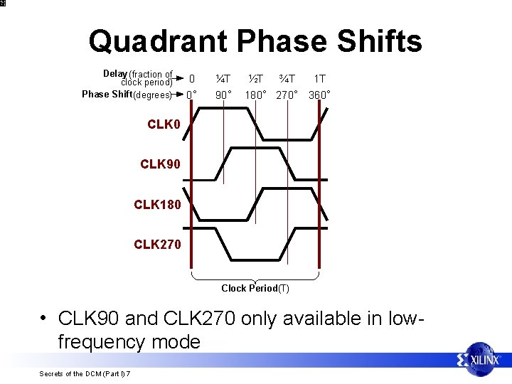
Quadrant Phase Shifts Delay (fraction of clock period) Phase Shift (degrees) 0 ¼T 0° 90° ½T ¾T 1 T 180° 270° 360° CLK 0 CLK 90 CLK 180 CLK 270 Clock Period (T) • CLK 90 and CLK 270 only available in lowfrequency mode Secrets of the DCM (Part I) 7
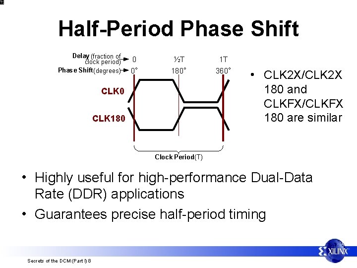
Half-Period Phase Shift Delay (fraction of clock period) Phase Shift (degrees) 0 ½T 1 T 0° 180° 360° • CLK 2 X/CLK 2 X 180 and CLKFX/CLKFX 180 are similar CLK 0 CLK 180 Clock Period (T) • Highly useful for high-performance Dual-Data Rate (DDR) applications • Guarantees precise half-period timing Secrets of the DCM (Part I) 8
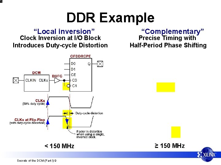
DDR Example “Local inversion” “Complementary” Clock Inversion at I/O Block Introduces Duty-cycle Distortion Precise Timing with Half-Period Phase Shifting < 150 MHz ≥ 150 MHz Secrets of the DCM (Part I) 9
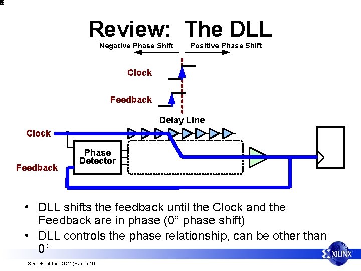
Review: The DLL Negative Phase Shift Positive Phase Shift Clock Feedback Delay Line Clock Feedback Phase Detector • DLL shifts the feedback until the Clock and the Feedback are in phase (0° phase shift) • DLL controls the phase relationship, can be other than 0° Secrets of the DCM (Part I) 10
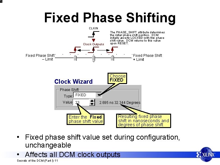
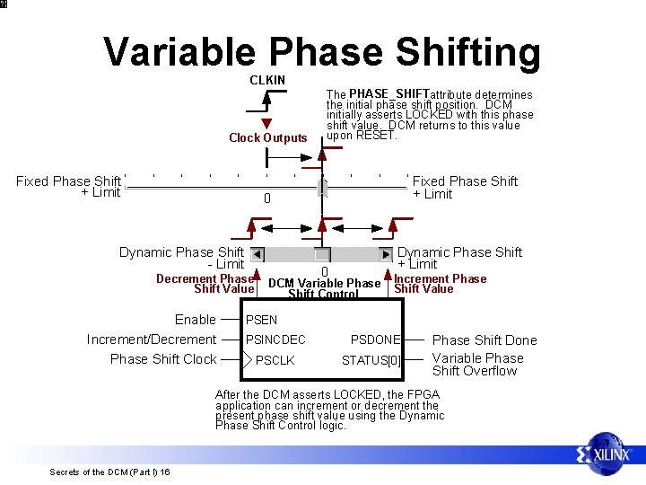
Fixed Phase Shifting CLKIN Clock Outputs Fixed Phase Shift – Limit The PHASE_SHIFT attribute determines the initial phase shift position. DCM initially asserts LOCKED with this phase shift value. DCM returns to this value upon RESET. Fixed Phase Shift + Limit 0 Choose FIXED Clock Wizard Phase Shift FIXED Type: NONE Value: 23 2. 695 ns 32. 344 Degrees Enter the Fixed phase shift value Resulting fixed phase shift in nanoseconds and degrees of phase shift • Fixed phase shift value set during configuration, unchangeable • Affects all DCM clock outputs Secrets of the DCM (Part I) 11
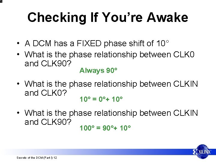
Checking If You’re Awake • A DCM has a FIXED phase shift of 10° • What is the phase relationship between CLK 0 and CLK 90? Always 90° • What is the phase relationship between CLKIN and CLK 0? 10° = 0°+ 10° • What is the phase relationship between CLKIN and CLK 90? Secrets of the DCM (Part I) 12 100° = 90°+ 10°
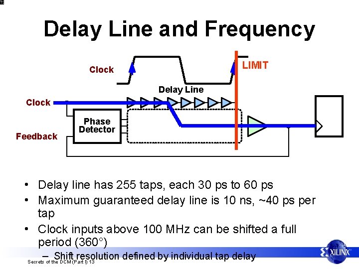
Delay Line and Frequency LIMIT Clock Delay Line Clock Feedback Phase Detector • Delay line has 255 taps, each 30 ps to 60 ps • Maximum guaranteed delay line is 10 ns, ~40 ps per tap • Clock inputs above 100 MHz can be shifted a full period (360°) – Shift resolution defined by individual tap delay Secrets of the DCM (Part I) 13
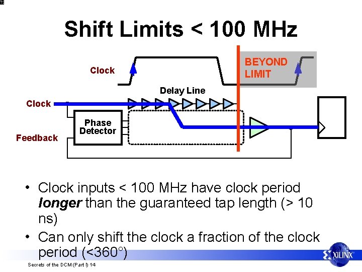
Shift Limits < 100 MHz BEYOND LIMIT Clock Delay Line Clock Feedback Phase Detector • Clock inputs < 100 MHz have clock period longer than the guaranteed tap length (> 10 ns) • Can only shift the clock a fraction of the clock period (<360°) Secrets of the DCM (Part I) 14
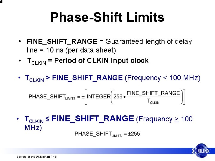
Phase-Shift Limits • FINE_SHIFT_RANGE = Guaranteed length of delay line = 10 ns (per data sheet) • TCLKIN = Period of CLKIN input clock • TCLKIN > FINE_SHIFT_RANGE (Frequency < 100 MHz) • TCLKIN ≤ FINE_SHIFT_RANGE (Frequency > 100 MHz) Secrets of the DCM (Part I) 15
Variable Phase Shifting CLKIN Clock Outputs Fixed Phase Shift + Limit The PHASE_SHIFTattribute determines the initial phase shift position. DCM initially asserts LOCKED with this phase shift value. DCM returns to this value upon RESET. Fixed Phase Shift + Limit 0 Dynamic Phase Shift - Limit Decrement Phase Shift Value Enable Increment/Decrement Phase Shift Clock 0 Dynamic Phase Shift + Limit DCM Variable Phase Shift Control Increment Phase Shift Value PSEN PSINCDEC PSCLK PSDONE STATUS[0] Phase Shift Done Variable Phase Shift Overflow After the DCM asserts LOCKED, the FPGA application can increment or decrement the present phase shift value using the Dynamic Phase Shift Control logic. Secrets of the DCM (Part I) 16
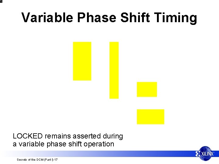
Variable Phase Shift Timing LOCKED remains asserted during a variable phase shift operation Secrets of the DCM (Part I) 17
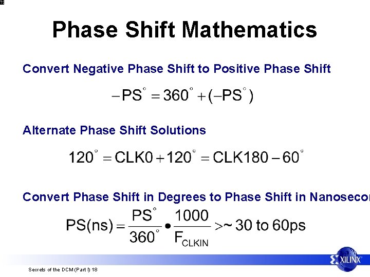
Phase Shift Mathematics Convert Negative Phase Shift to Positive Phase Shift Alternate Phase Shift Solutions Convert Phase Shift in Degrees to Phase Shift in Nanosecon Secrets of the DCM (Part I) 18
Lesson Five Clock Synthesis
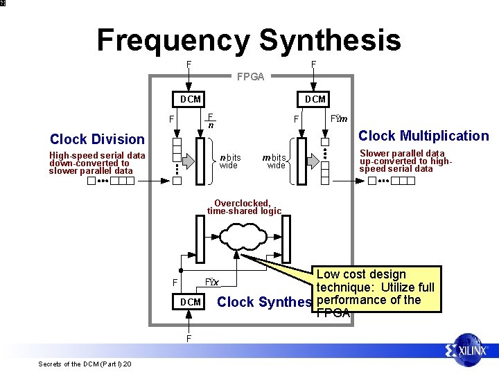
Frequency Synthesis F F FPGA DCM F n F F FŸm Clock Multiplication Clock Division High-speed serial data down-converted to slower parallel data n-bits wide m-bits wide Slower parallel data up-converted to highspeed serial data Overclocked, time-shared logic DCM F Secrets of the DCM (Part I) 20 Low cost design technique: Utilize full performance of the Clock Synthesis FPGA FŸx F
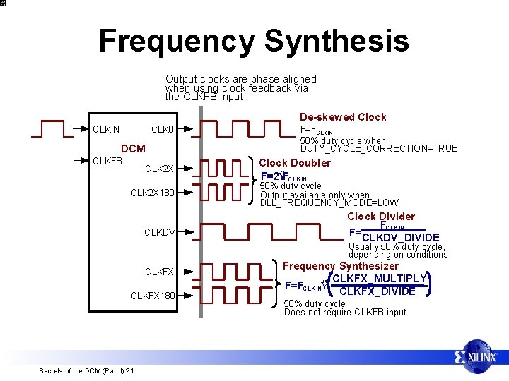
Frequency Synthesis Output clocks are phase aligned when using clock feedback via the CLKFB input. De-skewed Clock CLKIN CLK 0 DCM CLKFB CLK 2 X 180 CLKDV F=FCLKIN 50% duty cycle when DUTY_CYCLE_CORRECTION=TRUE Clock Doubler F=2ŸFCLKIN 50% duty cycle Output available only when DLL_FREQUENCY_MODE=LOW Clock Divider FCLKIN F=CLKDV_DIVIDE Usually 50% duty cycle, depending on conditions CLKFX 180 Secrets of the DCM (Part I) 21 Frequency Synthesizer CLKFX_MULTIPLY F=FCLKINŸ CLKFX_DIVIDE 50% duty cycle Does not require CLKFB input
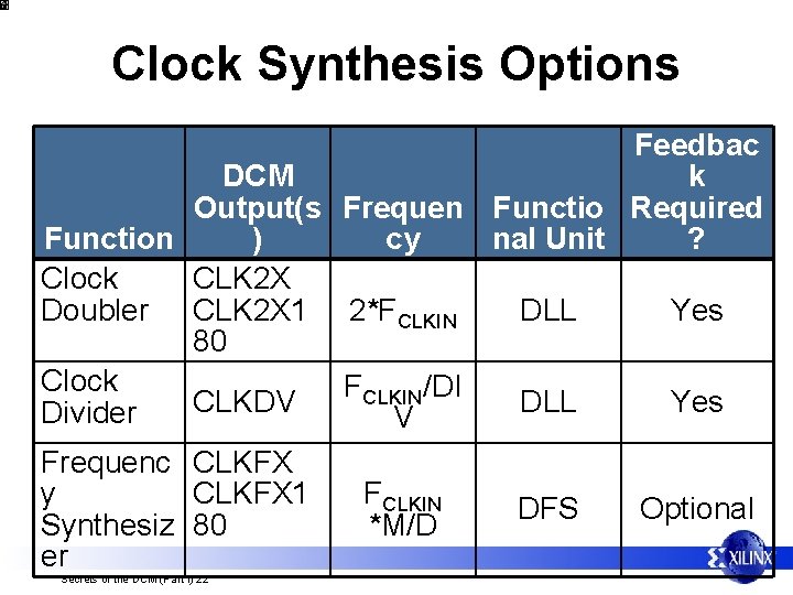
Clock Synthesis Options Feedbac DCM k Output(s Frequen Functio Required Function ) cy nal Unit ? Clock CLK 2 X Doubler CLK 2 X 1 2*FCLKIN DLL Yes 80 Clock FCLKIN/DI CLKDV DLL Yes Divider V Frequenc CLKFX y CLKFX 1 FCLKIN DFS Optional Synthesiz 80 *M/D er Secrets of the DCM (Part I) 22
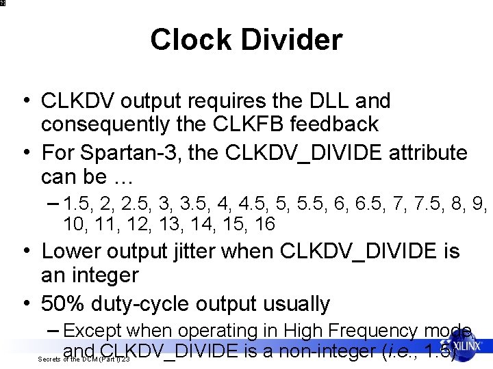
Clock Divider • CLKDV output requires the DLL and consequently the CLKFB feedback • For Spartan-3, the CLKDV_DIVIDE attribute can be … – 1. 5, 2, 2. 5, 3, 3. 5, 4, 4. 5, 5, 5. 5, 6, 6. 5, 7, 7. 5, 8, 9, 10, 11, 12, 13, 14, 15, 16 • Lower output jitter when CLKDV_DIVIDE is an integer • 50% duty-cycle output usually – Except when operating in High Frequency mode and CLKDV_DIVIDE is a non-integer (i. e. , 1. 5) Secrets of the DCM (Part I) 23
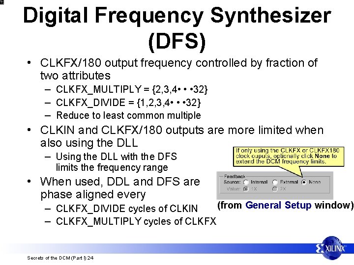
Digital Frequency Synthesizer (DFS) • CLKFX/180 output frequency controlled by fraction of two attributes – CLKFX_MULTIPLY = {2, 3, 4 • • • 32} – CLKFX_DIVIDE = {1, 2, 3, 4 • • • 32} – Reduce to least common multiple • CLKIN and CLKFX/180 outputs are more limited when also using the DLL – Using the DLL with the DFS limits the frequency range • When used, DDL and DFS are phase aligned every (from General Setup window) – CLKFX_DIVIDE cycles of CLKIN – CLKFX_MULTIPLY cycles of CLKFX Secrets of the DCM (Part I) 24
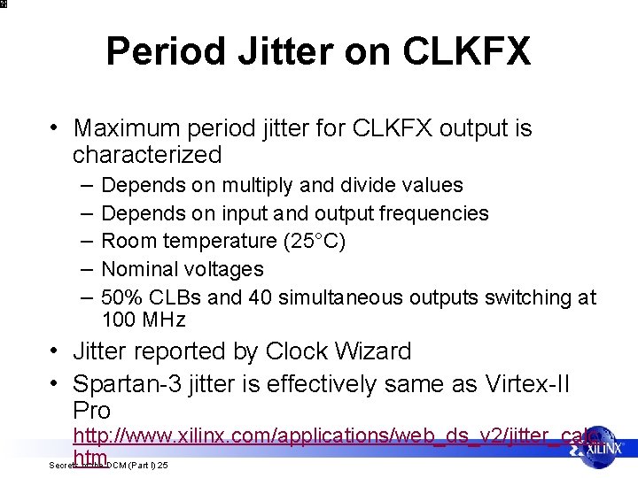
Period Jitter on CLKFX • Maximum period jitter for CLKFX output is characterized – – – Depends on multiply and divide values Depends on input and output frequencies Room temperature (25°C) Nominal voltages 50% CLBs and 40 simultaneous outputs switching at 100 MHz • Jitter reported by Clock Wizard • Spartan-3 jitter is effectively same as Virtex-II Pro http: //www. xilinx. com/applications/web_ds_v 2/jitter_calc. htm Secrets of the DCM (Part I) 25
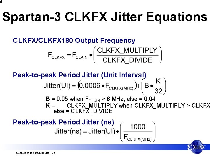
Spartan-3 CLKFX Jitter Equations CLKFX/CLKFX 180 Output Frequency Peak-to-peak Period Jitter (Unit Interval) B = 0. 05 when FCLKIN > 8 MHz, else = 0. 04 K= CLKFX_MULTIPLY when CLKFX_MULTIPLY > CLKFX else = CLKFX_DIVIDE Peak-to-peak Period Jitter (ns) Secrets of the DCM (Part I) 26
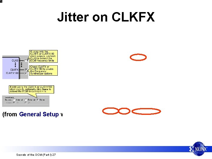
Jitter on CLKFX (from General Setup window) Secrets of the DCM (Part I) 27
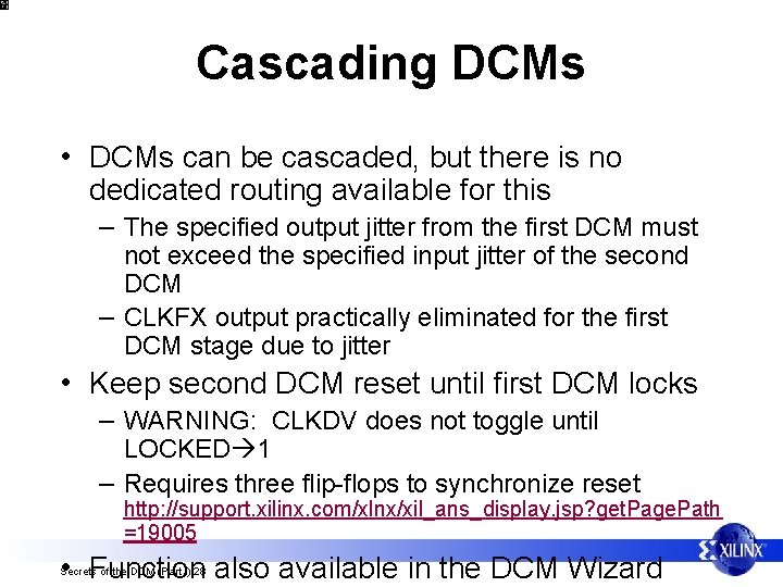
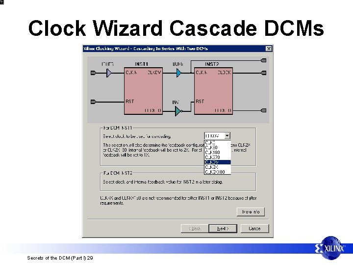
Cascading DCMs • DCMs can be cascaded, but there is no dedicated routing available for this – The specified output jitter from the first DCM must not exceed the specified input jitter of the second DCM – CLKFX output practically eliminated for the first DCM stage due to jitter • Keep second DCM reset until first DCM locks – WARNING: CLKDV does not toggle until LOCKED 1 – Requires three flip-flops to synchronize reset http: //support. xilinx. com/xlnx/xil_ans_display. jsp? get. Page. Path =19005 • Function also available in the DCM Wizard Secrets of the DCM (Part I) 28
Clock Wizard Cascade DCMs Secrets of the DCM (Part I) 29
Lesson Six System vs. Source Synchronous Design
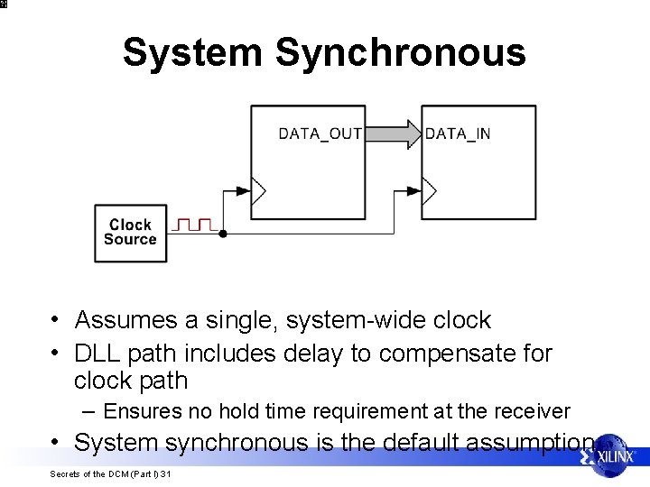
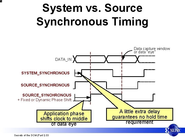
System Synchronous • Assumes a single, system-wide clock • DLL path includes delay to compensate for clock path – Ensures no hold time requirement at the receiver • System synchronous is the default assumption Secrets of the DCM (Part I) 31
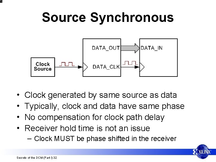
Source Synchronous • • Clock generated by same source as data Typically, clock and data have same phase No compensation for clock path delay Receiver hold time is not an issue – Clock MUST be phase shifted in the receiver Secrets of the DCM (Part I) 32
System vs. Source Synchronous Timing Data capture window or data “eye” DATA_IN SYSTEM_SYNCHRONOUS SOURCE_SYNCHRONOUS + Fixed or Dynamic Phase Shift Application phase shifts clock to middle of data eye Secrets of the DCM (Part I) 33 A little extra delay guarantees no hold time requirement
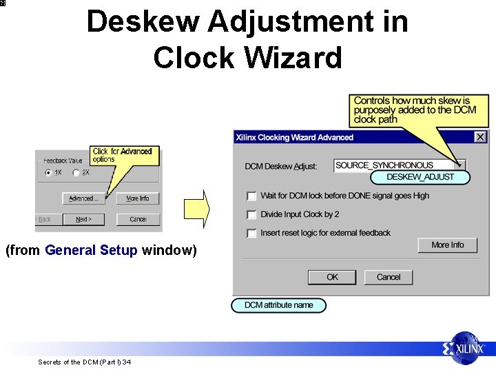
Deskew Adjustment in Clock Wizard (from General Setup window) Secrets of the DCM (Part I) 34
Lesson Seven Optional Divide by 2
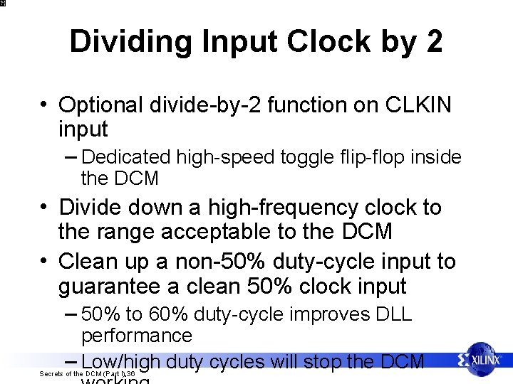
Dividing Input Clock by 2 • Optional divide-by-2 function on CLKIN input – Dedicated high-speed toggle flip-flop inside the DCM • Divide down a high-frequency clock to the range acceptable to the DCM • Clean up a non-50% duty-cycle input to guarantee a clean 50% clock input – 50% to 60% duty-cycle improves DLL performance – Low/high duty cycles will stop the DCM Secrets of the DCM (Part I) 36
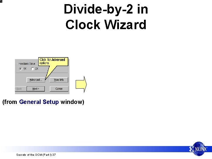
Divide-by-2 in Clock Wizard (from General Setup window) Secrets of the DCM (Part I) 37
Lesson Eight 622 Mbps Interface: Pulling it all together
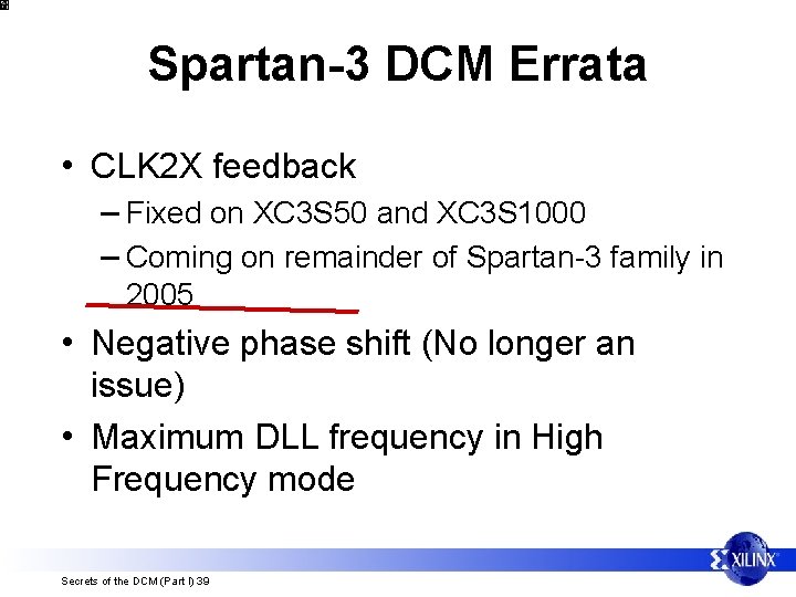
Spartan-3 DCM Errata • CLK 2 X feedback – Fixed on XC 3 S 50 and XC 3 S 1000 – Coming on remainder of Spartan-3 family in 2005 • Negative phase shift (No longer an issue) • Maximum DLL frequency in High Frequency mode Secrets of the DCM (Part I) 39
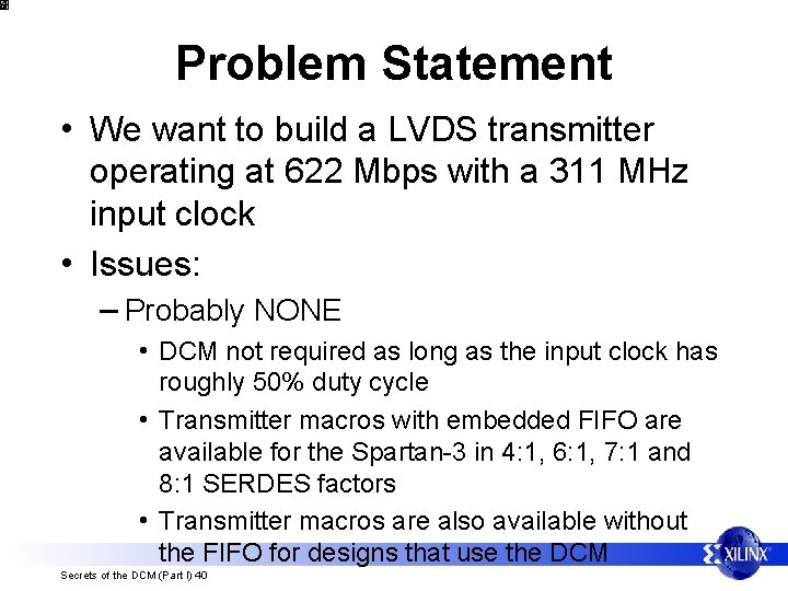
Problem Statement • We want to build a LVDS transmitter operating at 622 Mbps with a 311 MHz input clock • Issues: – Probably NONE • DCM not required as long as the input clock has roughly 50% duty cycle • Transmitter macros with embedded FIFO are available for the Spartan-3 in 4: 1, 6: 1, 7: 1 and 8: 1 SERDES factors • Transmitter macros are also available without the FIFO for designs that use the DCM Secrets of the DCM (Part I) 40
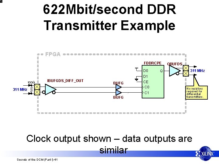
622 Mbit/second DDR Transmitter Example FPGA FDDRCPE D 0 100 W IBUFGDS_DIFF_OUT BUFG 311 MHz D 1 CE C 0 C 1 BUFG Q OBUFDS 311 MHz No resistors required for differential transmitters. Clock output shown – data outputs are similar Secrets of the DCM (Part I) 41
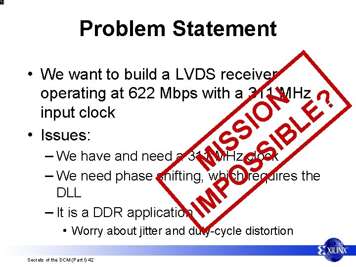
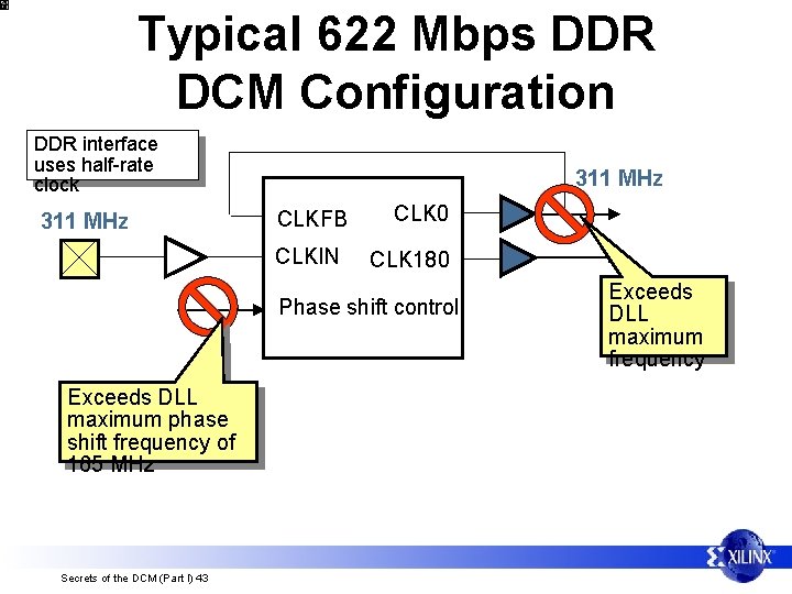
Problem Statement • We want to build a LVDS receiver operating at 622 Mbps with a 311 MHz input clock • Issues: N E? O L I S B I S I clock. S – We have and need a 311 MHz M S the – We need phase shifting, which requires O DLL P – It is a DDR application IM • Worry about jitter and duty-cycle distortion Secrets of the DCM (Part I) 42
Typical 622 Mbps DDR DCM Configuration DDR interface uses half-rate clock 311 MHz CLKFB CLKIN CLK 0 CLK 180 Phase shift control Exceeds DLL maximum phase shift frequency of 165 MHz Secrets of the DCM (Part I) 43 Exceeds DLL maximum frequency
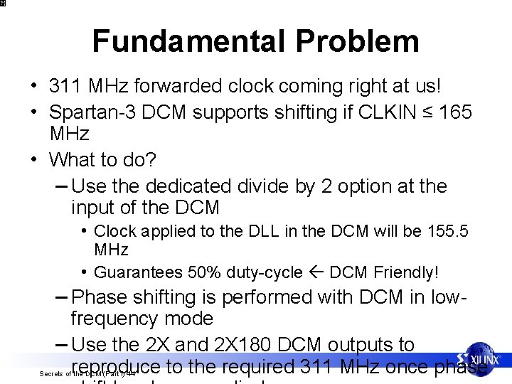
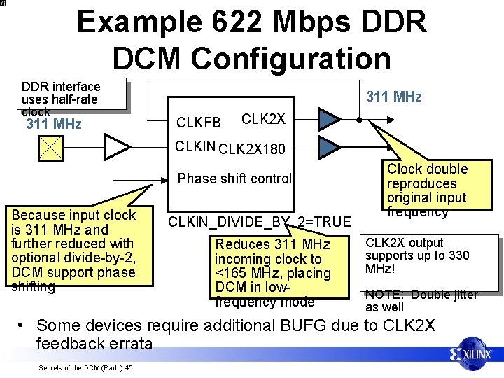
Fundamental Problem • 311 MHz forwarded clock coming right at us! • Spartan-3 DCM supports shifting if CLKIN ≤ 165 MHz • What to do? – Use the dedicated divide by 2 option at the input of the DCM • Clock applied to the DLL in the DCM will be 155. 5 MHz • Guarantees 50% duty-cycle DCM Friendly! – Phase shifting is performed with DCM in low- frequency mode – Use the 2 X and 2 X 180 DCM outputs to reproduce to the required 311 MHz once phase Secrets of the DCM (Part I) 44
Example 622 Mbps DDR DCM Configuration DDR interface uses half-rate clock 311 MHz CLKFB CLK 2 X CLKIN CLK 2 X 180 Phase shift control Because input clock is 311 MHz and further reduced with optional divide-by-2, DCM support phase shifting CLKIN_DIVIDE_BY_2=TRUE Reduces 311 MHz incoming clock to <165 MHz, placing DCM in lowfrequency mode Clock double reproduces original input frequency CLK 2 X output supports up to 330 MHz! NOTE: Double jitter as well • Some devices require additional BUFG due to CLK 2 X feedback errata Secrets of the DCM (Part I) 45
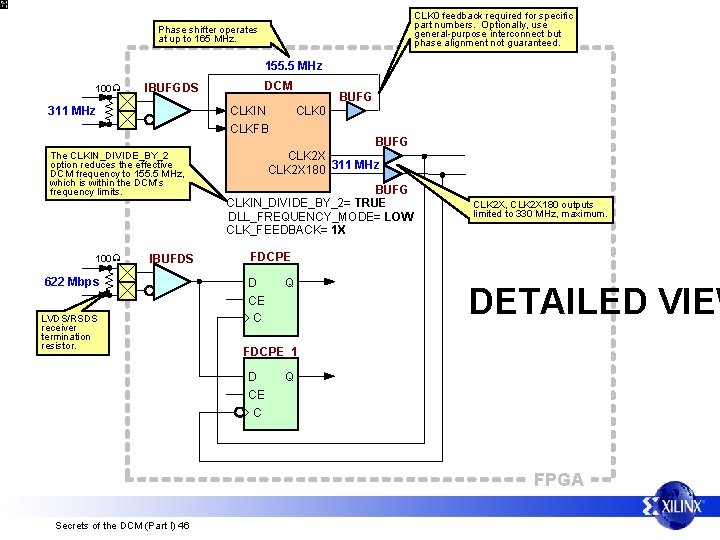
CLK 0 feedback required for specific part numbers. Optionally, use general-purpose interconnect but phase alignment not guaranteed. Phase shifter operates at up to 165 MHz. 155. 5 MHz 100 W 311 MHz CLKIN CLKFB The CLKIN_DIVIDE_BY_2 option reduces the effective DCM frequency to 155. 5 MHz, which is within the DCM’s frequency limits. 100 W DCM IBUFGDS IBUFDS 622 Mbps LVDS/RSDS receiver termination resistor. BUFG CLK 0 BUFG CLK 2 X 180 311 MHz BUFG CLKIN_DIVIDE_BY_2= TRUE DLL_FREQUENCY_MODE= LOW CLK_FEEDBACK= 1 X CLK 2 X, CLK 2 X 180 outputs limited to 330 MHz, maximum. FDCPE D CE C Q DETAILED VIEW FDCPE_1 D CE C Q FPGA Secrets of the DCM (Part I) 46
Problem Re-Statement • We want to build a LVDS receiver operating at 622 Mbps with a 311 MHz input clock • Issues solved : – Phase shifting is indirectly available at 311 MHz – Receiver macros are available for Spartan-3 at 1: 4, 1: 6, 1: 7 and 1: 8 SERDES factors – Setup and hold ‘eye’ parameters do still require characterization Secrets of the DCM (Part I) 47
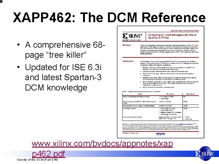
XAPP 462: The DCM Reference • A comprehensive 68 page “tree killer” • Updated for ISE 6. 3 i and latest Spartan-3 DCM knowledge www. xilinx. com/bvdocs/appnotes/xap p 462. pdf Secrets of the DCM (Part I) 48
Questions? gpd_apps@xilinx. com Secrets of the DCM (Part I) 49
Please Fill Out and Return the Feedback Forms! • Forms are in the back of your FAE conference book • Please return at back of the room Secrets of the DCM: Part 2 Steve Knapp ü ü ü Secrets of the DCM (Part I) 50 ! u o Y k n a h T
Jump Point • Lesson 4: Phase Shifting • Lesson 5: Frequency Synthesis • Lesson 6: System vs. Source Synchronous • Lesson 7: Optional CLKIN divide-by-2 • Lesson 8: Spartan-3 622 Mbps Design Example • Session Evaluation Forms Return to last slide viewe Secrets of the DCM (Part I) 51