Review of thin film deposition and etching techniques
- Slides: 38

Review of thin film deposition and etching techniques important for nanofabrication • • • Physical vapor deposition (PVD): evaporation and sputtering. Wet chemical etching. Plasma etching – reactive ion etching ICP and deep Si etching Stencil mask lithography Chemical vapor deposition (CVD, including LPCVD and PECVD): important forming “functional” materials, notably semiconducting materials. They are unimportant for structure fabrication where film quality is not a major concern. For example, Si and Si. O 2 can be used as a pattern transfer layer in the bi- or tri-layer resist scheme for easy liftoff, but they can be deposited by evaporation or sputtering. Of course, Si by evaporation won’t have any good semiconducting property. I rarely use CVD for my research. If I need wafers coated with LPCVD silicon nitride for membrane fabrication… I just buy them. ECE 730: Fabrication in the nanoscale: principles, technology and applications Instructor: Bo Cui, ECE, University of Waterloo; http: //ece. uwaterloo. ca/~bcui/ Textbook: Nanofabrication: principles, capabilities and limits, by Zheng Cui

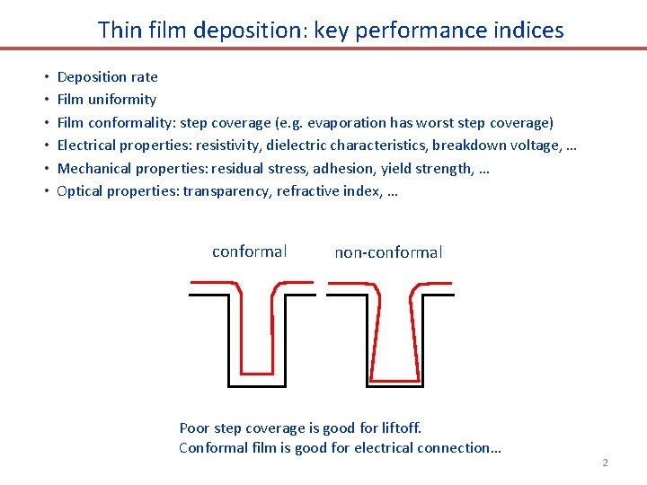
Thin film deposition: key performance indices • • • Deposition rate Film uniformity Film conformality: step coverage (e. g. evaporation has worst step coverage) Electrical properties: resistivity, dielectric characteristics, breakdown voltage, … Mechanical properties: residual stress, adhesion, yield strength, … Optical properties: transparency, refractive index, … conformal non-conformal Poor step coverage is good for liftoff. Conformal film is good for electrical connection… 2

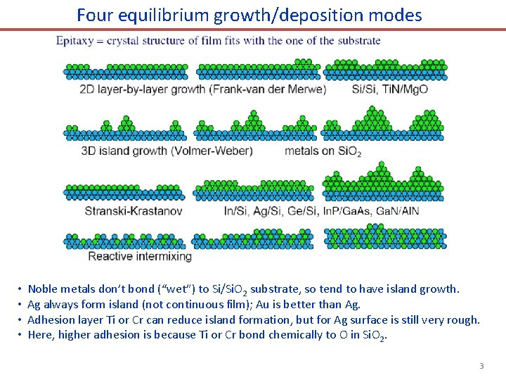
Four equilibrium growth/deposition modes • • Noble metals don’t bond (“wet”) to Si/Si. O 2 substrate, so tend to have island growth. Ag always form island (not continuous film); Au is better than Ag. Adhesion layer Ti or Cr can reduce island formation, but for Ag surface is still very rough. Here, higher adhesion is because Ti or Cr bond chemically to O in Si. O 2. 3

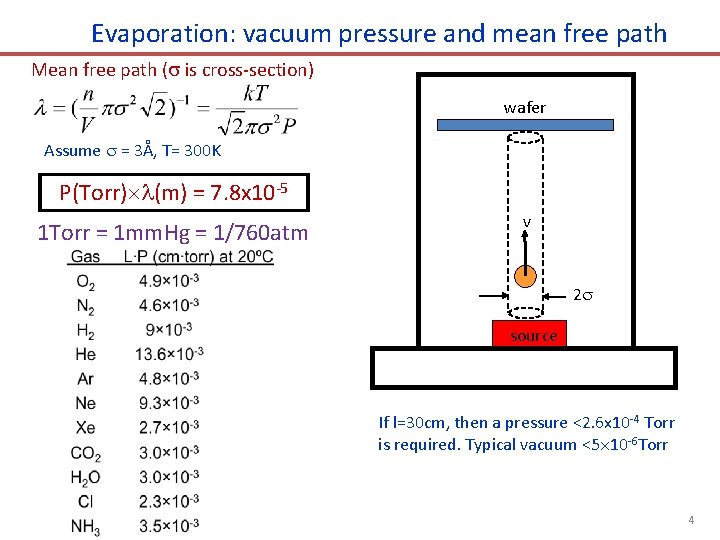
Evaporation: vacuum pressure and mean free path Mean free path ( is cross-section) wafer Assume = 3Å, T= 300 K P(Torr) (m) = 7. 8 x 10 -5 1 Torr = 1 mm. Hg = 1/760 atm v 2 source If l=30 cm, then a pressure <2. 6 x 10 -4 Torr is required. Typical vacuum <5 10 -6 Torr 4

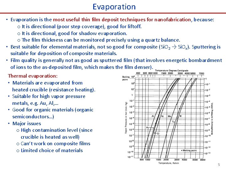
Evaporation • Evaporation is the most useful thin film deposit techniques for nanofabrication, because: o It is directional (poor step coverage), good for liftoff. o It is directional, good for shadow evaporation. o The film thickness can be monitored precisely using a quartz balance. • Best suitable for elemental materials, not so good for composite (Si. O 2 → Si. Ox). Sputtering is suitable for deposition of composite materials. • Film quality is generally not as good as sputtered film (that involves energetic bombardment of ions to the as-deposited film, which makes the film denser). Thermal evaporation: • Materials are evaporated from heated crucible (resistance heating). • Suitable for high vapor pressure metals, e. g. Au, Al, … • Good for organic materials (organic semiconductors…) • Major issues o High contamination level (since crucible is heated as well) o Can’t work on composite films o Limited choice of materials 5

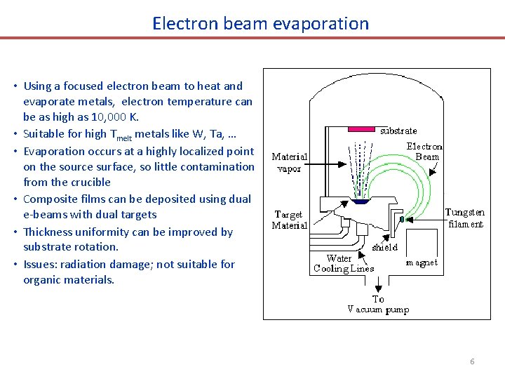
Electron beam evaporation • Using a focused electron beam to heat and evaporate metals, electron temperature can be as high as 10, 000 K. • Suitable for high Tmelt metals like W, Ta, … • Evaporation occurs at a highly localized point on the source surface, so little contamination from the crucible • Composite films can be deposited using dual e-beams with dual targets • Thickness uniformity can be improved by substrate rotation. • Issues: radiation damage; not suitable for organic materials. 6

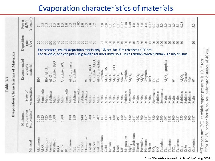
Evaporation characteristics of materials For research, typical deposition rate is only 1Å/sec, for film thickness <100 nm. For crucible, one can just use graphite for most materials, unless carbon contamination is a major issue. 7. From “Materials science of thin films” by Ohring, 2002.

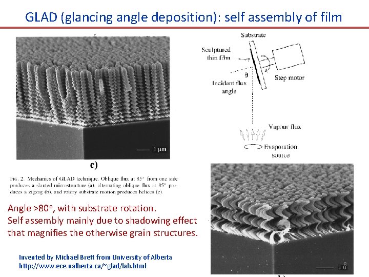
GLAD (glancing angle deposition): self assembly of film Angle >80 o, with substrate rotation. Self assembly mainly due to shadowing effect that magnifies the otherwise grain structures. Invented by Michael Brett from University of Alberta http: //www. ece. ualberta. ca/~glad/lab. html 8

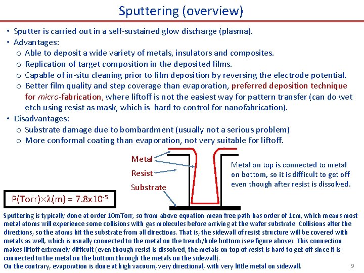
Sputtering (overview) • Sputter is carried out in a self-sustained glow discharge (plasma). • Advantages: o Able to deposit a wide variety of metals, insulators and composites. o Replication of target composition in the deposited films. o Capable of in-situ cleaning prior to film deposition by reversing the electrode potential. o Better film quality and step coverage than evaporation, preferred deposition technique for micro-fabrication, where liftoff is not the easiest way for pattern transfer (can do wet etch using resist as mask, which is hard to control for nanofabrication). • Disadvantages: o Substrate damage due to bombardment (usually not a serious problem) o More conformal coating than evaporation, not very suitable for liftoff. Metal Resist Substrate Metal on top is connected to metal on bottom, so it is difficult to get off even though after resist is dissolved. P(Torr) (m) = 7. 8 x 10 -5 Sputtering is typically done at order 10 m. Torr, so from above equation mean free path has order of 1 cm, which means most metal atoms will experience some collisions with gas molecules before arriving at the wafer substrate. Collisions alter the directions, so the atoms hit the substrate from all directions. That is, the sidewall of resist structure will be covered with metals as well, which is usually connected to the metal on the trench/hole bottom (see figure above). This connection makes liftoff extremely difficult (even though resist is dissolved, the metals on top of resist is hard to get off since it is connected to the metal on the bottom through the metals on the sidewall). 9 On the contrary, evaporation is done at high vacuum, very directional, with very little metal on sidewall.

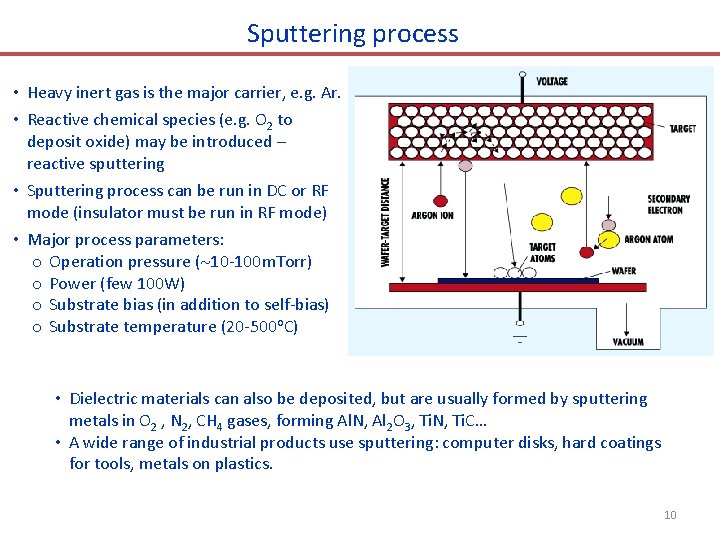
Sputtering process • Heavy inert gas is the major carrier, e. g. Ar. • Reactive chemical species (e. g. O 2 to deposit oxide) may be introduced – reactive sputtering • Sputtering process can be run in DC or RF mode (insulator must be run in RF mode) • Major process parameters: o Operation pressure ( 10 -100 m. Torr) o Power (few 100 W) o Substrate bias (in addition to self-bias) o Substrate temperature (20 -500 o. C) • Dielectric materials can also be deposited, but are usually formed by sputtering metals in O 2 , N 2, CH 4 gases, forming Al. N, Al 2 O 3, Ti. N, Ti. C… • A wide range of industrial products use sputtering: computer disks, hard coatings for tools, metals on plastics. 10

Review of thin film deposition and etching techniques important for nanofabrication • • • Physical vapor deposition (PVD): evaporation and sputtering. Wet chemical etching. Plasma etching – reactive ion etching ICP and deep Si etching Stencil mask lithography

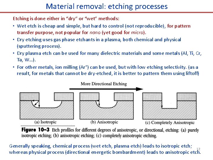
Material removal: etching processes Etching is done either in “dry” or “wet” methods: • Wet etch is cheap and simple, but hard to control (not reproducible), for pattern transfer purpose, not popular for nano (yet good for micro). • Dry etching uses gas phase etchants in a plasma, both chemical and physical (sputtering process). • Dry plasma etch can be used for many dielectric materials and some metals (Al, Ti, Cr, Ta, W…). • For other metals, ion milling (Ar+) can be used, but with low etching selectivity. (as a result, for metals that cannot be dry-etched, it is better to pattern them using liftoff) Generally speaking, chemical process (wet etch, plasma etch) leads to isotropic etch; 12 whereas physical process (directional energetic bombardment) leads to anisotropic etch.

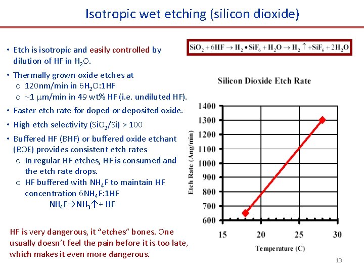
Isotropic wet etching (silicon dioxide) • Etch is isotropic and easily controlled by dilution of HF in H 2 O. • Thermally grown oxide etches at o 120 nm/min in 6 H 2 O: 1 HF o 1 m/min in 49 wt% HF (i. e. undiluted HF). • Faster etch rate for doped or deposited oxide. • High etch selectivity (Si. O 2/Si) > 100 • Buffered HF (BHF) or buffered oxide etchant (BOE) provides consistent etch rates o In regular HF etches, HF is consumed and the etch rate drops. o HF buffered with NH 4 F to maintain HF concentration 6 NH 4 F: 1 HF NH 4 F→NH 3↑+ HF HF is very dangerous, it “etches” bones. One usually doesn’t feel the pain before it is too late, which makes it even more dangerous. 13

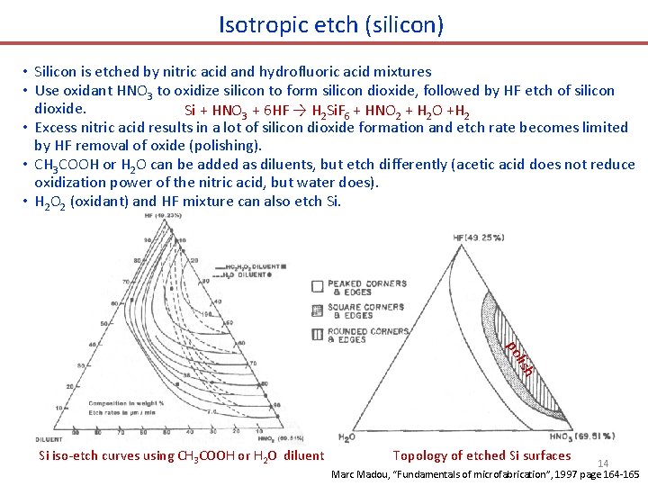
Isotropic etch (silicon) • Silicon is etched by nitric acid and hydrofluoric acid mixtures • Use oxidant HNO 3 to oxidize silicon to form silicon dioxide, followed by HF etch of silicon dioxide. Si + HNO 3 + 6 HF → H 2 Si. F 6 + HNO 2 + H 2 O +H 2 • Excess nitric acid results in a lot of silicon dioxide formation and etch rate becomes limited by HF removal of oxide (polishing). • CH 3 COOH or H 2 O can be added as diluents, but etch differently (acetic acid does not reduce oxidization power of the nitric acid, but water does). • H 2 O 2 (oxidant) and HF mixture can also etch Si. lish po Si iso-etch curves using CH 3 COOH or H 2 O diluent Topology of etched Si surfaces 14 Marc Madou, “Fundamentals of microfabrication”, 1997 page 164 -165

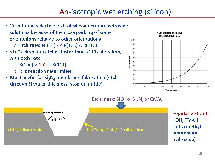
An-isotropic wet etching (silicon) • Orientation selective etch of silicon occur in hydroxide solutions because of the close packing of some orientations relative to other orientations o Etch rate: R(111) << R(100) < R(110) • <100> direction etches faster than <111> direction, with etch rate o R(100) > 100 R(111) o It is reaction rate limited • Most useful for Si 3 N 4 membrane fabrication (etch through Si wafer thickness, stop at nitride). Etch mask: Si. O 2 or Si 3 N 4 or Cr/Au (100) Silicon wafer Etch “stops” at (111) direction Popular etchant: KOH, TMAH (tetra methyl ammonium hydroxide) 15

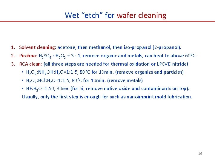
Wet “etch” for wafer cleaning 1. Solvent cleaning: acetone, then methanol, then iso-propanol (2 -propanol). 2. Pirahna: H 2 SO 4 : H 2 O 2 = 3 : 1, remove organic and metals, can heat to above 60 o. C. 3. RCA clean: (all three steps are needed for thermal oxidation or LPCVD nitride) • H 2 O 2: NH 4 OH: H 2 O=1: 1: 5, 80 o. C for 10 min. (remove organics and particles) • H 2 O 2: HCl: H 2 O=1: 1: 5, 80 o. C for 10 min. (remove metals) • HF: H 2 O=1: 50, 30 sec (for Si, remove native oxide and contaminants on top). Usually, only the first step is enough for such as nanoimprint mold fabrication. 16

Review of thin film deposition and etching techniques important for nanofabrication • • • Physical vapor deposition (PVD): evaporation and sputtering. Wet chemical etching. Plasma etching – reactive ion etching (RIE) ICP and deep Si etching Stencil mask lithography

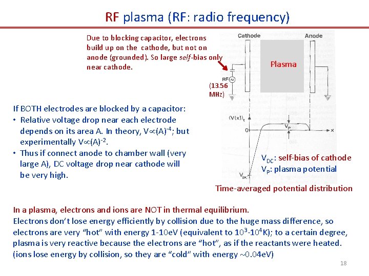
RF plasma (RF: radio frequency) Due to blocking capacitor, electrons build up on the cathode, but not on anode (grounded). So large self-bias only near cathode. Plasma (13. 56 MHz) If BOTH electrodes are blocked by a capacitor: • Relative voltage drop near each electrode depends on its area A. In theory, V (A)-4; but experimentally V (A)-2. • Thus if connect anode to chamber wall (very large A), DC voltage drop near cathode will be very high. VDC: self-bias of cathode VP: plasma potential Time-averaged potential distribution In a plasma, electrons and ions are NOT in thermal equilibrium. Electrons don’t lose energy efficiently by collision due to the huge mass difference, so electrons are very “hot” with energy 1 -10 e. V (equivalent to 103 -104 K); to a certain degree, plasma is very reactive because the electrons are “hot”, as if the reactants were heated. (ions lose energy by collision, so they are “cold” with energy 0. 04 e. V) 18

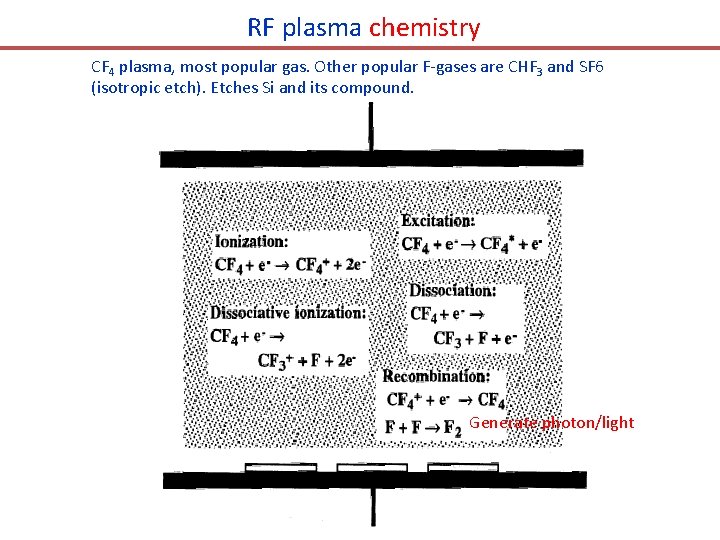
RF plasma chemistry CF 4 plasma, most popular gas. Other popular F-gases are CHF 3 and SF 6 (isotropic etch). Etches Si and its compound. Generate photon/light

RF plasma chemistry • In a plasma, reactive neutral chemical species (free radicals, e. g. F atoms or molecular species such as CF 3) are mainly responsible for the chemical reaction partly due to their great numbers compared to ions. • Those free radicals are more abundant than ions because: 1) they are generated at lower threshold energy (e. g. <8 e. V; in comparison, Ar is ionized at 15. 7 e. V); and 2) they (uncharged radicals) have longer lifetime in the plasma. • The neutral radicals arrive at cathode surface by diffusion (so non-directional). • Charged ions are accelerated to the cathode due to self-bias. (Unless with very high energy of >100 e. V as in ion beam etching), ion itself doesn’t contribute significantly to the chemical reaction mostly due to its very low concentration, but ion bombardment can greatly enhance the chemical reaction in reactive ion etching (RIE). • In RIE, ion energy is low 10 e. V due to collision energy loss. The name reactive “ion” etching is very misleading since ions don’t contribute directly to etching. 20

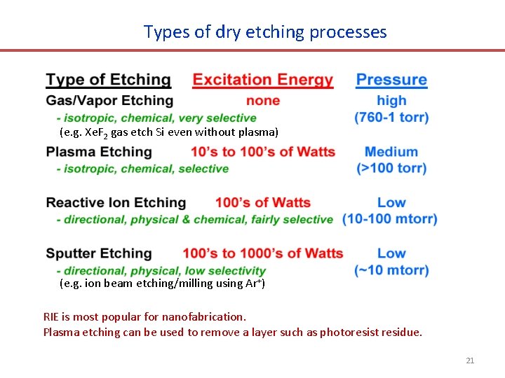
Types of dry etching processes (e. g. Xe. F 2 gas etch Si even without plasma) (e. g. ion beam etching/milling using Ar+) RIE is most popular for nanofabrication. Plasma etching can be used to remove a layer such as photoresist residue. 21

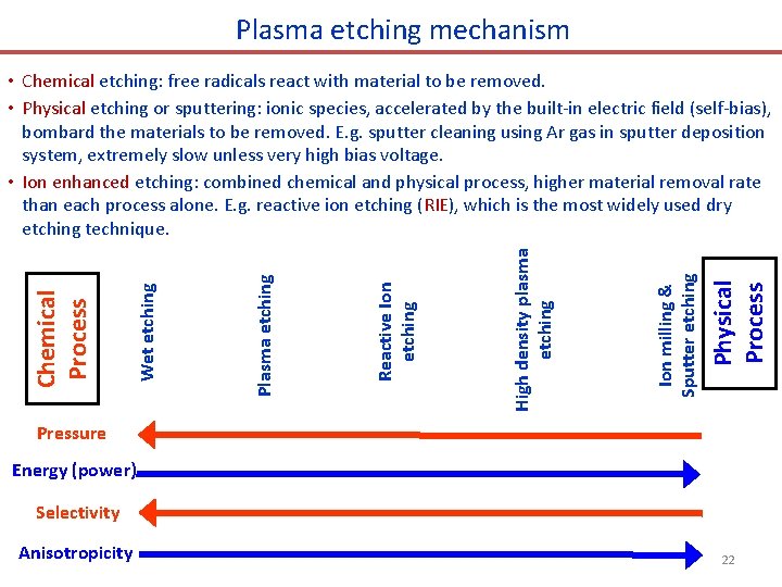
Plasma etching mechanism Physical Process Ion milling & Sputter etching High density plasma etching Reactive Ion etching Plasma etching Wet etching Chemical Process • Chemical etching: free radicals react with material to be removed. • Physical etching or sputtering: ionic species, accelerated by the built-in electric field (self-bias), bombard the materials to be removed. E. g. sputter cleaning using Ar gas in sputter deposition system, extremely slow unless very high bias voltage. • Ion enhanced etching: combined chemical and physical process, higher material removal rate than each process alone. E. g. reactive ion etching (RIE), which is the most widely used dry etching technique. Pressure Energy (power) Selectivity Anisotropicity 22

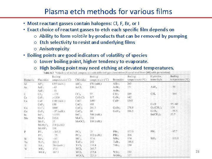
Plasma etch methods for various films • Most reactant gasses contain halogens: Cl, F, Br, or I • Exact choice of reactant gasses to etch each specific film depends on o Ability to form volatile by-products that can be removed by pumping o Etch selectivity to resist and underlying films o Anisotropicity • Boiling points are good indicators of volatility of species o Lower boiling point, higher tendency to evaporate. o High boiling point may need etching at elevated temperatures. 23

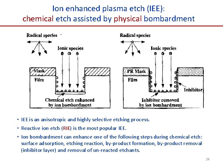
Ion enhanced plasma etch (IEE): chemical etch assisted by physical bombardment • IEE is an anisotropic and highly selective etching process. • Reactive ion etch (RIE) is the most popular IEE. • Ion bombardment can enhance one of the following steps during chemical etch: surface adsorption, etching reaction, by-product formation, by-product removal (inhibitor layer) and removal of un-reacted etchants. 24

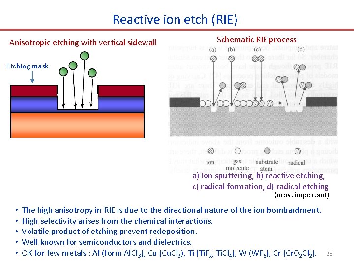
Reactive ion etch (RIE) Anisotropic etching with vertical sidewall Schematic RIE process Etching mask a) Ion sputtering, b) reactive etching, c) radical formation, d) radical etching (most important) • • • The high anisotropy in RIE is due to the directional nature of the ion bombardment. High selectivity arises from the chemical interactions. Volatile product of etching prevent redeposition. Well known for semiconductors and dielectrics. OK for few metals : Al (form Al. Cl 3), Cu (Cu. Cl 2), Ti (Ti. Fx, Ti. Cl 4), W (WF 6), Cr (Cr. O 2 Cl 2). 25

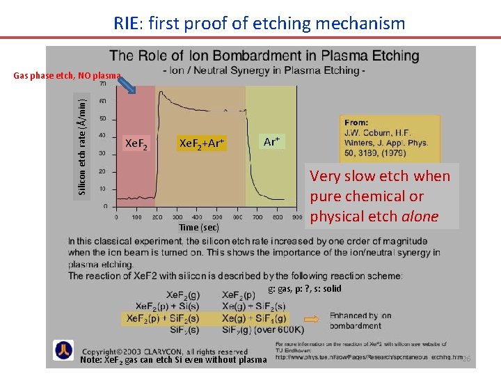
RIE: first proof of etching mechanism Silicon etch rate (Å/min) Gas phase etch, NO plasma Xe. F 2+Ar+ Time (sec) Very slow etch when pure chemical or physical etch alone g: gas, p: ? , s: solid Note: Xe. F 2 gas can etch Si even without plasma 26

Anisotropy due to ion bombardment • • Anisotropic etch with vertical sidewall is desired for micro- and nano-fabrication. But directional ion bombardment doesn’t always lead to noticeable anisotropic etch. For instance, SF 6 etch of Si is pretty isotropic with large undercut like wet etch. To achieve anisotropy, there are two mechanisms: o Energy-driven anisotropy: bombardment by ions disrupts an un-reactive substrate and causes damages such as dangling bonds and dislocations, resulting in a substrate more reactive towards etchant species (electrons or photons can also induce surface activation). o Inhibitor-driven anisotropy: in this case etching leads to the production of a surface covering agent (a passivation/inhibition layer). Ion bombardment removes this layer from horizontal surface (vertical surface - sidewall remain passivated), and reaction with neutrals proceed on these un-passivated surfaces only. E. g. RIE of Si. O 2 using CHF 3 gases to form fluorocarbon passivation layer. 27

Review of thin film deposition and etching techniques important for nanofabrication • • • Physical vapor deposition (PVD): evaporation and sputtering. Wet chemical etching. Plasma etching – reactive ion etching ICP and deep Si etching Stencil mask lithography

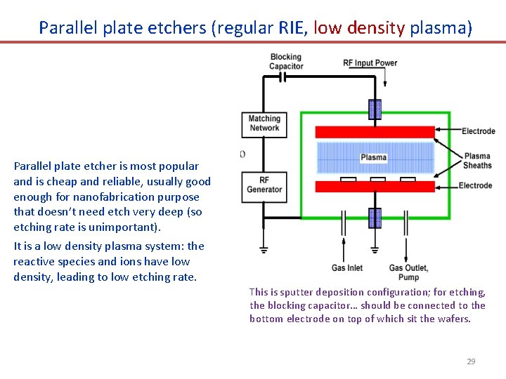
Parallel plate etchers (regular RIE, low density plasma) Parallel plate etcher is most popular and is cheap and reliable, usually good enough for nanofabrication purpose that doesn’t need etch very deep (so etching rate is unimportant). It is a low density plasma system: the reactive species and ions have low density, leading to low etching rate. This is sputter deposition configuration; for etching, the blocking capacitor… should be connected to the bottom electrode on top of which sit the wafers. 29

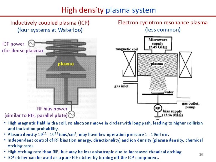
High density plasma system Inductively coupled plasma (ICP) (four systems at Waterloo) Electron cyclotron resonance plasma (less common) ICP power (for dense plasma) plasma RF bias power (similar to RIE, parallel plate) • High magnetic field in the coil, so electrons move in circles with long path, leading to higher collision and ionization probability. • Plasma density 1011 - 1012 ions/cm 3; may have low operation pressure 1 - 10 m. Torr. • Independent control of RF bias (ion energy, directionality) and ion density (plasma density, chemical etching rate). • High etching rate than RIE, but may be less anisotropic due to increased chemical etching. 30 • ICP etcher can be used as a pure RIE etcher by turning off the ICP component.

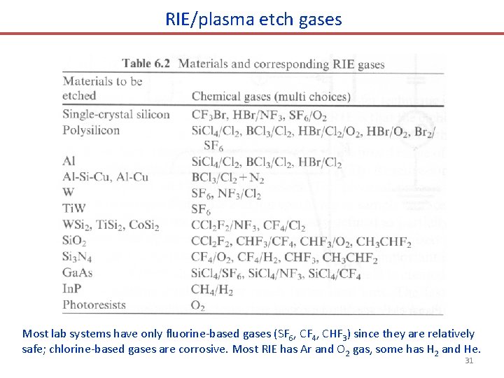
RIE/plasma etch gases Most lab systems have only fluorine-based gases (SF 6, CF 4, CHF 3) since they are relatively safe; chlorine-based gases are corrosive. Most RIE has Ar and O 2 gas, some has H 2 and He. 31

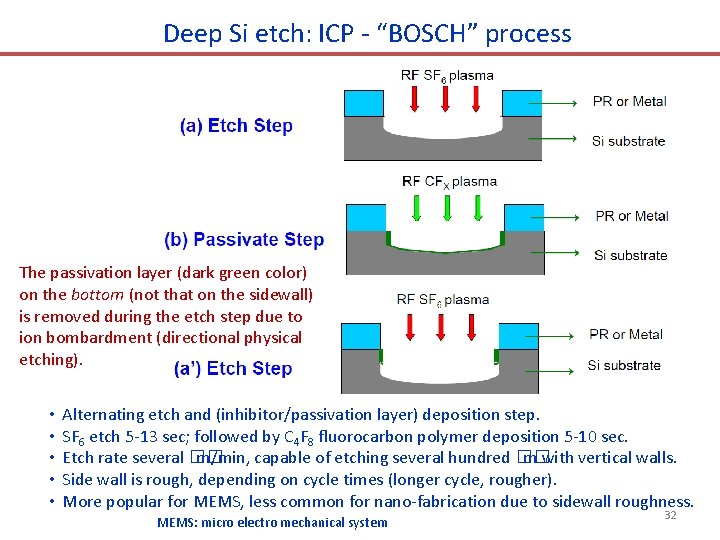
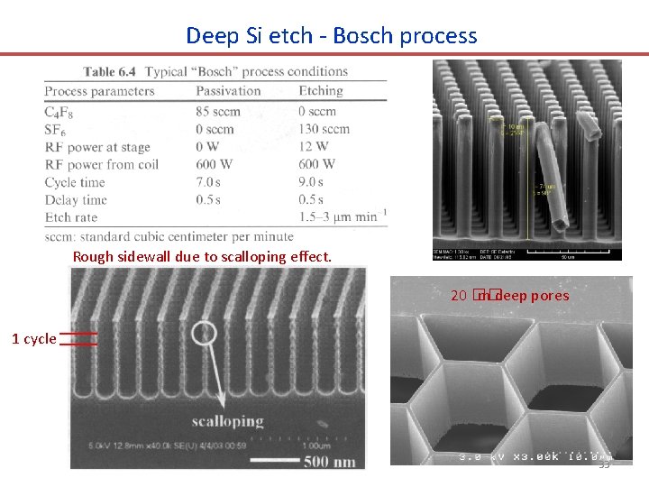
Deep Si etch: ICP - “BOSCH” process The passivation layer (dark green color) on the bottom (not that on the sidewall) is removed during the etch step due to ion bombardment (directional physical etching). • • • Alternating etch and (inhibitor/passivation layer) deposition step. SF 6 etch 5 -13 sec; followed by C 4 F 8 fluorocarbon polymer deposition 5 -10 sec. Etch rate several �� m/min, capable of etching several hundred �� m with vertical walls. Side wall is rough, depending on cycle times (longer cycle, rougher). More popular for MEMS, less common for nano-fabrication due to sidewall roughness. MEMS: micro electro mechanical system 32

Deep Si etch - Bosch process Rough sidewall due to scalloping effect. 20 �� m deep pores 1 cycle 33

Review of thin film deposition and etching techniques important for nanofabrication • • • Physical vapor deposition (PVD): evaporation and sputtering. Wet chemical etching. Plasma etching – reactive ion etching ICP and deep Si etching Stencil mask lithography

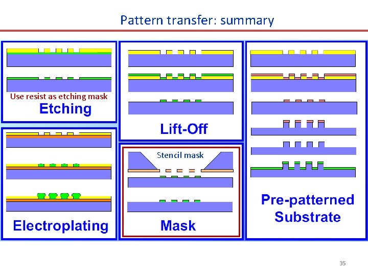
Pattern transfer: summary Use resist as etching mask Stencil mask 35

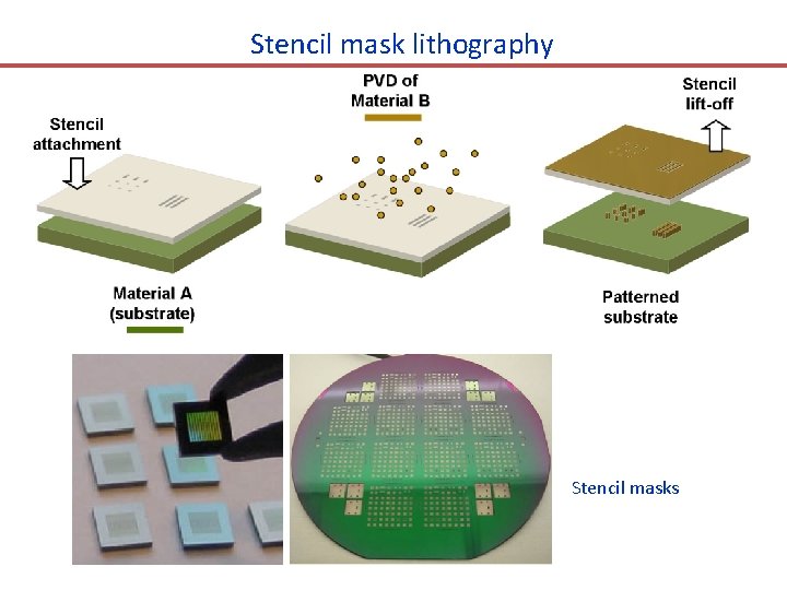
Stencil mask lithography Stencil masks

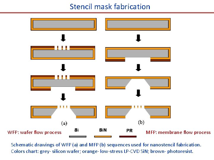
Stencil mask fabrication WFP: wafer flow process MFP: membrane flow process Schematic drawings of WFP (a) and MFP (b) sequences used for nanostencil fabrication. Colors chart: grey- silicon wafer; orange- low-stress LP-CVD Si. N; brown- photoresist.

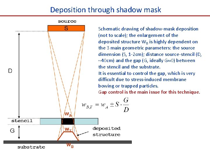
Deposition through shadow mask Schematic drawing of shadow-mask deposition (not to scale); the enlargement of the deposited structure WB is highly dependent on the 3 main geometric parameters: the source dimension (S, 1 -2 cm); distance source-stencil (D, 40 cm) and the gap (G, ideally G 0) between the stencil and the substrate. It is essential to control the gap, which is very difficult due to stress-induced membrane bowing or trapped particles. Gap control is the main issue for this technique.