Register Files and Memories ECE 554 Digital Engineering
- Slides: 47

Register Files and Memories ECE 554 Digital Engineering Laboratory C. R. Kime 2/18/2002 ECE 554 - Digital Engineering Laboratory

Register Files and Memories Register Files l l l Issues and Objectives Register File Concepts Implementation of Register Files Workarounds For Xilinx FPGAs Bottom Line Memories l l Timing Issues Width Expansion ECE 554 - Digital Engineering Laboratory 2

Issues and Objectives Issues l l ECE 554 projects require a broad range of register file and memory configurations ECE 554 lab boards provide very limited structures for implementing register files and memories. Objectives: l To develop techniques for implementing a broad range of register file and memory configurations by using with available lab board structures ECE 554 - Digital Engineering Laboratory 3

Register File Concepts Register file environments l l Non-Pipelined Register File Configurations l l l Address Ports Data Ports Control Ports Timing l l Latch Flip-flop ECE 554 - Digital Engineering Laboratory 4

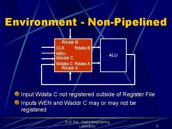
Environment - Non-Pipelined RAddr B CLK Rdata B WEn WAddr C Wdata C Rdata A RAddr A ALU Input Wdata C not registered outside of Register File Inputs WEN and Waddr C may or may not be registered ECE 554 - Digital Engineering Laboratory 5

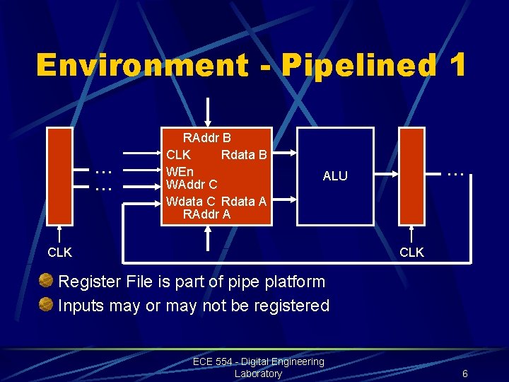
Environment - Pipelined 1. . . RAddr B CLK Rdata B WEn WAddr C Wdata C Rdata A RAddr A . . . ALU CLK Register File is part of pipe platform Inputs may or may not be registered ECE 554 - Digital Engineering Laboratory 6

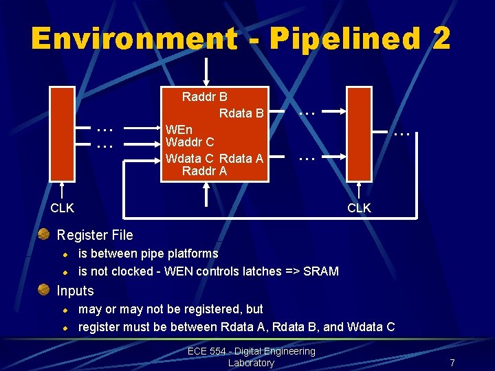
Environment - Pipelined 2. . . Raddr B Rdata B WEn Waddr C Wdata C Rdata A Raddr A . . CLK Register File l l is between pipe platforms is not clocked - WEN controls latches => SRAM Inputs l l may or may not be registered, but register must be between Rdata A, Rdata B, and Wdata C ECE 554 - Digital Engineering Laboratory 7

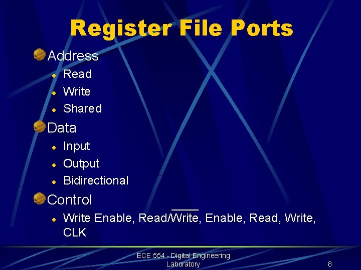
Register File Ports Address l l l Read Write Shared Data l l l Input Output Bidirectional Control l Write Enable, Read/Write, Enable, Read, Write, CLK ECE 554 - Digital Engineering Laboratory 8

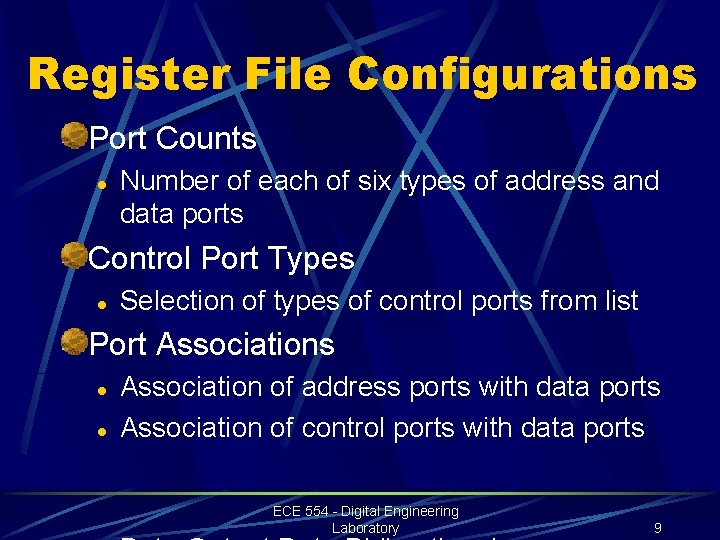
Register File Configurations Port Counts l Number of each of six types of address and data ports Control Port Types l Selection of types of control ports from list Port Associations l l Association of address ports with data ports Association of control ports with data ports ECE 554 - Digital Engineering Laboratory 9

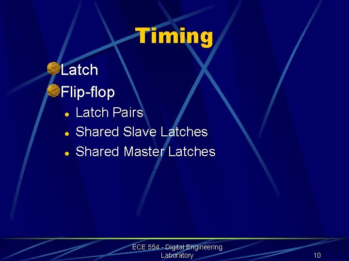
Timing Latch Flip-flop l l l Latch Pairs Shared Slave Latches Shared Master Latches ECE 554 - Digital Engineering Laboratory 10

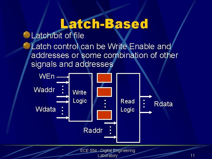
Latch-Based Latch/bit of file Latch control can be Write Enable and addresses or some combination of other signals and addresses WEn Rdata . . . Raddr Read Logic . . . Write Logic . . . Wdata . . . Waddr ECE 554 - Digital Engineering Laboratory 11

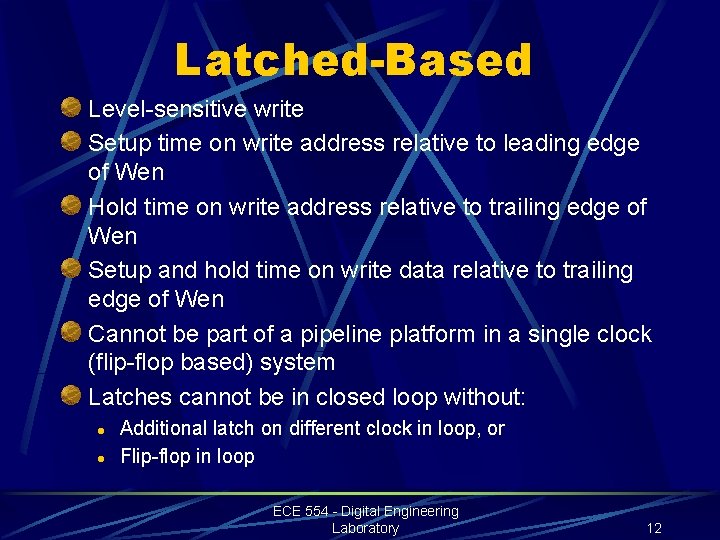
Latched-Based Level-sensitive write Setup time on write address relative to leading edge of Wen Hold time on write address relative to trailing edge of Wen Setup and hold time on write data relative to trailing edge of Wen Cannot be part of a pipeline platform in a single clock (flip-flop based) system Latches cannot be in closed loop without: l l Additional latch on different clock in loop, or Flip-flop in loop ECE 554 - Digital Engineering Laboratory 12

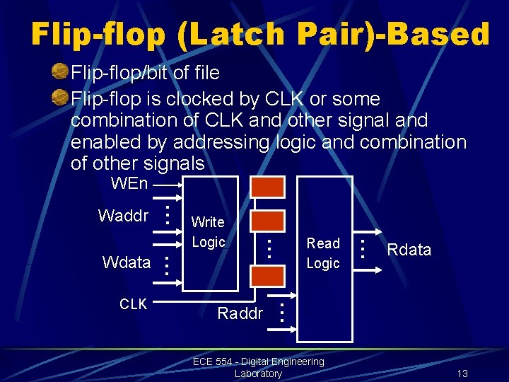
Flip-flop (Latch Pair)-Based Flip-flop/bit of file Flip-flop is clocked by CLK or some combination of CLK and other signal and enabled by addressing logic and combination of other signals WEn . . . Raddr Read Logic Rdata . . . CLK Write Logic . . . Wdata . . . Waddr ECE 554 - Digital Engineering Laboratory 13

Flip-flop (Latch Pair)-Based Write Logic adds setup-time to that for flipflops Read Logic adds propagation delay to that for flip-flops Acts like positive pulse master-slave or negative-edge triggered flip-flop register file with above delays added ECE 554 - Digital Engineering Laboratory 14

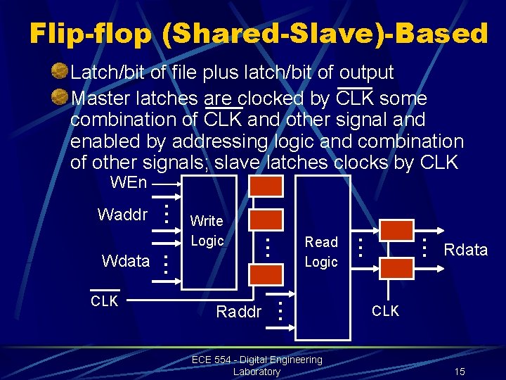
Flip-flop (Shared-Slave)-Based Latch/bit of file plus latch/bit of output Master latches are clocked by CLK some combination of CLK and other signal and enabled by addressing logic and combination of other signals; slave latches clocks by CLK WEn . . . ECE 554 - Digital Engineering Laboratory . . . Raddr Read Logic . . . CLK Write Logic . . . Wdata . . . Waddr Rdata CLK 15

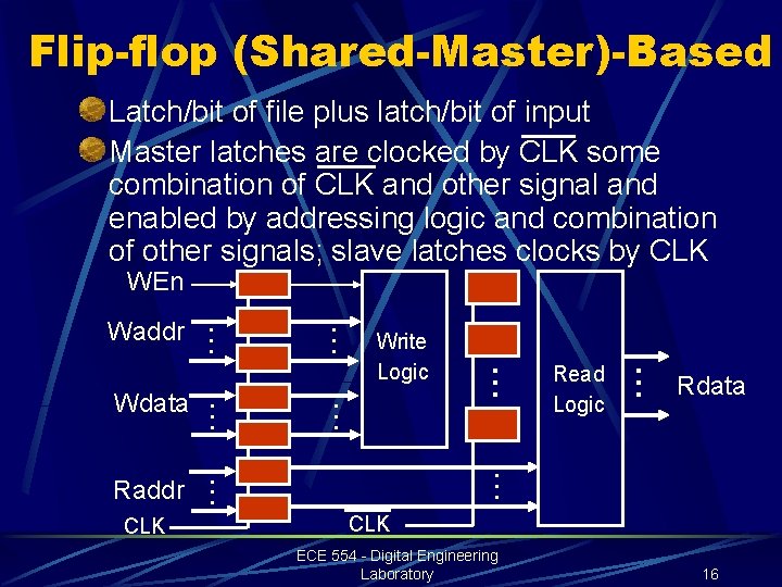
Flip-flop (Shared-Master)-Based Latch/bit of file plus latch/bit of input Master latches are clocked by CLK some combination of CLK and other signal and enabled by addressing logic and combination of other signals; slave latches clocks by CLK WEn . . . Read Logic Rdata . . . CLK . . . Raddr Write Logic . . . Wdata . . . Waddr CLK ECE 554 - Digital Engineering Laboratory 16

Implementation of Register Files Custom VLSI SRAM Classic SRAM Xilinx Virtex SRAM l l Specifications Shortcomings ECE 554 - Digital Engineering Laboratory 17

Custom VLSI SRAM Is the most flexible of all implementation techniques Can be used to implement any combination of variants discussed l l Latch-based straightforward; needs additional rank of latches to do flip-flopbased Short of performance issues due to capacitance, can implement any port configuration in a singe storage element array. ECE 554 - Digital Engineering Laboratory 18

Classic SRAM Has single RWaddr port, single Wdata port, and single Rdata port and is latch-based. l l Due to single address port, can handle only one R or W access per clock cycle Since latch-based, cannot serve as part of a pipe platform hence Pipelined 2 form Expansion to n R address/data ports l Place n SRAMs in parallel with the write accomplished by: l l Applying same address to all Rwaddr, and Wiring together all Wdata ports Expansion to m W address/data ports l l Add an m-way multiplexer to address port Use a clock that is m times CLK and multiplex the writes over m clocks ECE 554 - Digital Engineering Laboratory 19

Classic SRAM (Continued) l l Addresses must be switched on positive clock edge WEn must be generated from negative clock edge and positive clock edge Expansion to m W address/data ports and n R address/data ports l Doing both expansions above l l Using (m +1)-way multiplexer, and A clock that is (m + 1) times CLK Virtex Distributed Select. RAM l l The SRAM capability provided in CLBs Can be used with expansion methods here in classic asynchronous SRAM mode or some synchronous modes Getting reliable timing is tricky - may require more complex clocking! See Old Register File writeup on website ECE 554 - Digital Engineering Laboratory 20

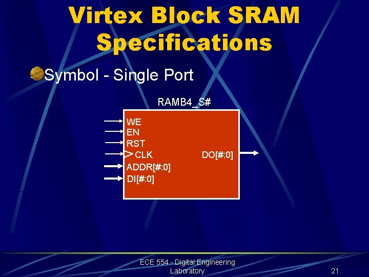
Virtex Block SRAM Specifications Symbol - Single Port RAMB 4_S# WE EN RST CLK ADDR[#: 0] DI[#: 0] DO[#: 0] ECE 554 - Digital Engineering Laboratory 21

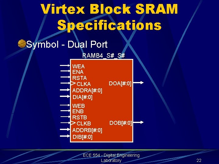
Virtex Block SRAM Specifications Symbol - Dual Port RAMB 4_S#_S# WEA ENA RSTA CLKA ADDRA[#: 0] DIA[#: 0] DOA[#: 0] WEB ENB RSTB CLKB ADDRB[#: 0] DIB[#: 0] DOB[#: 0] ECE 554 - Digital Engineering Laboratory 22

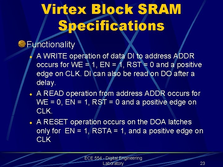
Virtex Block SRAM Specifications Functionality l l l A WRITE operation of data DI to address ADDR occurs for WE = 1, EN = 1, RST = 0 and a positive edge on CLK. DI can also be read on DO after a delay. A READ operation from address ADDR occurs for WE = 0, EN = 1, RST = 0 and a positive edge on CLK. A RESET operation occurs on the DOA latches only for EN = 1, RSTA = 1, and a positive edge on CLK ECE 554 - Digital Engineering Laboratory 23

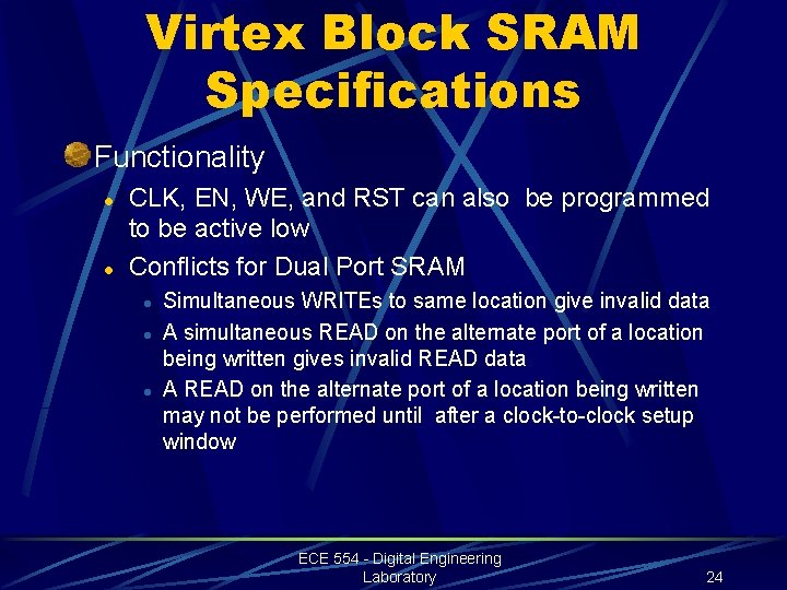
Virtex Block SRAM Specifications Functionality l l CLK, EN, WE, and RST can also be programmed to be active low Conflicts for Dual Port SRAM l l l Simultaneous WRITEs to same location give invalid data A simultaneous READ on the alternate port of a location being written gives invalid READ data A READ on the alternate port of a location being written may not be performed until after a clock-to-clock setup window ECE 554 - Digital Engineering Laboratory 24

Virtex Block SRAM Specifications Functionality - Timing l l l EN, WE, RST, ADDR, DI are captured on the positive edge of CLK in registers (unclear whether latches or flip-flops) WRITEs into the SRAM latch array occur later due to internal timing logic READs (including those associated with writes) occur later due to internal timing logic ECE 554 - Digital Engineering Laboratory 25

Virtex Block SRAM Shortcomings Using Dual Port Virtex Block SRAM with custom VLSI SRAM used as the standard for comparison On a single clock cycle: l l l Maximum of two independent READ or WRITE operations Maximum of two READbacks of written value from WRITE operation on same port possible READback of written value from WRITE on alternate port not possible ECE 554 - Digital Engineering Laboratory 26

Virtex Block SRAM Shortcomings Additional implication of conditions on prior page: l l Since the Virtex Block SRAM has two addresses, it should support operands for a binary operation: R[ADDRA] <= R[ADDRA] op R[ADDRB] for arbitrary ADDRA and ADDRB on each clock cycle. But, it does not! l l Since it is READ-after-WRITE, the right hand side operands are read in clock cycle i and the left hand side result is written in clock cycle i+1. One of the two addresses on the right hand side for cycle i must be the same as the write address on the left hand side for cycle i. This gives an inter-operation address dependency, an architectural disaster! Further, the READ-after-alternate port-WRITE problem causes the transfer R[ADDRy] <= R[ADDRx] op R[ADDRx] to be impossible to execute after a write to ADDRx. ECE 554 - Digital Engineering Laboratory 27

Virtex Block SRAM Shortcomings Positive edge-triggered storage of inputs to SRAM places an implicit register in from of the SRAM l l Combinational READs with address changing, for example, on both the leading and trailing edge of clock, impossible Feeding the SRAM array directly from combinational logic impossible Latching of outputs l Combinational READs impossible ECE 554 - Digital Engineering Laboratory 28

Why Did Xilinx Produce Such a Design? I can only guess - perhaps you have better ideas. Guess 1: Excessive obsession with potential timing problems l l l In terms of critical timing on signals into SRAM, with the interconnect delay uncertainty in the FPGA, these concerns are realistic Based on their past experience with customers based on Distributed SRAM use, although we made it work with some conservative clocking methods Output latching is to make it look like true long delay FF outputs ridiculous requirement! Guess 2: The designers didn’t understand the range of applications well, e. g. , expectations for register files ECE 554 - Digital Engineering Laboratory 29

Workarounds for Virtex FPGAs Absorbing input registers READ-after-alternate port-WRITE READ port expansion Inter-operation address dependency removal WRITE port expansion Absorbing output latches ECE 554 - Digital Engineering Laboratory 30

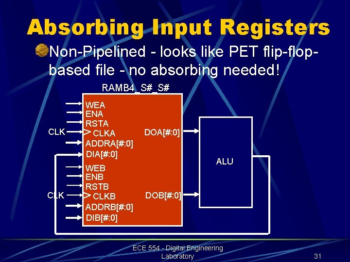
Absorbing Input Registers Non-Pipelined - looks like PET flip-flopbased file - no absorbing needed! RAMB 4_S#_S# CLK WEA ENA RSTA CLKA ADDRA[#: 0] DIA[#: 0] DOA[#: 0] WEB ENB RSTB CLKB ADDRB[#: 0] DIB[#: 0] DOB[#: 0] ALU ECE 554 - Digital Engineering Laboratory 31

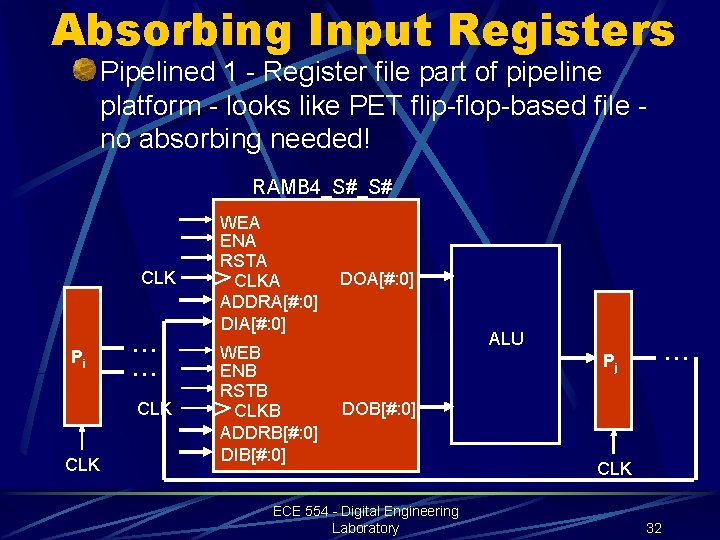
Absorbing Input Registers Pipelined 1 - Register file part of pipeline platform - looks like PET flip-flop-based file no absorbing needed! RAMB 4_S#_S# CLK Pi . . . CLK WEA ENA RSTA CLKA ADDRA[#: 0] DIA[#: 0] WEB ENB RSTB CLKB ADDRB[#: 0] DIB[#: 0] DOA[#: 0] ALU . . . Pj DOB[#: 0] ECE 554 - Digital Engineering Laboratory CLK 32

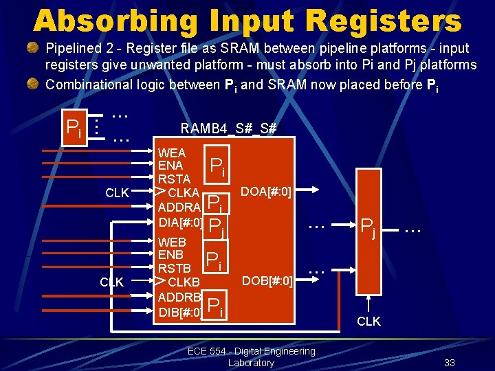
Absorbing Input Registers Pipelined 2 - Register file as SRAM between pipeline platforms - input registers give unwanted platform - must absorb into Pi and Pj platforms Combinational logic between Pi and SRAM now placed before Pi . . . CLK RAMB 4_S#_S# WEA ENA Pi RSTA CLKA Pi ADDRA[#: 0] DIA[#: 0] P j WEB ENB Pi RSTB CLKB ADDRB[#: 0] DIB[#: 0] Pi DOA[#: 0] . . . DOB[#: 0] Pj . . . ECE 554 - Digital Engineering Laboratory CLK 33

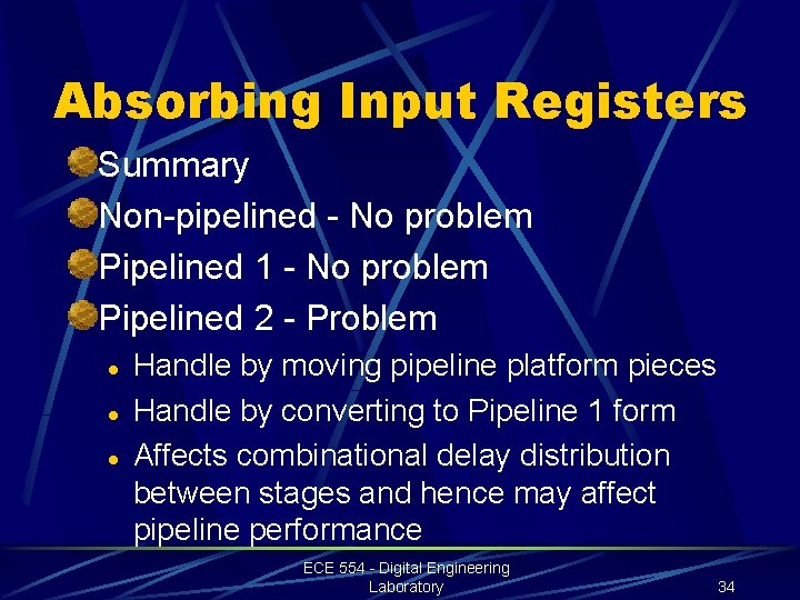
Absorbing Input Registers Summary Non-pipelined - No problem Pipelined 1 - No problem Pipelined 2 - Problem l l l Handle by moving pipeline platform pieces Handle by converting to Pipeline 1 form Affects combinational delay distribution between stages and hence may affect pipeline performance ECE 554 - Digital Engineering Laboratory 34

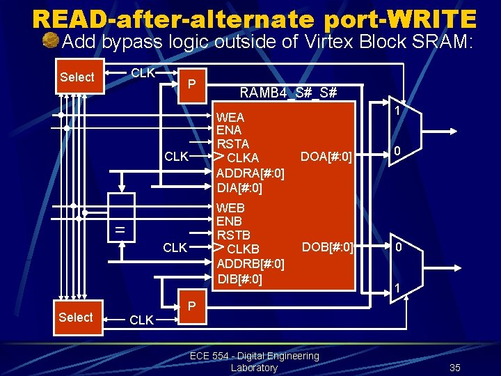
READ-after-alternate port-WRITE Add bypass logic outside of Virtex Block SRAM: CLK Select P CLK 1 CLK WEA ENA RSTA CLKA ADDRA[#: 0] DIA[#: 0] DOA[#: 0] 0 CLK WEB ENB RSTB CLKB ADDRB[#: 0] DIB[#: 0] DOB[#: 0] 0 = Select RAMB 4_S#_S# 1 P ECE 554 - Digital Engineering Laboratory 35

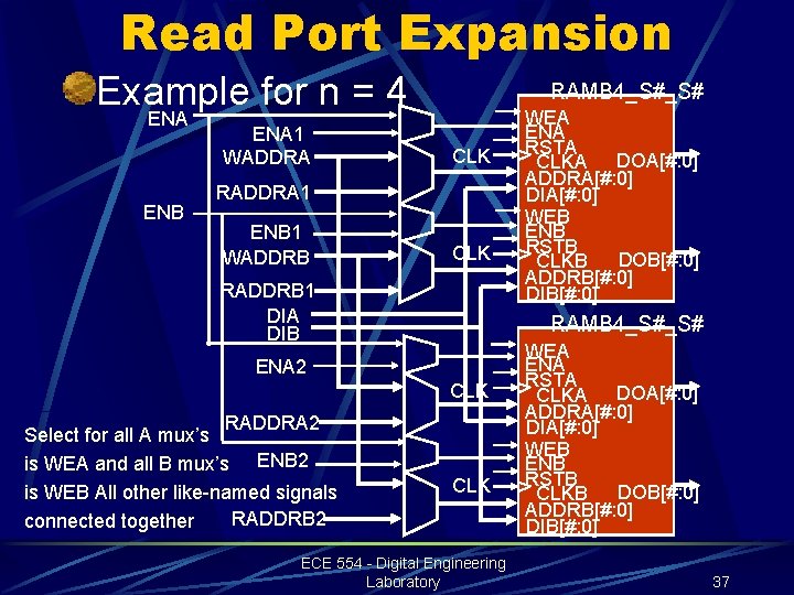
Read Port Expansion to n R address/data ports l Place ceiling(n/2) SRAMs in parallel with the two writes accomplished by: l l Applying same address to all ADDRA and the same address to all ADDRB, and Wiring together all DIA ports and all DIB ports ECE 554 - Digital Engineering Laboratory 36

Read Port Expansion Example for n = 4 ENA ENB ENA 1 WADDRA RAMB 4_S#_S# CLK RADDRA 1 ENB 1 WADDRB CLK RADDRB 1 DIA DIB RAMB 4_S#_S# ENA 2 CLK RADDRA 2 Select for all A mux’s is WEA and all B mux’s ENB 2 is WEB All other like-named signals RADDRB 2 connected together WEA ENA RSTA CLKA DOA[#: 0] ADDRA[#: 0] DIA[#: 0] WEB ENB RSTB DOB[#: 0] CLKB ADDRB[#: 0] DIB[#: 0] CLK ECE 554 - Digital Engineering Laboratory WEA ENA RSTA CLKA DOA[#: 0] ADDRA[#: 0] DIA[#: 0] WEB ENB RSTB DOB[#: 0] CLKB ADDRB[#: 0] DIB[#: 0] 37

Inter-operation Address Dependency READ-after-WRITE - Can be done for one WRITE two READs with two parallel Dual Port Block SRAMs with READ-after-alternate port-WRITE logic added to READ side of both. l l Parallel WRITE on A ports Independent parallel READs on B-ports Each additional parallel Dual Port Block SRAM adds one more READ port Cannot accomplish WRITE-after-READ Cannot be done for more than one active WRITE port without using WRITE Port Expansion ECE 554 - Digital Engineering Laboratory 38

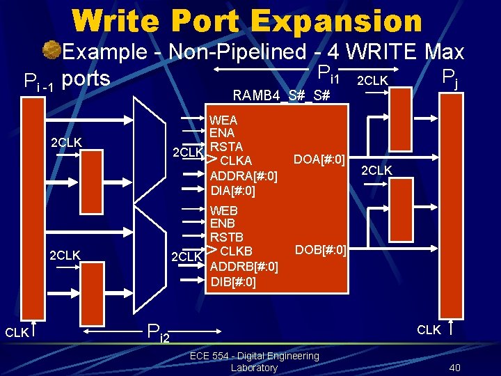
Write Port Expansion Requires “super-clocking, ” in which a clock having a multiple of the frequency of the fundamental operational clock is used to serialize Block SRAM operations. Requires additional registers to locally enter into and return from serialized operations Muxes required that are switched by the a flip-flop driven by the faster clock ECE 554 - Digital Engineering Laboratory 39

Write Port Expansion Pi -1 Example - Non-Pipelined - 4 WRITE Max Pi 1 2 CLK Pj ports RAMB 4_S#_S# 2 CLK CLK WEA ENA 2 CLK RSTA CLKA ADDRA[#: 0] DIA[#: 0] DOA[#: 0] WEB ENB RSTB 2 CLK CLKB ADDRB[#: 0] DIB[#: 0] DOB[#: 0] Pi 2 2 CLK ECE 554 - Digital Engineering Laboratory 40

Absorbing Output Latches The output latch is a part of the attempt at a “flip-flop” appearance for the SRAM operation. As such, there appears to be no way to explicitly work around it Other workarounds handle its effects ECE 554 - Digital Engineering Laboratory 41

The Bottom Line Overall, it appears that the best approach is to: l l l Use a Non-Pipelined or Pipeline 1 structure Use the Interoperation Dependency solution to achieve multiple dependency-free READs Use WRITE Port Expansion for multiple WRITEs Use the READ-after-alternate port-WRITE to get READafter-WRITE capability Use WRITE Port Expansion with READs on early subcycles to get WRITE-after-READ capability Be cognizant of substantial setup times and delays for the synchronous operations Feel free to experiment with other approaches and apply ideas given to other Virtex Block SRAM uses ECE 554 - Digital Engineering Laboratory 42

Memories Timing Issues Width Expansion ECE 554 - Digital Engineering Laboratory 43

Timing Issues The off-board SRAMs are asynchronous and have typical signal timing requirements See AS 7 C 4096 Datasheets for timing parameters l l Address controlled READ is easy WE-controlled WRITE has zero setup and hold times which look easy, but read on Due to unpredictable FPGA timing, timing of memory signals, particularly for WRITE should be verified. In worst case, may need to use “super clocking” to get reliable timing ECE 554 - Digital Engineering Laboratory 44

Width Expansion Width expansion can be achieved by using “super clocking” with implementation similar to that for register file write expansion. To expand a 16 -bit word to a 16 n bit word requires “super clocking” at n times the fundamental rate. ECE 554 - Digital Engineering Laboratory 45

Width Expansion Implementation l l For address-controlled READs, straightforward Not recommended, although feasible, for WRITEs: l l Must be trailing edges on, for example, WE, for each of the super clock cycles This will require changes on negative as well as positive super clock edges ECE 554 - Digital Engineering Laboratory 46

Postscript The workarounds do not consider: l l Multiple clock edge use instead of superclocking Different clock edges on the two ports on a dual port Select. RAM These techniques can potentially be beneficial to the degree that: l l the resulting constructs are synthesizable, and do not adversely affect performance ECE 554 - Digital Engineering Laboratory 47