Recent Activities on HVCMOS Detectors at KIT Ivan

- Slides: 23

Recent Activities on HV-CMOS Detectors at KIT Ivan Peric KIT – Universität des Landes Baden-Württemberg und nationales Forschungszentrum in der Helmholtz-Gemeinschaft www. kit. edu

Introduction of HVCMOS Engineering run in a. H 18 process, experimental results New foundry: TSI ATLASPIX 3 Planned new engineering run CLIC designs New ideas: small pixels and reduced detector capacitance 2 CLIC DP collaboration meeting, August 2019

Introduction HVCMOS sensors, for CLIC, Mu 3 e, ATLAS, COMPASS, LHCB, P 2, Belle II (planned) Motivation For ATLAS HVCMOS sensors promise large cost saving (> 10 M), simpler module production, better reliability, less material… For Mu 3 e HVMOS is practically the only option since a high time resolution is needed and material budget is low (0. 1% of radiation length/layer - sensor must be 50µm thin) HVCMOS = depleted CMOS sensors with large collecting n-well electrode and pixel electronics inside 3 CLIC DP collaboration meeting, August 2019

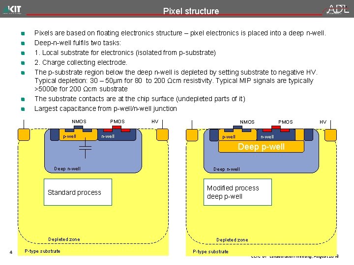
Pixel structure Pixels are based on floating electronics structure – pixel electronics is placed into a deep n-well. Deep-n-well fulfils two tasks: 1. Local substrate for electronics (isolated from p-substrate) 2. Charge collecting electrode. The p-substrate region below the deep n-well is depleted by setting substrate to negative HV. Typical depletion: 30 – 50µm for 80 to 200 Ωcm resistivity. Typical MIP signals are typically >5000 e for 200 Ωcm substrate The substrate contacts are at the chip surface (undepleted parts of it) Largest capacitance from p-well/n-well junction NMOS p-well PMOS n-well HV NMOS p-well PMOS HV n-well Deep p-well Deep n-well Standard process Depleted zone 4 P-type substrate Deep n-well Modified process deep p-well Depleted zone P-type substrate CLIC DP collaboration meeting, August 2019

AMSH 18 run The milestone in our development was the combined Mu 3 e and ATLAS run done in AMS a. H 18 process This process is compatible with the originally developed H 18 (CMHV 7 SF) process from IBM (now Global Foundries) For this engineering run, AMS modified the process in two aspects – high resistivity substrates were used and the deep-well layer added to isolate the deep n-well from shallow n-well. Not all designs used this option 5 CLIC DP collaboration meeting, August 2019

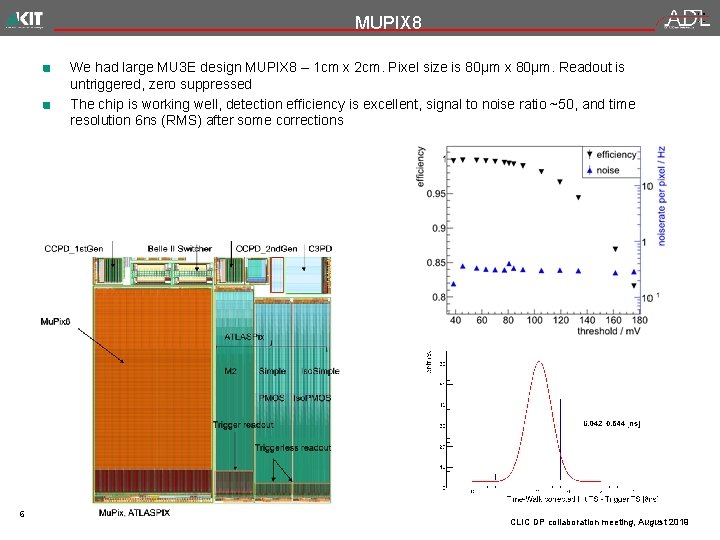
MUPIX 8 We had large MU 3 E design MUPIX 8 – 1 cm x 2 cm. Pixel size is 80µm x 80µm. Readout is untriggered, zero suppressed The chip is working well, detection efficiency is excellent, signal to noise ratio ~50, and time resolution 6 ns (RMS) after some corrections 6 CLIC DP collaboration meeting, August 2019

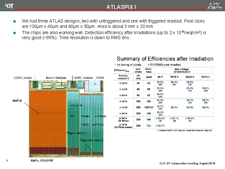
ATLASPIX 1 We had three ATLAS designs, two with untriggered and one with triggered readout. Pixel sizes are 130µm x 40µm and 60µm x 50µm. Area is about 3 mm x 20 mm The chips are also working well. Detection efficiency after irradiations (up to 2 x 10¹⁵ neq/cm 2) is very good (~99%). Time resolution is down to RMS 8 ns. 7 CLIC DP collaboration meeting, August 2019

Deep p-well was used in one of the ATLASPIX simple chips to isolate CMOS comparator from sensor electrode. Another twin chips used no isolation and used NMOS-based comparator. Both versions of comparator worked good The use of deep p-well simplifies the comparator design and allows full swing output which makes the design more robust 8 CLIC DP collaboration meeting, August 2019

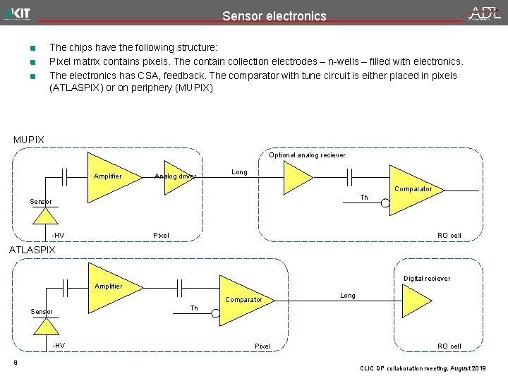
Sensor electronics The chips have the following structure: Pixel matrix contains pixels. The contain collection electrodes – n-wells – filled with electronics. The electronics has CSA, feedback. The comparator with tune circuit is either placed in pixels (ATLASPIX) or on periphery (MUPIX) MUPIX Optional analog reciever Amplifier Analog driver Long Comparator Th Sensor -HV Pixel RO cell ATLASPIX Digital reciever Amplifier Comparator Th Sensor -HV 9 Long Pixel RO cell CLIC DP collaboration meeting, August 2019

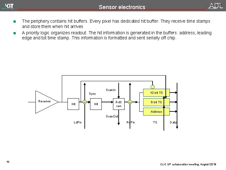
Sensor electronics The periphery contains hit buffers. Every pixel has dedicated hit buffer. They receive time stamps and store them when hit arrives A priority logic organizes readout. The hit information is generated in the buffers: address, leading edge and tot time stamp. This information is formatted and sent serially off chip. Scan. In 10 bit TS Sync Receiver Hit x Hit Rd. S can x 6 bit TS Address Scan. Out Ld. Pix 10 Rd. Pix TS Data CLIC DP collaboration meeting, August 2019

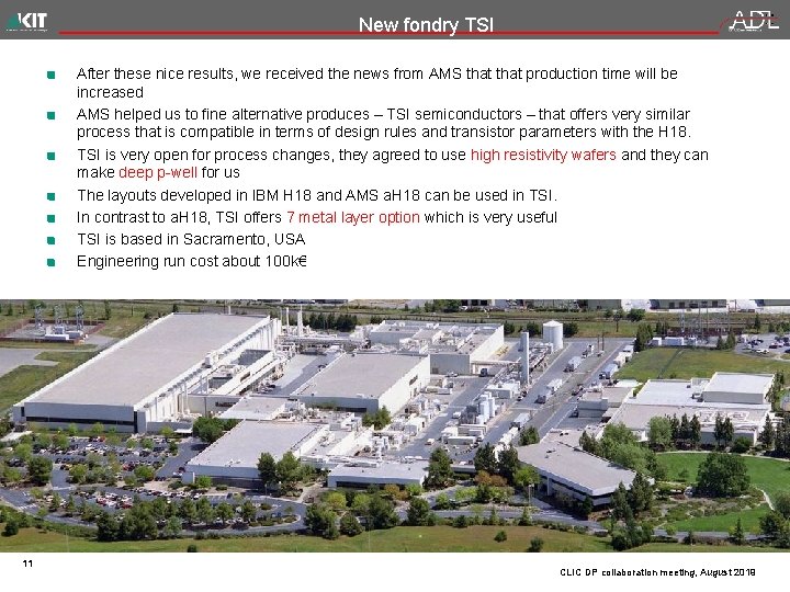
New fondry TSI After these nice results, we received the news from AMS that production time will be increased AMS helped us to fine alternative produces – TSI semiconductors – that offers very similar process that is compatible in terms of design rules and transistor parameters with the H 18. TSI is very open for process changes, they agreed to use high resistivity wafers and they can make deep p-well for us The layouts developed in IBM H 18 and AMS a. H 18 can be used in TSI. In contrast to a. H 18, TSI offers 7 metal layer option which is very useful TSI is based in Sacramento, USA Engineering run cost about 100 k€ 11 CLIC DP collaboration meeting, August 2019

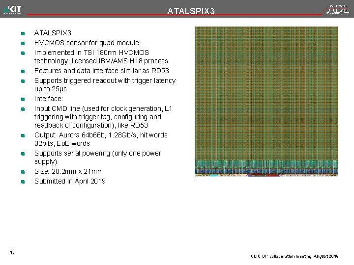
ATLASPIX 3 chip designed in TSI process. This is a large chip 2 x 2 cm chip with 50µm x 150µm pixels. It has the same signal interface as Rd 53 and it can be used to build quad modules for ATLAS It has implemented triggered- and, as test feature, untriggered readout 12 CLIC DP collaboration meeting, August 2019

ATALSPIX 3 HVCMOS sensor for quad module Implemented in TSI 180 nm HVCMOS technology, licensed IBM/AMS H 18 process Features and data interface similar as RD 53 Supports triggered readout with trigger latency up to 25µs Interface: Input CMD line (used for clock generation, L 1 triggering with trigger tag, configuring and readback of configuration), like RD 53 Output: Aurora 64 b 66 b, 1. 28 Gb/s, hit words 32 bits, Eo. E words Supports serial powering (only one power supply) Size: 20. 2 mm x 21 mm Submitted in April 2019 13 CLIC DP collaboration meeting, August 2019

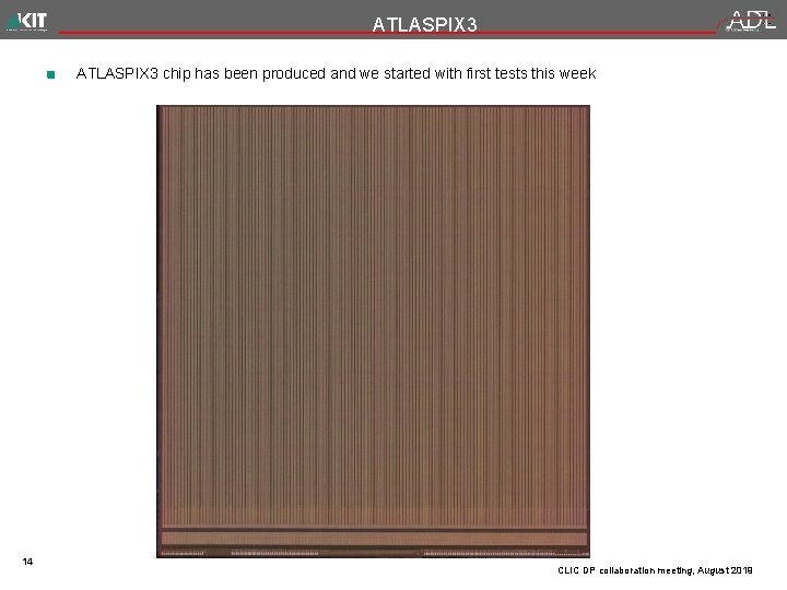
ATLASPIX 3 chip has been produced and we started with first tests this week 14 CLIC DP collaboration meeting, August 2019

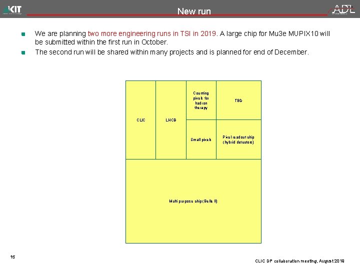
New run We are planning two more engineering runs in TSI in 2019. A large chip for Mu 3 e MUPIX 10 will be submitted within the first run in October. The second run will be shared within many projects and is planned for end of December. CLIC Counting pixels for hadron therapy TBD Small pixels Pixel readout chip (hybrid detectors) LHCB Multi purpose chip (Belle II) 15 CLIC DP collaboration meeting, August 2019

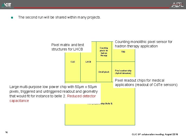
The second run will be shared within many projects. Pixel matrix and test structures for LHCB CLIC Counting pixels for hadron therapy Counting monolithic pixel sensor for hadron therapy application TBD LHCB Small pixels Large multi-purpose low power chip with 50µm x 50µm pixels, triggered and untriggered readout and geometry that would fit for instance to belle 2. Reduced detector capacitance Pixel readout chip (hybrid detectors) Pixel readout chips for medical applications (readout of Cd. Te sensors) Multi purpose chip (Belle II) 16 CLIC DP collaboration meeting, August 2019

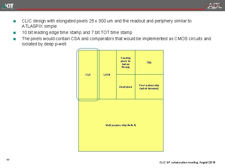
CLIC design with elongated pixels 25 x 300 um and the readout and periphery similar to ATLASPIX simple 10 bit leading edge time stamp and 7 bit TOT time stamp The pixels would contain CSA and comparators that would be implemented as CMOS circuits and isolated by deep p-well. CLIC Counting pixels for hadron therapy TBD Small pixels Pixel readout chip (hybrid detectors) LHCB Multi purpose chip (Belle II) 17 CLIC DP collaboration meeting, August 2019

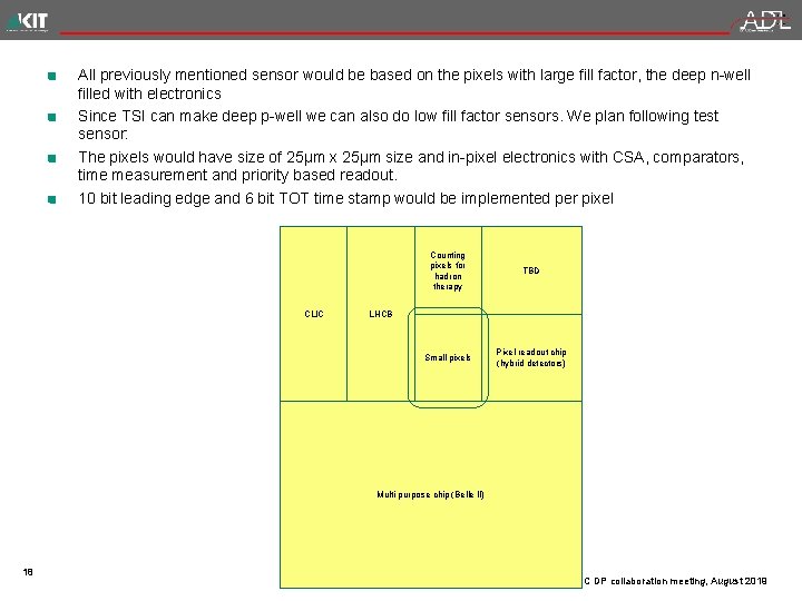
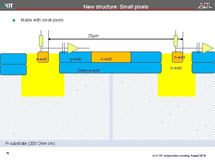
All previously mentioned sensor would be based on the pixels with large fill factor, the deep n-well filled with electronics Since TSI can make deep p-well we can also do low fill factor sensors. We plan following test sensor: The pixels would have size of 25µm x 25µm size and in-pixel electronics with CSA, comparators, time measurement and priority based readout. 10 bit leading edge and 6 bit TOT time stamp would be implemented per pixel CLIC Counting pixels for hadron therapy TBD Small pixels Pixel readout chip (hybrid detectors) LHCB Multi purpose chip (Belle II) 18 CLIC DP collaboration meeting, August 2019

New structure: Small pixels Matrix with small pixels 25µm n-well p-well Deep p-well n-well P-substrate (200 Ohm cm) 19 CLIC DP collaboration meeting, August 2019

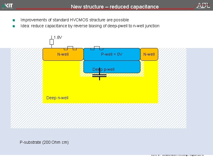
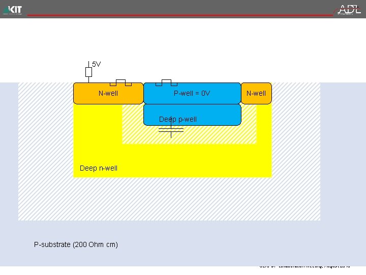
New structure – reduced capacitance Improvements of standard HVCMOS stracture are possible Idea: reduce capacitance by reverse biasing of deep-pwell to n-well junction 1. 8 V N-well P-well = 0 V N-well Deep p-well Deep n-well P-substrate (200 Ohm cm) 20 CLIC DP collaboration meeting, August 2019

5 V N-well P-well = 0 V N-well Deep p-well Deep n-well P-substrate (200 Ohm cm) 21 CLIC DP collaboration meeting, August 2019

Summary Engineering run in a. H 18 process, experimental results presented New foundry: TSI ATLASPIX 3 introduced Planned new engineering run CLIC designs New ideas: small monolithic pixels and reduced detector capacitance 22 CLIC DP collaboration meeting, August 2019

Thank you 23 CLIC DP collaboration meeting, August 2019