HVCMOS Overview Ivan Peric Felix Ehrler Rudolf Schimassek


- Slides: 60

HVCMOS - Overview Ivan Peric, Felix Ehrler, Rudolf Schimassek on behalf of HVCMOS collaboration KIT – Universität des Landes Baden-Württemberg und nationales Forschungszentrum in der Helmholtz-Gemeinschaft www. kit. edu

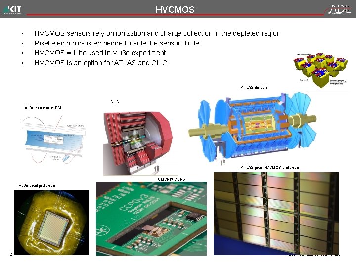
HVCMOS • • HVCMOS sensors rely on ionization and charge collection in the depleted region Pixel electronics is embedded inside the sensor diode HVCMOS will be used in Mu 3 e experiment HVCMOS is an option for ATLAS and CLIC ATLAS detector CLIC Mu 3 e detector at PSI ATLAS pixel HVCMOS prototype CLICPIX CCPD Mu 3 e-pixel prototype 2 AIDA Simulation Workshop

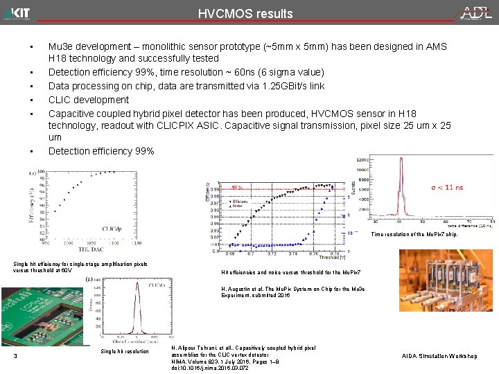
HVCMOS results • • • Mu 3 e development – monolithic sensor prototype (~5 mm x 5 mm) has been designed in AMS H 18 technology and successfully tested Detection efficiency 99%, time resolution ~ 60 ns (6 sigma value) Data processing on chip, data are transmitted via 1. 25 GBit/s link CLIC development Capacitive coupled hybrid pixel detector has been produced, HVCMOS sensor in H 18 technology, readout with CLICPIX ASIC. Capacitive signal transmission, pixel size 25 um x 25 um Detection efficiency 99% Time resolution of the Mu. Pix 7 chip. Single hit efficiency for single-stage amplification pixels versus threshold at 60 V Hit effciencies and noise versus threshold for the Mu. Pix 7 H. Augustin et al. The Mu. Pix System-on-Chip for the Mu 3 e Experiment, submitted 2016 3 Single hit resolution N. Alipour Tehrani, et all. , Capacitively coupled hybrid pixel assemblies for the CLIC vertex detector NIMA, Volume 823, 1 July 2016, Pages 1– 8 doi: 10. 1016/j. nima. 2016. 03. 072 AIDA Simulation Workshop

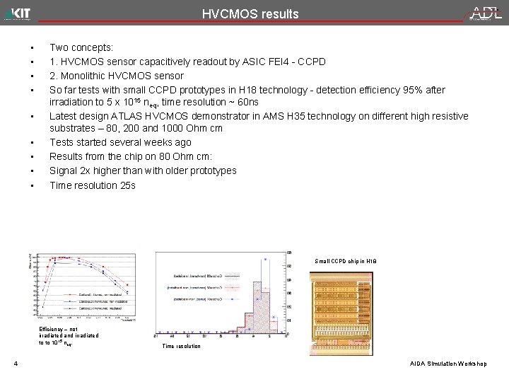
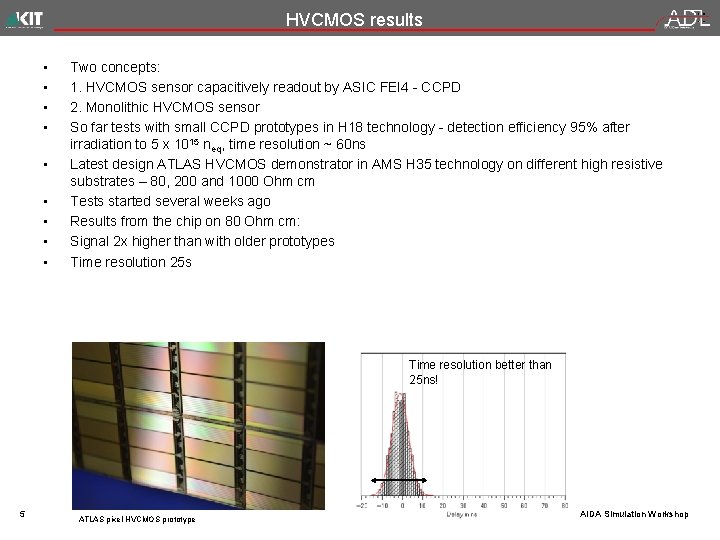
HVCMOS results • • • Two concepts: 1. HVCMOS sensor capacitively readout by ASIC FEI 4 - CCPD 2. Monolithic HVCMOS sensor So far tests with small CCPD prototypes in H 18 technology - detection efficiency 95% after irradiation to 5 x 10¹⁵ neq, time resolution ~ 60 ns Latest design ATLAS HVCMOS demonstrator in AMS H 35 technology on different high resistive substrates – 80, 200 and 1000 Ohm cm Tests started several weeks ago Results from the chip on 80 Ohm cm: Signal 2 x higher than with older prototypes Time resolution 25 s Small CCPD chip in H 18 Efficiency – not irradiated and irradiated to to 1015 neq, 4 Time resolution AIDA Simulation Workshop

HVCMOS results • • • Two concepts: 1. HVCMOS sensor capacitively readout by ASIC FEI 4 - CCPD 2. Monolithic HVCMOS sensor So far tests with small CCPD prototypes in H 18 technology - detection efficiency 95% after irradiation to 5 x 10¹⁵ neq, time resolution ~ 60 ns Latest design ATLAS HVCMOS demonstrator in AMS H 35 technology on different high resistive substrates – 80, 200 and 1000 Ohm cm Tests started several weeks ago Results from the chip on 80 Ohm cm: Signal 2 x higher than with older prototypes Time resolution 25 s Time resolution better than 25 ns! 5 ATLAS pixel HVCMOS prototype AIDA Simulation Workshop

H 35 DEMO Large HVCMOS Detector on High Resistive Substrate in AMS Technology Ivan Peric KIT – Universität des Landes Baden-Württemberg und nationales Forschungszentrum in der Helmholtz-Gemeinschaft www. kit. edu

H 35 DEMO chip • • • 7 The first reticle size HV-CMOS demonstrator for ATLAS pixel layers has been produced as full mask run – producer AMS H 35 HVCMOS technology (350 nm) The design of the sensor and financing of its production have been done in collaboration between University of Bern, IFAE Barcelona, CERN, University of Geneva, University of Liverpool and KIT AIDA Simulation Workshop

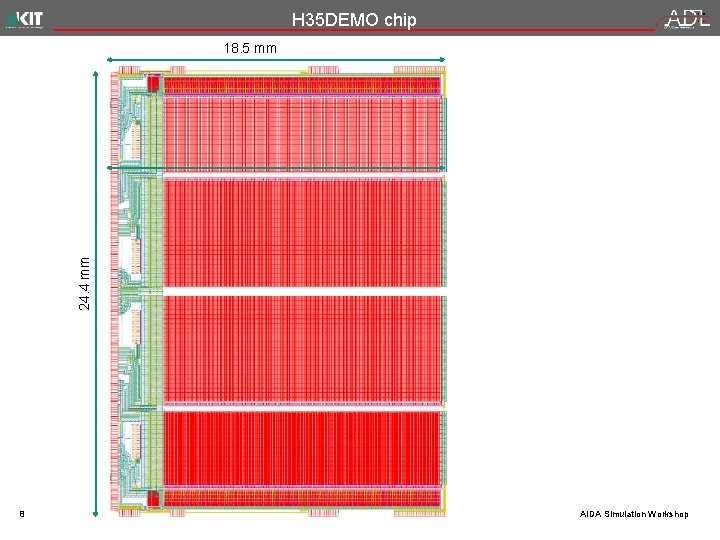
H 35 DEMO chip 24. 4 mm 18. 5 mm 8 AIDA Simulation Workshop

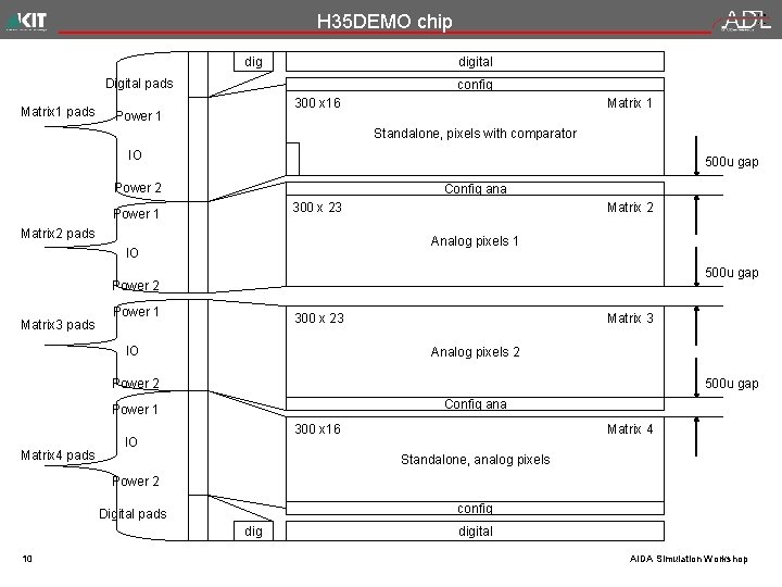
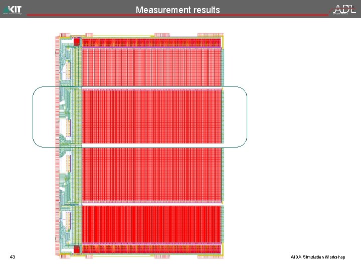
The chips contain four pixel matrices which are independent and have separated pads 9 AIDA Simulation Workshop

H 35 DEMO chip digital Digital pads Matrix 1 pads config 300 x 16 Power 1 Matrix 1 Standalone, pixels with comparator IO 500 u gap Power 2 Config ana 300 x 23 Power 1 Matrix 2 pads Matrix 2 Analog pixels 1 IO 500 u gap Power 2 Matrix 3 pads Power 1 300 x 23 IO Matrix 3 Analog pixels 2 Power 2 500 u gap Config ana Power 1 Matrix 4 pads 300 x 16 IO Matrix 4 Standalone, analog pixels Power 2 config Digital pads dig 10 digital AIDA Simulation Workshop

H 35 DEMO chip The sensors have been produced on p-type substrates with four different substrate resistivities: 20, 80 (50 -100), 200 (200 -400) and 1000 (600 -2000) Ωcm 11 AIDA Simulation Workshop

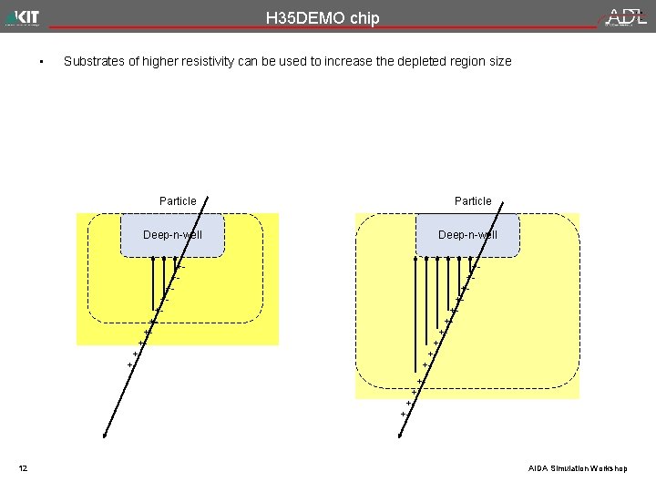
H 35 DEMO chip • Substrates of higher resistivity can be used to increase the depleted region size Particle Deep-n-well +++++- 12 Particle Deep-n-well +++++++- AIDA Simulation Workshop

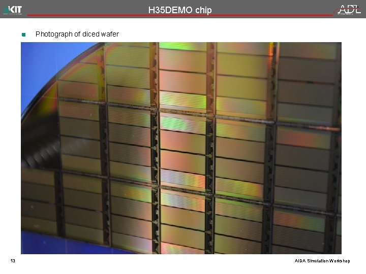
H 35 DEMO chip Photograph of diced wafer 13 AIDA Simulation Workshop

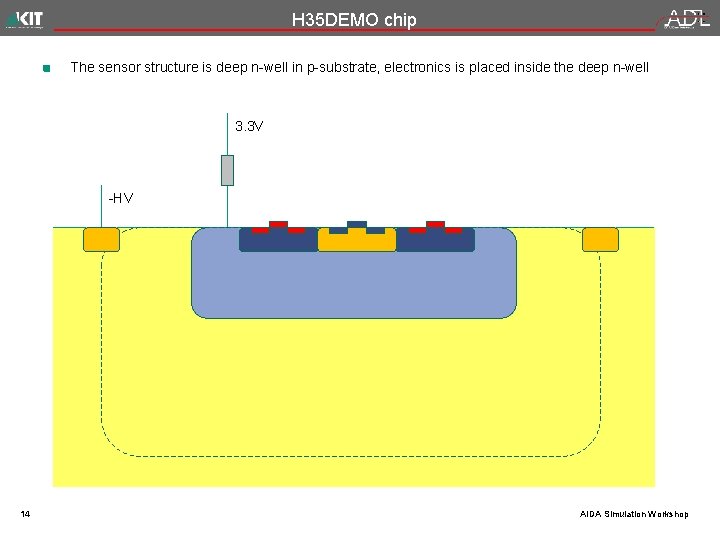
H 35 DEMO chip The sensor structure is deep n-well in p-substrate, electronics is placed inside the deep n-well 3. 3 V -HV 14 AIDA Simulation Workshop

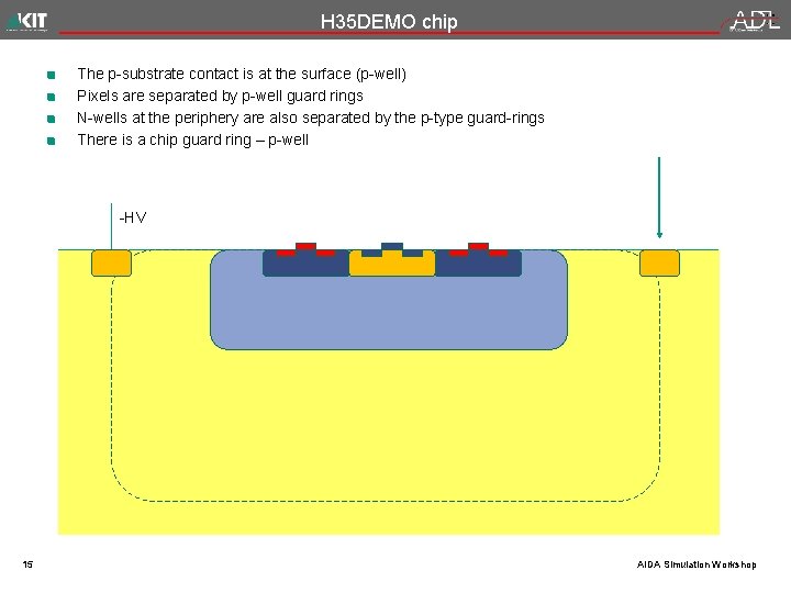
H 35 DEMO chip The p-substrate contact is at the surface (p-well) Pixels are separated by p-well guard rings N-wells at the periphery are also separated by the p-type guard-rings There is a chip guard ring – p-well -HV 15 AIDA Simulation Workshop

H 35 DEMO chip Post processing of wafers is planned Thinning and backside contact Bump bonding TSV 16 AIDA Simulation Workshop

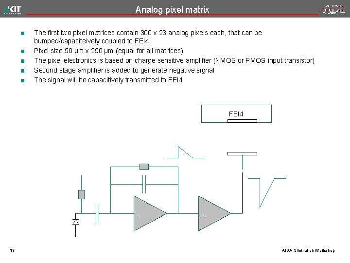
Analog pixel matrix The first two pixel matrices contain 300 x 23 analog pixels each, that can be bumped/capaciteively coupled to FEI 4 Pixel size 50 µm x 250 µm (equal for all matrices) The pixel electronics is based on charge sensitive amplifier (NMOS or PMOS input transistor) Second stage amplifier is added to generate negative signal The signal will be capacitively transmitted to FEI 4 - 17 - AIDA Simulation Workshop

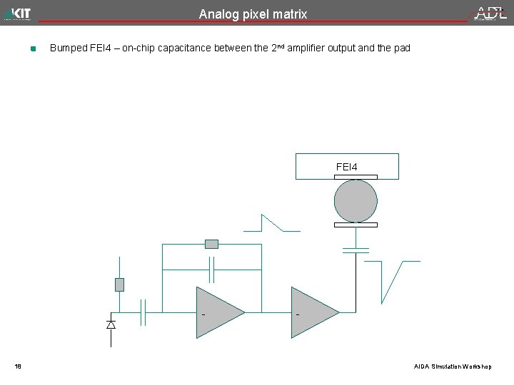
Analog pixel matrix Bumped FEI 4 – on-chip capacitance between the 2 nd amplifier output and the pad FEI 4 - 18 - AIDA Simulation Workshop

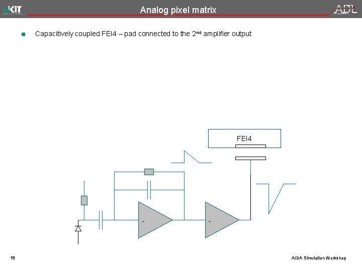
Analog pixel matrix Capacitively coupled FEI 4 – pad connected to the 2 nd amplifier output FEI 4 - 19 - AIDA Simulation Workshop

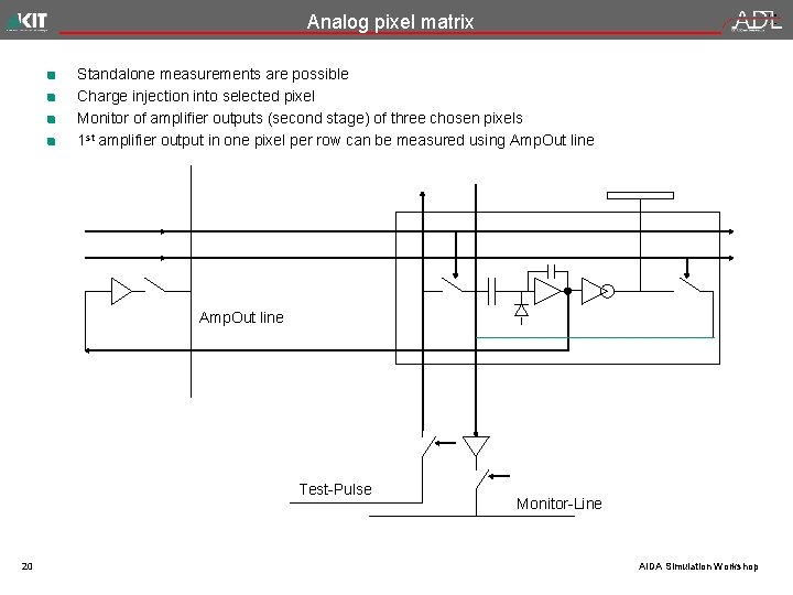
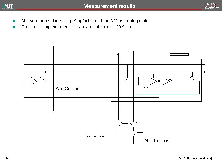
Analog pixel matrix Standalone measurements are possible Charge injection into selected pixel Monitor of amplifier outputs (second stage) of three chosen pixels 1 st amplifier output in one pixel per row can be measured using Amp. Out line Test-Pulse 20 Monitor-Line AIDA Simulation Workshop

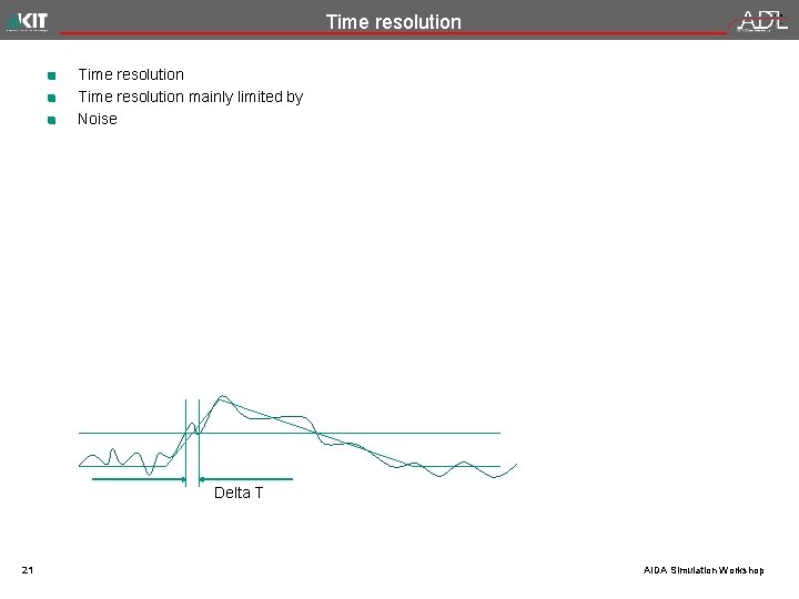
Time resolution mainly limited by Noise Delta T 21 AIDA Simulation Workshop

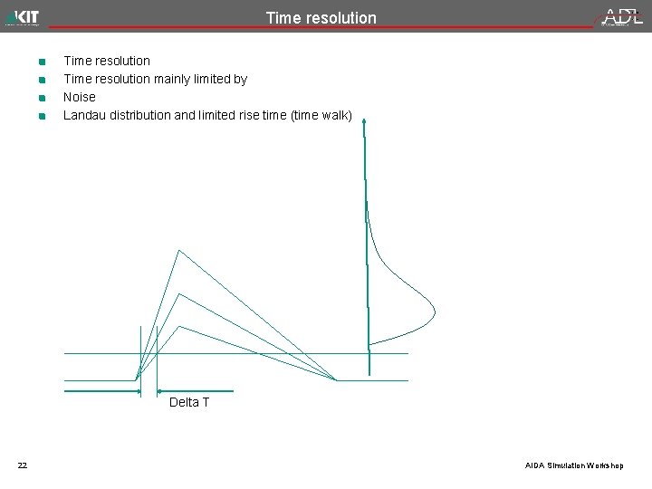
Time resolution mainly limited by Noise Landau distribution and limited rise time (time walk) Delta T 22 AIDA Simulation Workshop

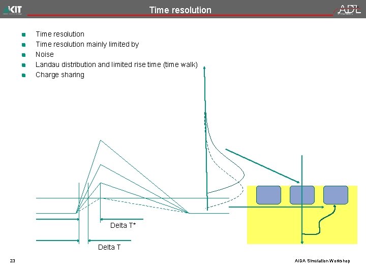
Time resolution mainly limited by Noise Landau distribution and limited rise time (time walk) Charge sharing Delta T* Delta T 23 AIDA Simulation Workshop

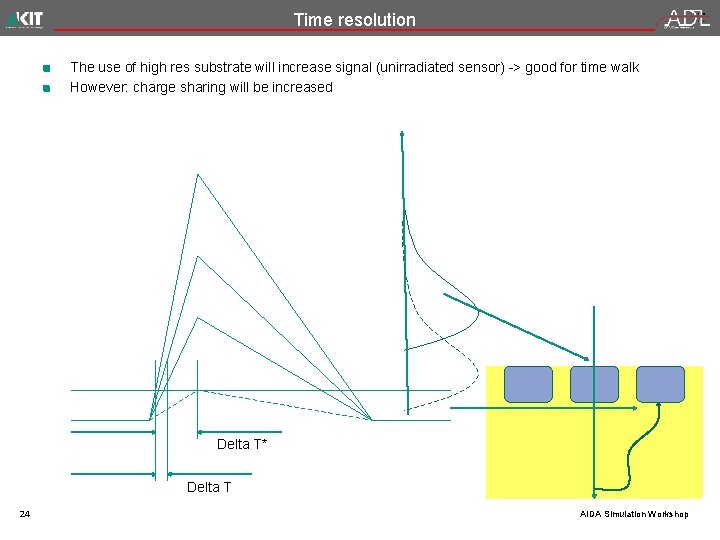
Time resolution The use of high res substrate will increase signal (unirradiated sensor) -> good for time walk However: charge sharing will be increased Delta T* Delta T 24 AIDA Simulation Workshop

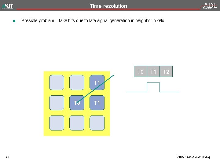
Time resolution Possible problem – fake hits due to late signal generation in neighbor pixels T 0 T 1 T 2 T 1 T 0 25 T 1 AIDA Simulation Workshop

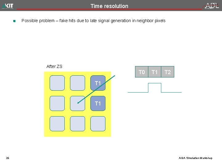
Time resolution Possible problem – fake hits due to late signal generation in neighbor pixels After ZS T 0 T 1 T 2 T 1 26 AIDA Simulation Workshop

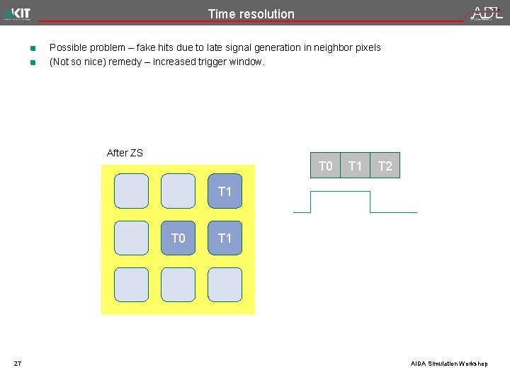
Time resolution Possible problem – fake hits due to late signal generation in neighbor pixels (Not so nice) remedy – increased trigger window. After ZS T 0 T 1 T 2 T 1 T 0 27 T 1 AIDA Simulation Workshop

Time resolution Additional problem: signal amplitude after irradiation is unknown => We tried to improve time resolution for standard (low res signals) by designing clever electronics 28 AIDA Simulation Workshop

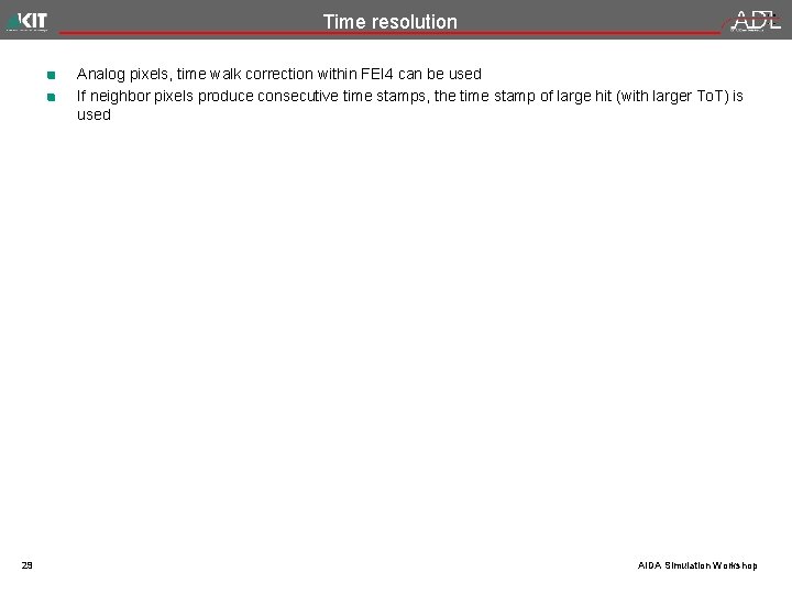
Time resolution Analog pixels, time walk correction within FEI 4 can be used If neighbor pixels produce consecutive time stamps, the time stamp of large hit (with larger To. T) is used 29 AIDA Simulation Workshop

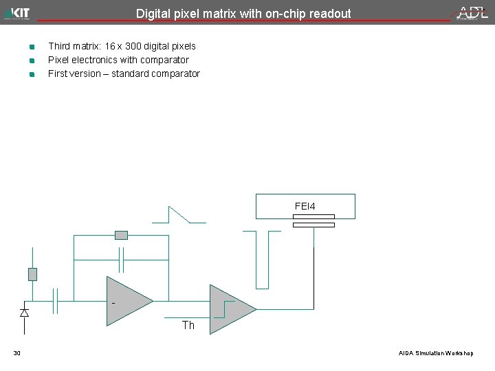
Digital pixel matrix with on-chip readout Third matrix: 16 x 300 digital pixels Pixel electronics with comparator First version – standard comparator FEI 4 Th 30 AIDA Simulation Workshop

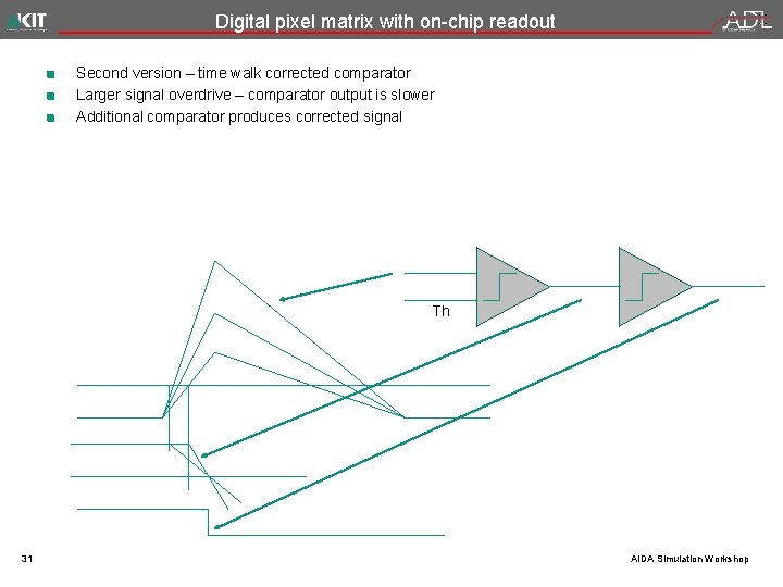
Digital pixel matrix with on-chip readout Second version – time walk corrected comparator Larger signal overdrive – comparator output is slower Additional comparator produces corrected signal Th 31 AIDA Simulation Workshop

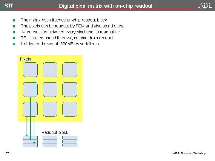
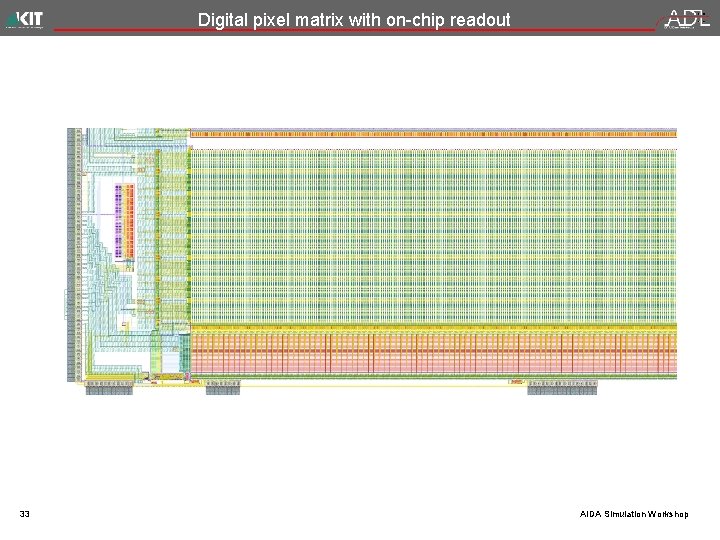
Digital pixel matrix with on-chip readout The matrix has attached on-chip readout block The pixels can be readout by FEI 4 and also stand alone 1 -1 connection between every pixel and its readout cell TS is stored upon hit arrival, column drain readout Untriggered readout, 320 MBit/s serializers Pixels Readout block 32 AIDA Simulation Workshop

Digital pixel matrix with on-chip readout 33 AIDA Simulation Workshop

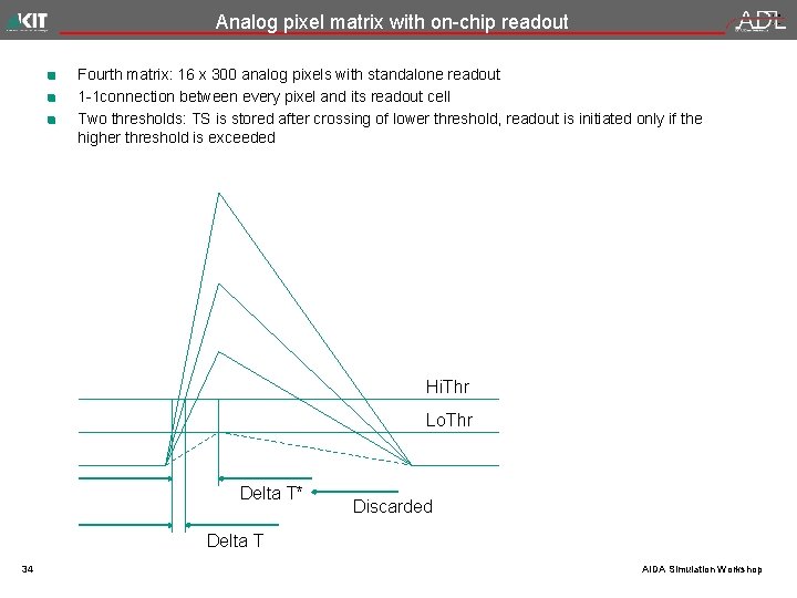
Analog pixel matrix with on-chip readout Fourth matrix: 16 x 300 analog pixels with standalone readout 1 -1 connection between every pixel and its readout cell Two thresholds: TS is stored after crossing of lower threshold, readout is initiated only if the higher threshold is exceeded Hi. Thr Lo. Thr Delta T* Discarded Delta T 34 AIDA Simulation Workshop

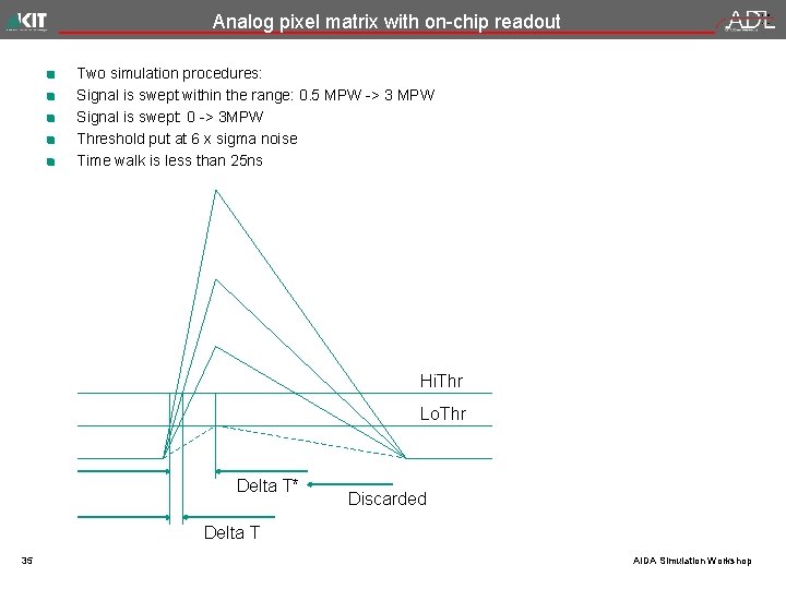
Analog pixel matrix with on-chip readout Two simulation procedures: Signal is swept within the range: 0. 5 MPW -> 3 MPW Signal is swept: 0 -> 3 MPW Threshold put at 6 x sigma noise Time walk is less than 25 ns Hi. Thr Lo. Thr Delta T* Discarded Delta T 35 AIDA Simulation Workshop

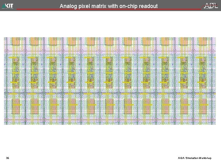
Analog pixel matrix with on-chip readout 36 AIDA Simulation Workshop

Test structures Several test structures 37 AIDA Simulation Workshop

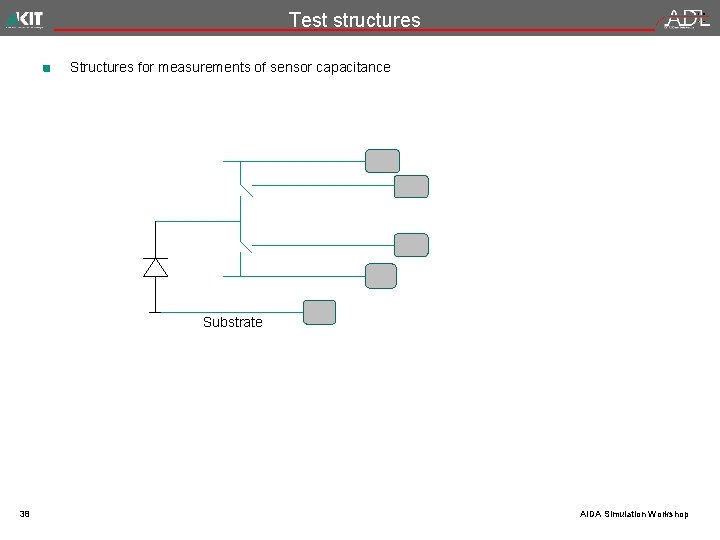
Test structures Structures for measurements of sensor capacitance Substrate 38 AIDA Simulation Workshop

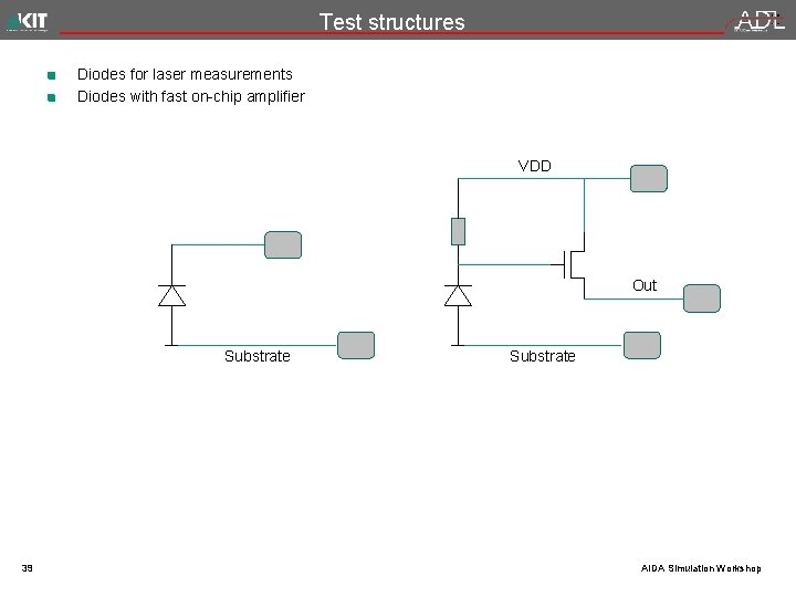
Test structures Diodes for laser measurements Diodes with fast on-chip amplifier VDD Out Substrate 39 Substrate AIDA Simulation Workshop

Measurement Results Ivan Peric KIT – Universität des Landes Baden-Württemberg und nationales Forschungszentrum in der Helmholtz-Gemeinschaft www. kit. edu

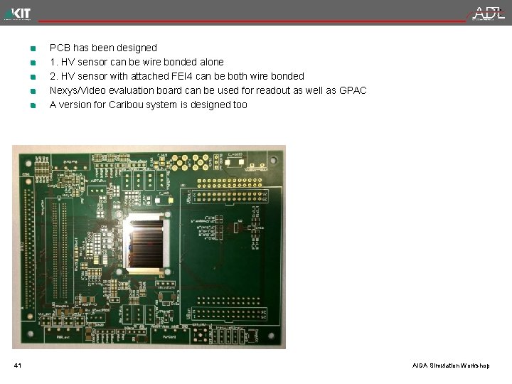
PCB has been designed 1. HV sensor can be wire bonded alone 2. HV sensor with attached FEI 4 can be both wire bonded Nexys/Video evaluation board can be used for readout as well as GPAC A version for Caribou system is designed too 41 AIDA Simulation Workshop

Measurement results Measurements done using Amp. Out line of the NMOS analog matrix The chip is implemented on standard substrate – 20 Ω cm Amp. Out line Test-Pulse 42 Monitor-Line AIDA Simulation Workshop

Measurement results 43 AIDA Simulation Workshop

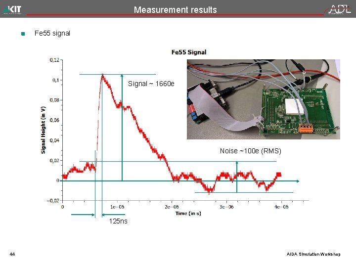
Measurement results Fe 55 signal Signal ~ 1660 e Noise ~100 e (RMS) 125 ns 44 AIDA Simulation Workshop

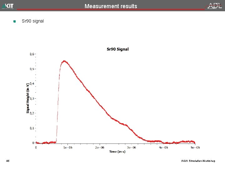
Measurement results Sr 90 signal 45 AIDA Simulation Workshop

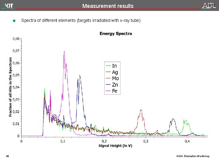
Measurement results Spectra of different elements (targets irradiated with x-ray tube) 46 AIDA Simulation Workshop

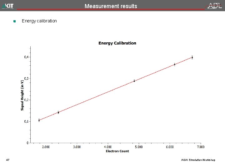
Measurement results Energy calibration 47 AIDA Simulation Workshop

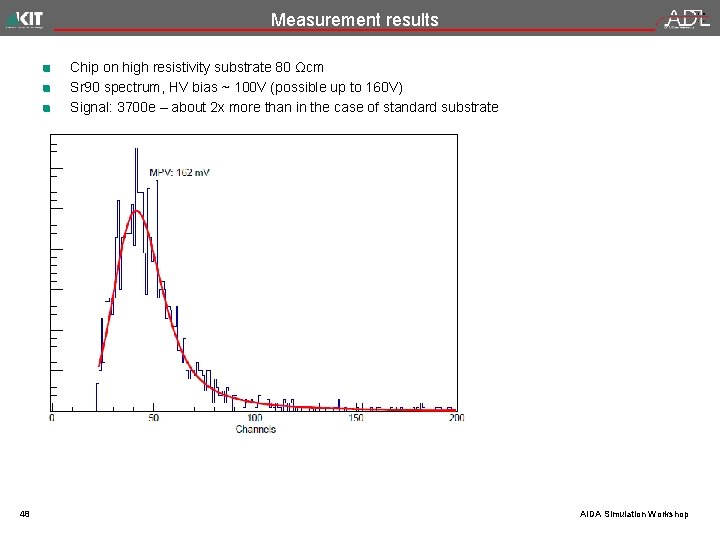
Measurement results Chip on high resistivity substrate 80 Ωcm Sr 90 spectrum, HV bias ~ 100 V (possible up to 160 V) Signal: 3700 e – about 2 x more than in the case of standard substrate 48 AIDA Simulation Workshop

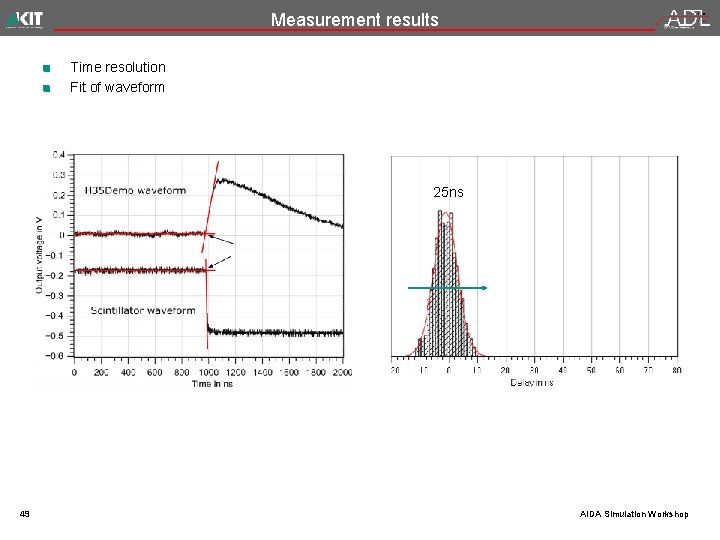
Measurement results Time resolution Fit of waveform 25 ns 49 AIDA Simulation Workshop

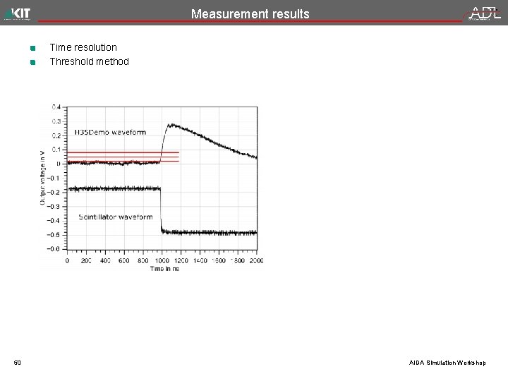
Measurement results Time resolution Threshold method 50 AIDA Simulation Workshop

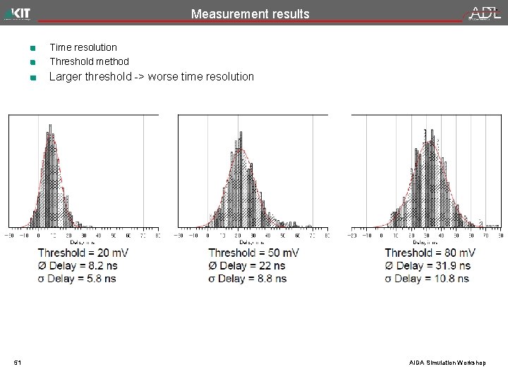
Measurement results Time resolution Threshold method Larger threshold -> worse time resolution 51 AIDA Simulation Workshop

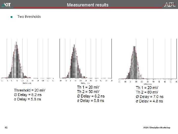
Measurement results Two thresholds 52 AIDA Simulation Workshop

Time Walk Compensating Comparator Ivan Peric KIT – Universität des Landes Baden-Württemberg und nationales Forschungszentrum in der Helmholtz-Gemeinschaft www. kit. edu

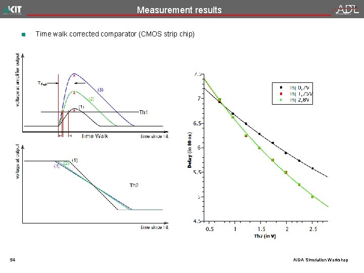
Measurement results Time walk corrected comparator (CMOS strip chip) 54 AIDA Simulation Workshop

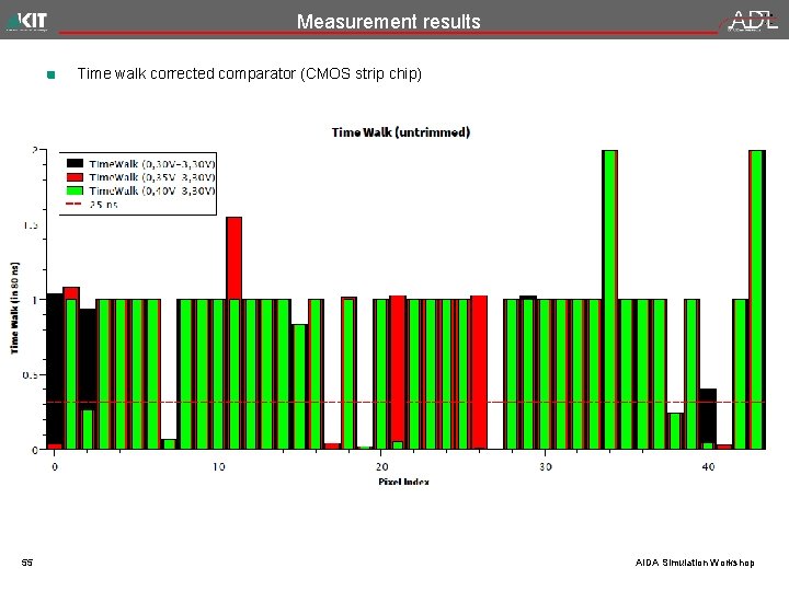
Measurement results Time walk corrected comparator (CMOS strip chip) 55 AIDA Simulation Workshop

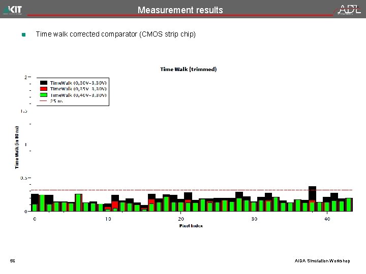
Measurement results Time walk corrected comparator (CMOS strip chip) 56 AIDA Simulation Workshop

HVCMOS – Next Sensors Ivan Peric KIT – Universität des Landes Baden-Württemberg und nationales Forschungszentrum in der Helmholtz-Gemeinschaft www. kit. edu

Monolithic sensor in AMS H 18 technology • • 58 Monolithic sensor in AMS H 18 technology as further development of the Mu 3 e detector Reminder: Mu 3 e monolithic sensor is based on “FEI 3 -architecture” – after hit, a time stamp is stored. All hit data are readout without trigger. The readout of Mu 3 e detector, which includes the 1. 6 Gbit/s links, runs continuously while the sensors are active. Things to improve: 1. Radiation hardness Radiation hardening like in CCPD development: we will use the amplifier of the latest CCPD. 2. Time resolution will be improved by increasing of bias voltage from 60 V to 120 V, by implementing time walk compensation/amplitude measurement and finally by the use of a higher substrate resistivity AIDA Simulation Workshop

Monolithic sensor in AMS H 18 technology • • • • • • 59 AMS: Submission June 2016 Different high resistive substrates Three matrix variants 1. Unbuffered matrix (main option for June) Readout similar like Mu 3 e – four 1. 6 GBit/s links for 4 cm 2. Readout of 4 hits/BC/4 cm 2 possible Time stamp generated in the digital pixel block (hit buffers) -> transfer off chip Hit information x-address, y-address, 10 -bit time stamp, 6 bit amplitude Optional time walk compensation Pixel size around 40 um x 160 um Analog pixels (without comparator), digital periphery -> no crosstalk, low threshold Versatile design, can be used for track trigger or complete by trigger buffer 2. Buffered matrix Readout based on “FEI 4 concept” Group of N pixels (e. g. 8) -> M trigger buffers (e. g. 4) -> readout Pixel size around 40 um x 80 um Digital pixels (with comparator, without clock), buffers on periphery The chip will be able to cope with trigger rate of 5 MHz Trigger buffer is very small in layout (8 um x 80 um) Contains all main features we need for a final design 3. Constant delay multiplexer - like CHESS (small and constant hit-to-output delay - 100 ns) Optimized for easy and fast generartion of track trigger AIDA Simulation Workshop

Monolithic sensor in LFoundry • • 60 LFoundry: Submission July 2016 Goal: Implement the buffered detector version in both technologies AMS and LFoundry for comparison AIDA Simulation Workshop