Status of HVCMOS Developments for ATLAS Ivan Peric



- Slides: 33

Status of HVCMOS Developments for ATLAS Ivan Peric, Roberto Blanco, Felix Ehrler, Christian Krämer, Richard Leys, Rudolf Schimassek, Hui Zhang, … on behalf of University of Bern, Brookhaven National Laboratory, University of Geneva, University of Heidelberg, IFAE, KIT, Lancaster University, University of Liverpool, University of Tsukuba, ANL and UCSC KIT – Universität des Landes Baden-Württemberg und nationales Forschungszentrum in der Helmholtz-Gemeinschaft www. kit. edu

Overview • • 2 CCPD in AMS H 18 HVCMOS technology – test-beam results H 35 DEMO – design and measurement results Monolithic detectors submitted in August 2016 Future plans Pixel 2016

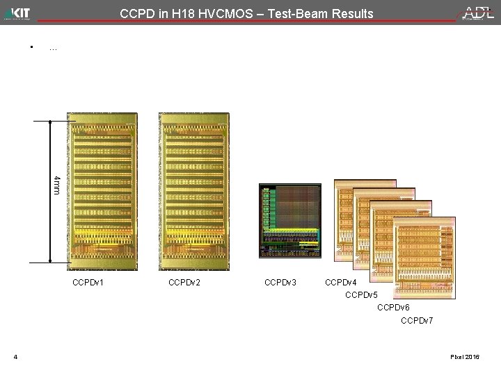
CCPD in H 18 HVCMOS – Test-Beam Results • • • 3 The CCPDv 1 was submitted in November 2011. It is a small HVCMOS test sensor that can be glued to the FEI 4 and readout capacitively. Since then we have had the 7 versions where we improved the circuits The list of improvements is V 1 Basic design V 2 Improved radiation hardness, a few linear transistors replaced with enclosed, better guard rings V 3 CLIC matrix – small pixels V 4 Time encoding pixels V 5 Time walk compensating pixels V 6 Chip version in a. H 18 process based in Austria V 7 Chip version with improved guard ring for higher HV Pixel 2016

CCPD in H 18 HVCMOS – Test-Beam Results • … 4 mm CCPDv 1 CCPDv 2 CCPDv 3 CCPDv 4 CCPDv 5 CCPDv 6 CCPDv 7 4 Pixel 2016

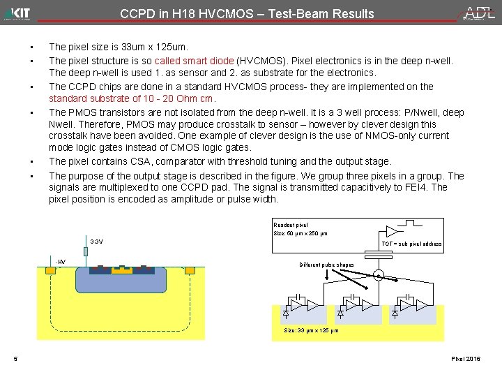
CCPD in H 18 HVCMOS – Test-Beam Results • • • The pixel size is 33 um x 125 um. The pixel structure is so called smart diode (HVCMOS). Pixel electronics is in the deep n-well. The deep n-well is used 1. as sensor and 2. as substrate for the electronics. The CCPD chips are done in a standard HVCMOS process- they are implemented on the standard substrate of 10 - 20 Ohm cm. The PMOS transistors are not isolated from the deep n-well. It is a 3 well process: P/Nwell, deep Nwell. Therefore, PMOS may produce crosstalk to sensor – however by clever design this crosstalk have been avoided. One example of clever design is the use of NMOS-only current mode logic gates instead of CMOS logic gates. The pixel contains CSA, comparator with threshold tuning and the output stage. The purpose of the output stage is described in the figure. We group three pixels in a group. The signals are multiplexed to one CCPD pad. The signal is transmitted capacitively to FEI 4. The pixel position is encoded as amplitude or pulse width. Readout pixel Size: 50 µm x 250 µm 3. 3 V -HV TOT = sub pixel address Different pulse shapes + Size: 33 µm x 125 µm 5 Pixel 2016

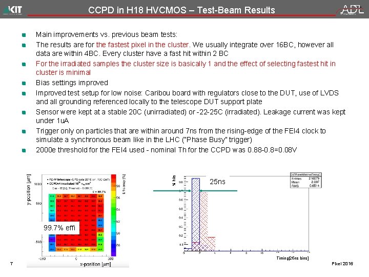
CCPD in H 18 HVCMOS – Test-Beam Results The latest beam result: We measure 99. 7 % efficiency after neutron irradiation to 1015 with the full matrix. The time resolution is excellent. About 84% of the tracks are within 25 ns bin – nearly all within 50 ns. Thresh = 0. 870 V 99. 7% efficiency % hits Bias 25 ns 99. 7% effi Timing[25 ns bins] 6 Pixel 2016

CCPD in H 18 HVCMOS – Test-Beam Results % hits Main improvements vs. previous beam tests: The results are for the fastest pixel in the cluster. We usually integrate over 16 BC, however all data are within 4 BC. Every cluster have a fast hit within 2 BC For the irradiated samples the cluster size is basically 1 and the effect of selecting fastest hit in cluster is minimal Bias settings improved Improved test setup for low noise: Caribou board with regulators close to the DUT, use of LVDS and all grounding referenced locally to the telescope DUT support plate Sensor were kept at a stable 20 C (unirradiated) or -22 -25 C (irradiated). Leakage current was kept under 1 u. A Trigger only on particles that are within around 7 ns from the rising-edge of the FEI 4 clock to simulate a synchronous beam like in the LHC (“Phase Busy” trigger) 2000 e threshold for the FEI 4 used - nominal Th for the CCPD was 0. 88 -0. 8=0. 08 V 25 ns 99. 7% effi Timing[25 ns bins] 7 Pixel 2016

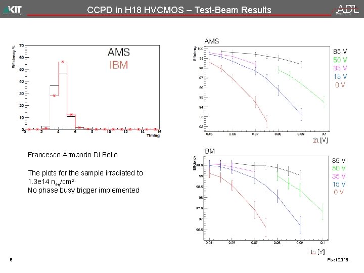
CCPD in H 18 HVCMOS – Test-Beam Results Francesco Armando Di Bello The plots for the sample irradiated to 1. 3 e 14 neq/cm 2. No phase busy trigger implemented 8 Pixel 2016

CCPD - plans • • • 9 We are planning a large version of the CCPD within an AMS H 18 engineering run in November. Rework of the pixel position encoding planned. Pixel size from 25 um x 25 um to 50 um x 250 um Pixel 2016

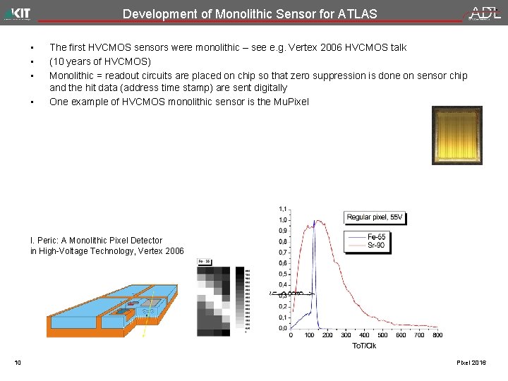
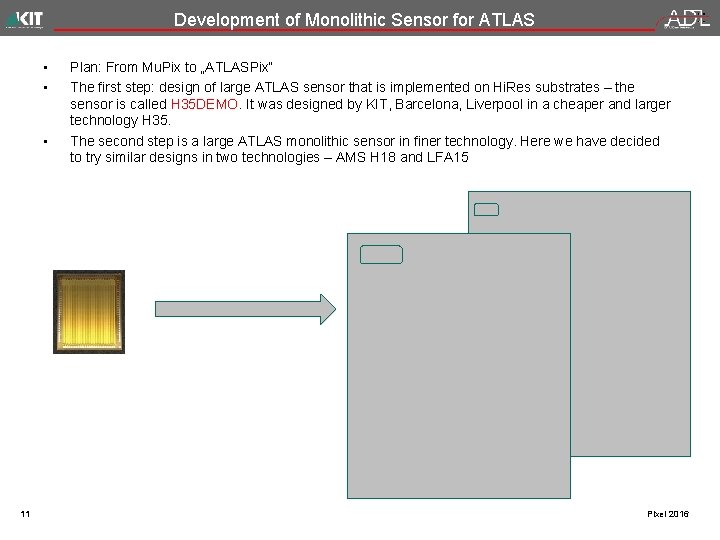
Development of Monolithic Sensor for ATLAS • • The first HVCMOS sensors were monolithic – see e. g. Vertex 2006 HVCMOS talk (10 years of HVCMOS) Monolithic = readout circuits are placed on chip so that zero suppression is done on sensor chip and the hit data (address time stamp) are sent digitally One example of HVCMOS monolithic sensor is the Mu. Pixel I. Peric: A Monolithic Pixel Detector in High-Voltage Technology, Vertex 2006 10 Pixel 2016

Development of Monolithic Sensor for ATLAS • • • 11 Plan: From Mu. Pix to „ATLASPix“ The first step: design of large ATLAS sensor that is implemented on Hi. Res substrates – the sensor is called H 35 DEMO. It was designed by KIT, Barcelona, Liverpool in a cheaper and larger technology H 35. The second step is a large ATLAS monolithic sensor in finer technology. Here we have decided to try similar designs in two technologies – AMS H 18 and LFA 15 Pixel 2016

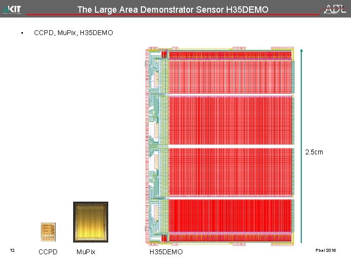
The Large Area Demonstrator Sensor H 35 DEMO • CCPD, Mu. Pix, H 35 DEMO 2. 5 cm 12 CCPD Mu. Pix H 35 DEMO Pixel 2016

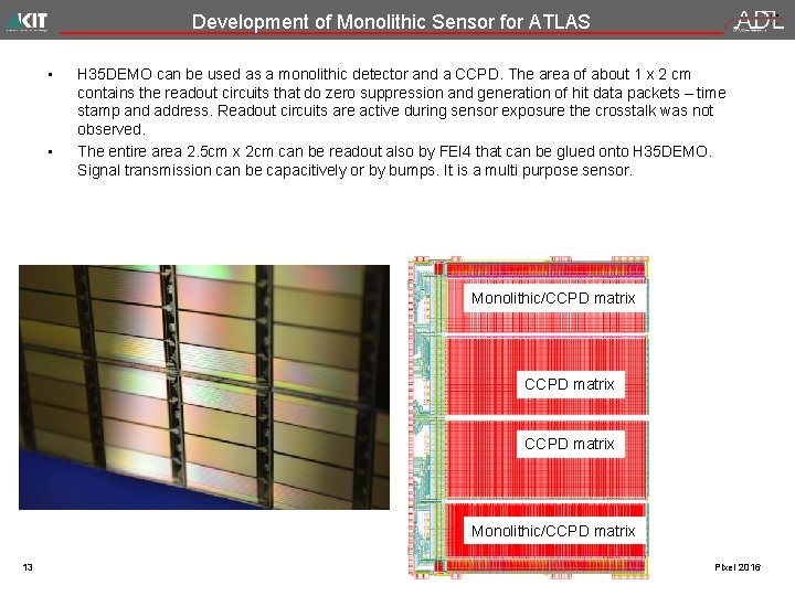
Development of Monolithic Sensor for ATLAS • • H 35 DEMO can be used as a monolithic detector and a CCPD. The area of about 1 x 2 cm contains the readout circuits that do zero suppression and generation of hit data packets – time stamp and address. Readout circuits are active during sensor exposure the crosstalk was not observed. The entire area 2. 5 cm x 2 cm can be readout also by FEI 4 that can be glued onto H 35 DEMO. Signal transmission can be capacitively or by bumps. It is a multi purpose sensor. Monolithic/CCPD matrix Monolithic/CCPD matrix 13 Pixel 2016

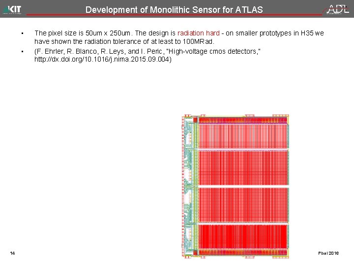
Development of Monolithic Sensor for ATLAS • • 14 The pixel size is 50 um x 250 um. The design is radiation hard - on smaller prototypes in H 35 we have shown the radiation tolerance of at least to 100 MRad. (F. Ehrler, R. Blanco, R. Leys, and I. Peric, “High-voltage cmos detectors, ” http: //dx. doi. org/10. 1016/j. nima. 2015. 09. 004) Pixel 2016

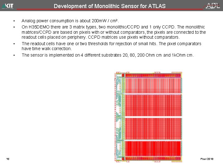
Development of Monolithic Sensor for ATLAS • • 15 Analog power consumption is about 200 m. W / cm 2. On H 35 DEMO there are 3 matrix types, two monolithic/CCPD and 1 only CCPD. The monolithic matrices/CCPD are based on pixels with or without comparators, the pixels are connected to the readout cells placed on periphery. CCPD matrices use pixels without comparators. The readout cells have one or two thresholds for rejection of small hits. The pixel comparators have time walk correction. The sensor is implemented on 4 different substrates 20, 80, 200 Ohm cm and 1 k. Ohm cm. Pixel 2016

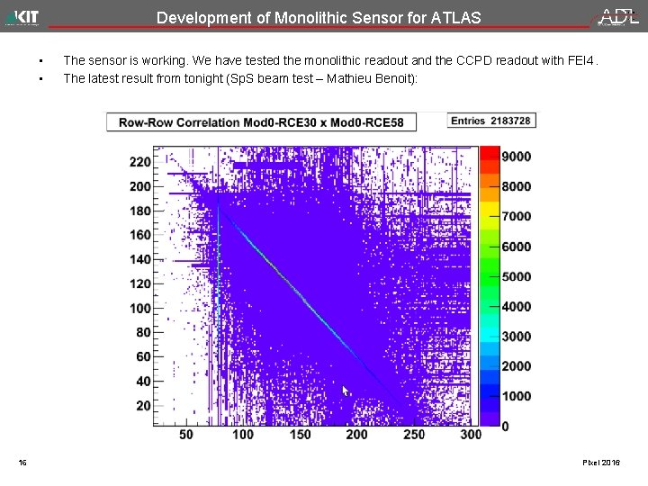
Development of Monolithic Sensor for ATLAS • • 16 The sensor is working. We have tested the monolithic readout and the CCPD readout with FEI 4. The latest result from tonight (Sp. S beam test – Mathieu Benoit): Pixel 2016

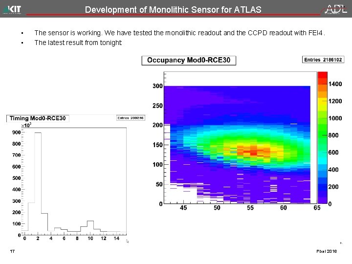
Development of Monolithic Sensor for ATLAS • • 17 The sensor is working. We have tested the monolithic readout and the CCPD readout with FEI 4. The latest result from tonight: Pixel 2016

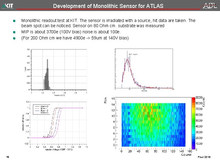
Development of Monolithic Sensor for ATLAS Monolithic readout test at KIT. The sensor is irradiated with a source, hit data are taken. The beam spot can be noticed. Sensor on 80 Ohm cm. substrate was measured MIP is about 3700 e (100 V bias) noise is about 100 e. (For 200 Ohm cm we have 4900 e -> 59 um at 140 V bias) 18 Pixel 2016

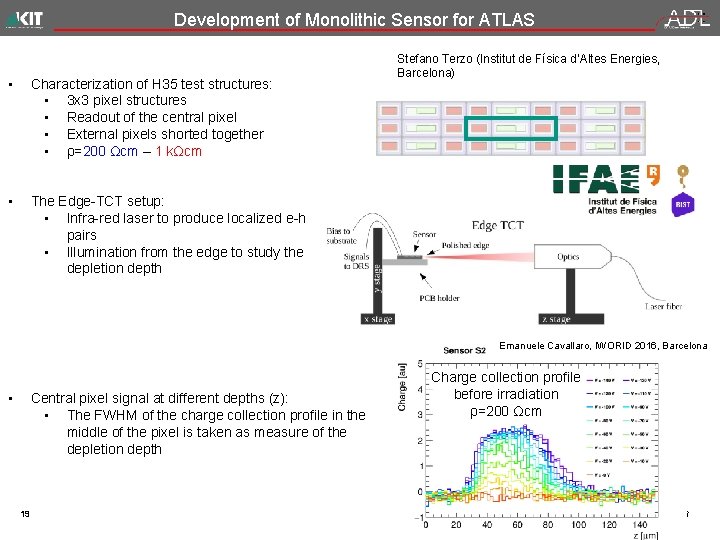
Development of Monolithic Sensor for ATLAS • Characterization of H 35 test structures: • 3 x 3 pixel structures • Readout of the central pixel • External pixels shorted together • ρ=200 Ωcm – 1 kΩcm • The Edge-TCT setup: • Infra-red laser to produce localized e-h pairs • Illumination from the edge to study the depletion depth Stefano Terzo (Institut de Física d’Altes Energies, Barcelona) Emanuele Cavallaro, IWORID 2016, Barcelona • Central pixel signal at different depths (z): • The FWHM of the charge collection profile in the middle of the pixel is taken as measure of the depletion depth 19 Charge collection profile before irradiation ρ=200 Ωcm Pixel 2016

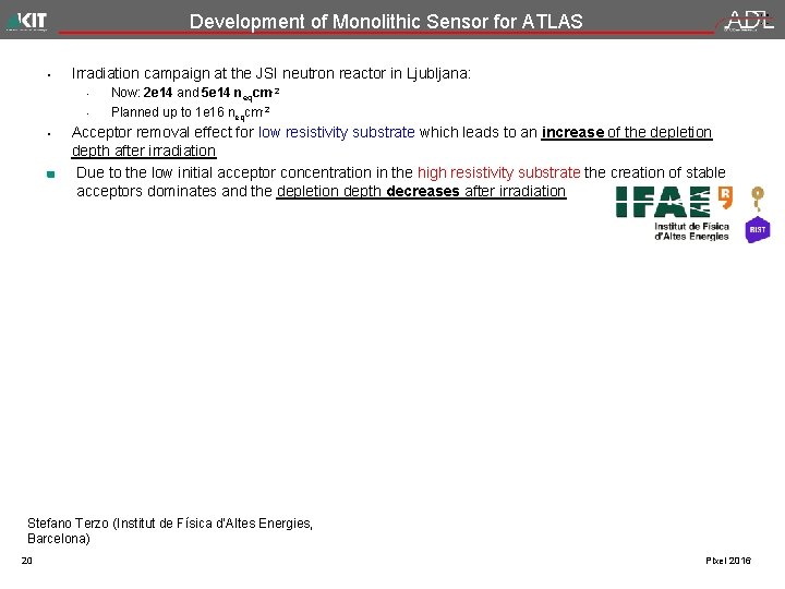
Development of Monolithic Sensor for ATLAS • Irradiation campaign at the JSI neutron reactor in Ljubljana: • • • Now: 2 e 14 and 5 e 14 neqcm-2 Planned up to 1 e 16 neqcm-2 Acceptor removal effect for low resistivity substrate which leads to an increase of the depletion depth after irradiation Due to the low initial acceptor concentration in the high resistivity substrate the creation of stable acceptors dominates and the depletion depth decreases after irradiation Stefano Terzo (Institut de Física d’Altes Energies, Barcelona) 20 Pixel 2016

Development of Monolithic Sensor for ATLAS The sensor works as expected. More results, also on irradiated samples, will be presented In the next stage of our development we are implementing monolithic sensors for ATLAS in finer technologies. We have chosen two technologies AMS H 18 and LFA 15. 21 Pixel 2016

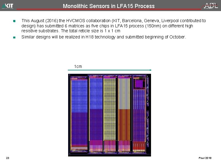
Monolithic Sensors in LFA 15 Process This August (2016) the HVCMOS collaboration (KIT, Barcelona, Geneva, Liverpool contributed to design) has submitted 6 matrices as five chips in LFA 15 process (150 nm) on different high resistive substrates. The total reticle size is 1 x 1 cm Similar designs will be realized in H 18 technology and submitted beginning of October. 22 Pixel 2016

Monolithic Sensors in LFA 15 Process This August (2016) the HVCMOS collaboration (KIT, Barcelona, Geneva, Liverpool contributed to design) has submitted 6 matrices as five chips in LFA 15 process (150 nm) on different high resistive substrates. The total reticle size is 1 x 1 cm Similar designs will be realized in H 18 technology and submitted beginning of October. 1 cm 23 Pixel 2016

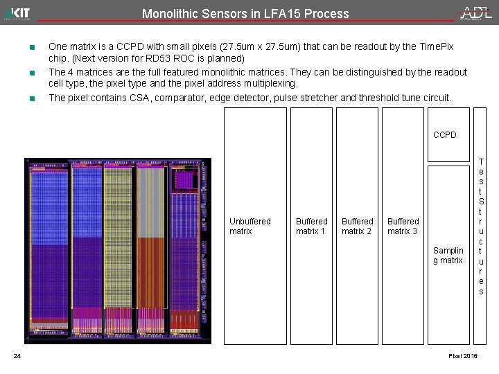
Monolithic Sensors in LFA 15 Process One matrix is a CCPD with small pixels (27. 5 um x 27. 5 um) that can be readout by the Time. Pix chip. (Next version for RD 53 ROC is planned) The 4 matrices are the full featured monolithic matrices. They can be distinguished by the readout cell type, the pixel type and the pixel address multiplexing. The pixel contains CSA, comparator, edge detector, pulse stretcher and threshold tune circuit. CCPD Unbuffered matrix Buffered matrix 1 Buffered matrix 2 Buffered matrix 3 Samplin g matrix 24 Pixel 2016 T e s t S t r u c t u r e s

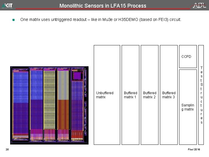
Monolithic Sensors in LFA 15 Process One matrix uses untriggered readout – like in Mu 3 e or H 35 DEMO (based on FEI 3) circuit. CCPD Unbuffered matrix Buffered matrix 1 Buffered matrix 2 Buffered matrix 3 Samplin g matrix 25 Pixel 2016 T e s t S t r u c t u r e s

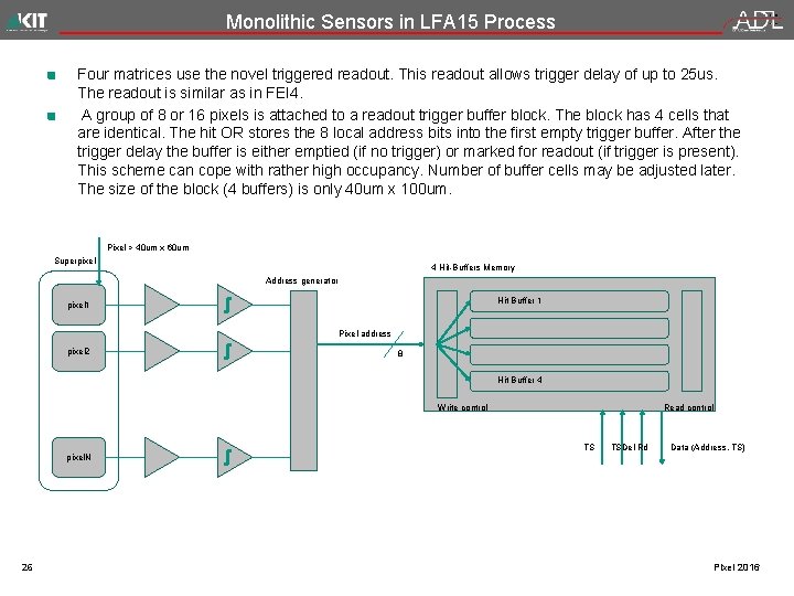
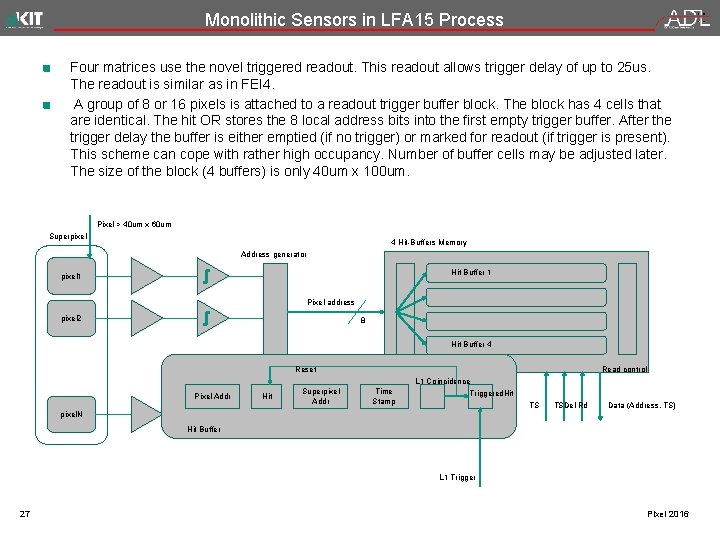
Monolithic Sensors in LFA 15 Process Four matrices use the novel triggered readout. This readout allows trigger delay of up to 25 us. The readout is similar as in FEI 4. A group of 8 or 16 pixels is attached to a readout trigger buffer block. The block has 4 cells that are identical. The hit OR stores the 8 local address bits into the first empty trigger buffer. After the trigger delay the buffer is either emptied (if no trigger) or marked for readout (if trigger is present). This scheme can cope with rather high occupancy. Number of buffer cells may be adjusted later. The size of the block (4 buffers) is only 40 um x 100 um. Pixel > 40 um x 60 um Superpixel 4 Hit-Buffers Memory Address generator Hit Buffer 1 pixel 1 Pixel address pixel 2 8 Hit Buffer 4 Write control Read control TS TSDel Rd Data (Address, TS) pixel. N 26 Pixel 2016

Monolithic Sensors in LFA 15 Process Four matrices use the novel triggered readout. This readout allows trigger delay of up to 25 us. The readout is similar as in FEI 4. A group of 8 or 16 pixels is attached to a readout trigger buffer block. The block has 4 cells that are identical. The hit OR stores the 8 local address bits into the first empty trigger buffer. After the trigger delay the buffer is either emptied (if no trigger) or marked for readout (if trigger is present). This scheme can cope with rather high occupancy. Number of buffer cells may be adjusted later. The size of the block (4 buffers) is only 40 um x 100 um. Pixel > 40 um x 60 um Superpixel 4 Hit-Buffers Memory Address generator Hit Buffer 1 pixel 1 Pixel address pixel 2 8 Hit Buffer 4 Reset Write control Read control L 1 Coincidence Pixel Addr Hit Superpixel Addr Time Stamp Triggered. Hit TS TSDel Rd Data (Address, TS) pixel. N Hit Buffer L 1 Trigger 27 Pixel 2016

Monolithic Sensors in LFA 15 Process As mentioned the number of pixels in the block can be 8 – in this case every pixel has an address bit assigned. The pixel size is 40 x 100 um. In the case of 16 pixels the pixel size is 40 um x 60 um and 16 – 8 address multiplexing is used. The pixel size for untriggered readout is 40 x 100 um. 28 Pixel 2016

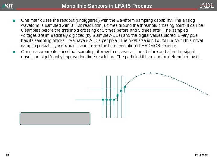
Monolithic Sensors in LFA 15 Process One matrix uses the readout (untriggered) with the waveform sampling capability. The analog waveform is sampled with 8 – bit resolution, 6 times around the threshold crossing point. It can be 6 samples before threshold crossing or 3 times before and 3 times after. The sampled voltages are immediately digitized (by 6 simple ADCs) and the digital values stored. Every pixel has its sampling blocks – we have 6 ADCs per pixel. The pixel size is 40 x 250 um. With this novel sampling capability we would like increase the time resolution of HVCMOS sensors. Our measurements show that sampling of waveform several times before and after the signal onset can significantly improve the time resolution. The particle hit time can be determined by fit. 29 Pixel 2016

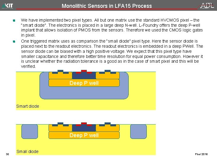
Monolithic Sensors in LFA 15 Process We have implemented two pixel types. All but one matrix use the standard HVCMOS pixel – the “smart diode”. The electronics is placed in a large deep N-well. L-Foundry offers the deep P-well implant that allows isolation of PMOS from the sensors. Therefore we used the CMOS logic gates in pixel. One triggered matrix uses as comparison the “small diode” pixel type. Here the sensor diode is placed next to the readout electronics. The readout electronics is embedded in a deep PWell. The sensor diode can be biased with a high positive voltage. We expect that this pixel type have smaller capacitance and therefore better time resolution for equal power consumption. However it is unclear whether the radiation tolerance is a good as in the case of smart pixel and this will be verified. Deep P well Smart diode Deep P well 30 Small diode Pixel 2016

Monolithic Sensors in LFA 15 Process The chips will be produced in three months As mentioned similar designs will be realized in H 18 technology and submitted beginning of October. The reticle size will be 2 x 2. 5 cm. Half of this run will be covered by the combined Mu 3 e ATLAS sensor. About a half will be the triggered ATLAS designs. One smaller reticle part will be the design that uses the isolated PMOS (fully CMOS) as in the case of LF. 31 Pixel 2016

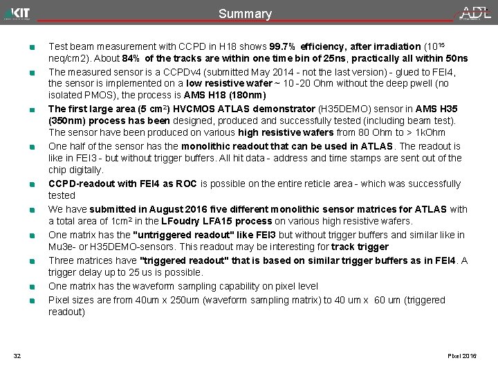
Summary Test beam measurement with CCPD in H 18 shows 99. 7% efficiency, after irradiation (1015 neq/cm 2). About 84% of the tracks are within one time bin of 25 ns, practically all within 50 ns The measured sensor is a CCPDv 4 (submitted May 2014 - not the last version) - glued to FEI 4, the sensor is implemented on a low resistive wafer ~ 10 -20 Ohm without the deep pwell (no isolated PMOS), the process is AMS H 18 (180 nm) The first large area (5 cm 2) HVCMOS ATLAS demonstrator (H 35 DEMO) sensor in AMS H 35 (350 nm) process has been designed, produced and successfully tested (including beam test). The sensor have been produced on various high resistive wafers from 80 Ohm to > 1 k. Ohm One half of the sensor has the monolithic readout that can be used in ATLAS. The readout is like in FEI 3 - but without trigger buffers. All hit data - address and time stamps are sent out of the chip digitally. CCPD-readout with FEI 4 as ROC is possible on the entire reticle area - which was successfully tested We have submitted in August 2016 five different monolithic sensor matrices for ATLAS with a total area of 1 cm 2 in the LFoudry LFA 15 process on various high resistive wafers. One matrix has the "untriggered readout" like FEI 3 but without trigger buffers and similar like in Mu 3 e- or H 35 DEMO-sensors. This readout may be interesting for track trigger Three matrices have "triggered readout" that is based on similar trigger buffers as in FEI 4. A trigger delay up to 25 us is possible. One matrix has the waveform sampling capability on pixel level Pixel sizes are from 40 um x 250 um (waveform sampling matrix) to 40 um x 60 um (triggered readout) 32 Pixel 2016

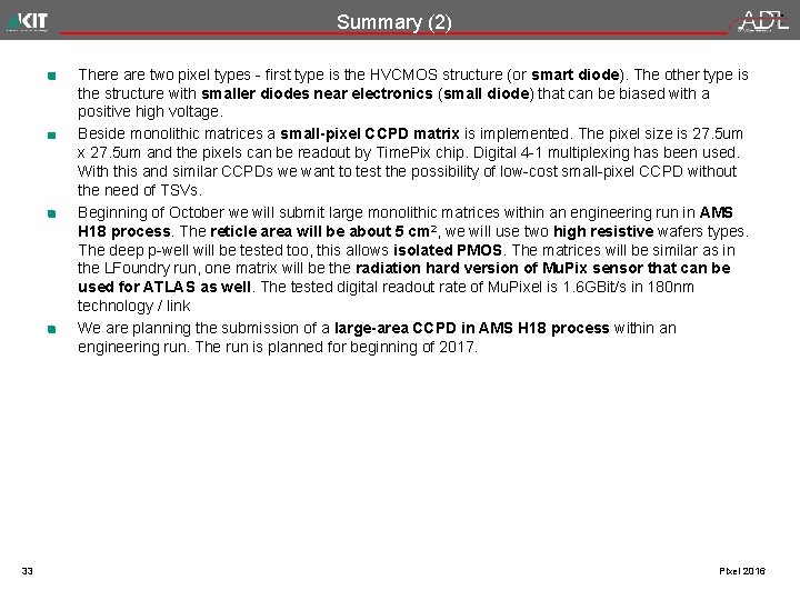
Summary (2) There are two pixel types - first type is the HVCMOS structure (or smart diode). The other type is the structure with smaller diodes near electronics (small diode) that can be biased with a positive high voltage. Beside monolithic matrices a small-pixel CCPD matrix is implemented. The pixel size is 27. 5 um x 27. 5 um and the pixels can be readout by Time. Pix chip. Digital 4 -1 multiplexing has been used. With this and similar CCPDs we want to test the possibility of low-cost small-pixel CCPD without the need of TSVs. Beginning of October we will submit large monolithic matrices within an engineering run in AMS H 18 process. The reticle area will be about 5 cm 2, we will use two high resistive wafers types. The deep p-well will be tested too, this allows isolated PMOS. The matrices will be similar as in the LFoundry run, one matrix will be the radiation hard version of Mu. Pix sensor that can be used for ATLAS as well. The tested digital readout rate of Mu. Pixel is 1. 6 GBit/s in 180 nm technology / link We are planning the submission of a large-area CCPD in AMS H 18 process within an engineering run. The run is planned for beginning of 2017. 33 Pixel 2016