
LHCB Ivan Peric KIT Universitt des Landes BadenWrttemberg
LHCB Ivan Peric KIT – Universität des Landes Baden-Württemberg und nationales Forschungszentrum in der Helmholtz-Gemeinschaft www. kit. edu
t 1 t 2 t 1 t 5 t 5 t 1 t 2 2 t 1 LHCB
t 1 t 1 t 2 t 2 t 1 t 1 t 5 t 5 t 5 t 2 t 1 t 2 t 5 t 5 t 5 3 t 2 t 3 LHCB
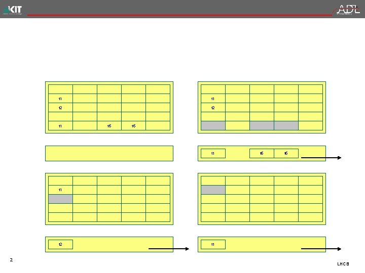
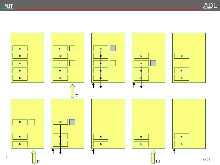
Every pixel has a hit buffer When hit occurs, a time stamp is stored in the hit buffer A priority logic selects the lowest buffer with hit for readout The hit data of the lowest buffers are loaded into end of column cells and transmitted to the digital part. The hit data can belong to different bunch crossings. Only one hit / column is loaded at a time. After transmission of the first group of hits, the remaining hits are copied to eocs. The hits are mixed in time and significant delay happens if there are many hits in a column In the case of large clusters, the readout of all pixels takes time It is difficult to limit the size of the events because the column can contain hits from a large event that we want to discard and hits from a regular event that we don’t want to delete Sorting of hits can be done in the digital part The hits are copied into a content addressable memory. It is important to wait long enough before readout sequence is started in order to assure that all the hits from a particular event passed the end of column logic. Readout sequence All memory entries that have time stamp t 1 are selected (content addressable memory) The selected entries are readout from memory in some order. A token based readout can be used Memory entries with time stamp t 2 are selected and readout Memory entries with time stamp t 3 are “called”. Since there are no corresponding entries, no data will be present at the output bus. Empty event is transmitted 4 LHCB
S 1 S 2 S =1 3 S 4 S =2 5 S 5 t 3 t 2 t 1 5 LHCB
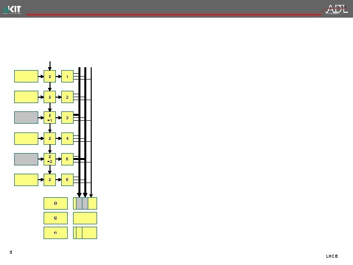
A sort of pipelined data compression logic that generates output synchronous (or with fixed delay) with bunch crossings could be a good choice Example Every pixel can transmit its address via three links Every pixel logic contains an adder that increments the received channel number if there is a hit The channel number is used to select the channel In the figure there are two hits The first hit pixel transmits address (3) via line 1 and the second hit pixel (5) via line 2 In the case of large events (here with more than three hits) overflow flag is generated The pixel addresses and overflow flag, together with bunch crossing ID, are stored for every BX into a FIFO content is transmitted off chip. 6 LHCB
Command receiver and processor Phase det VCO 160 MHz SR sync res 15 Cnt(0 -15) reg 1 clk 40 MHZ BXphas decoder Data, command 7 LHCB
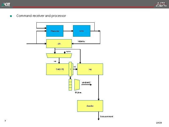
The chip receives commands that are transmitted as bit stream 160 Mbit/2. The commands use special AC balanced encoding, 10 bits are encoded with 16 bits. 160 MHz clock is recovered from the command bit stream. The clock is used for the receiver (A) – the shift register The 160 MHz clock also increments the counter (B) that counts from 0 to 15 From time to time a sync command is sent, when this command is recognized by comparator (C), counter (B) is reset The state 15 of the counter is used to sample the command The second bit of the counter is used to generate 40 MHz BX clock This clock can be delayed in steps of 160 MHz using a shift register 40 MHz clock is used for bunch crossing counter 8 LHCB

Mu. Pix 8 description KIT – Universität des Landes Baden-Württemberg und nationales Forschungszentrum in der Helmholtz-Gemeinschaft www. kit. edu
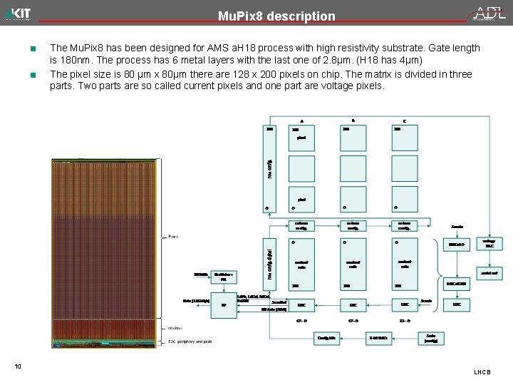
Mu. Pix 8 description The Mu. Pix 8 has been designed for AMS a. H 18 process with high resistivity substrate. Gate length is 180 nm. The process has 6 metal layers with the last one of 2. 8µm. (H 18 has 4µm) The pixel size is 80 µm x 80µm there are 128 x 200 pixels on chip. The matrix is divided in three parts. Two parts are so called current pixels and one part are voltage pixels. 10 LHCB
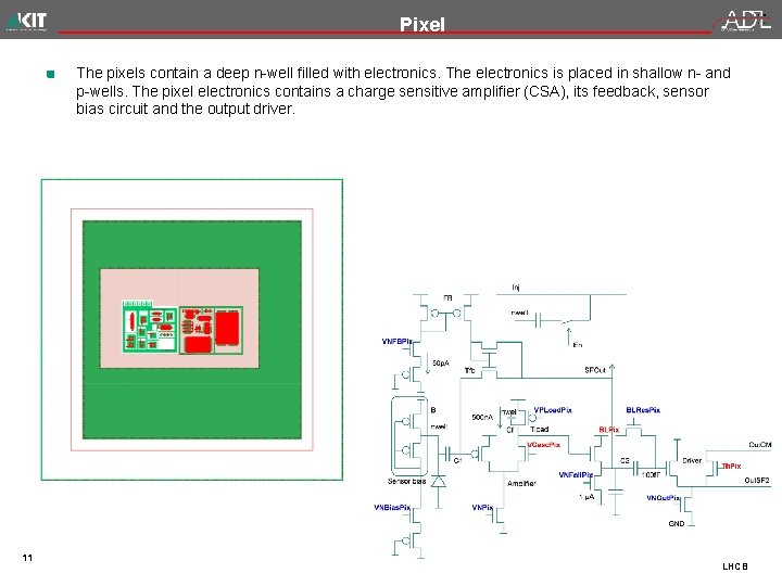
Pixel The pixels contain a deep n-well filled with electronics. The electronics is placed in shallow n- and p-wells. The pixel electronics contains a charge sensitive amplifier (CSA), its feedback, sensor bias circuit and the output driver. 11 LHCB
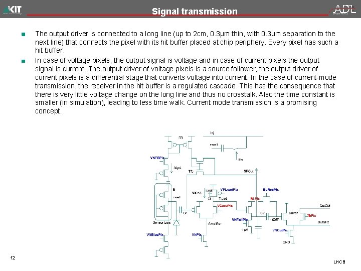
Signal transmission The output driver is connected to a long line (up to 2 cm, 0. 3µm thin, with 0. 3µm separation to the next line) that connects the pixel with its hit buffer placed at chip periphery. Every pixel has such a hit buffer. In case of voltage pixels, the output signal is voltage and in case of current pixels the output signal is current. The output driver of voltage pixels is a source follower, the output driver of current pixels is a differential stage that converts voltage into current. In the case of current-mode transmission, the receiver in the hit buffer is a regulated cascade. This has the consequence that there is very little voltage change on the long line and thus no crosstalk. Also the time constant is smaller (in simulation), leading to less time walk. Current mode transmission is a promising concept. 12 LHCB
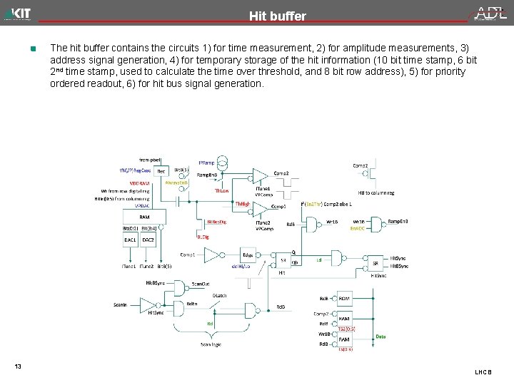
Hit buffer The hit buffer contains the circuits 1) for time measurement, 2) for amplitude measurements, 3) address signal generation, 4) for temporary storage of the hit information (10 bit time stamp, 6 bit 2 nd time stamp, used to calculate the time over threshold, and 8 bit row address), 5) for priority ordered readout, 6) for hit bus signal generation. 13 LHCB
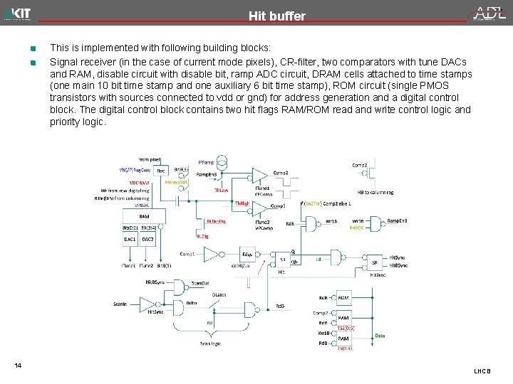
Hit buffer This is implemented with following building blocks: Signal receiver (in the case of current mode pixels), CR-filter, two comparators with tune DACs and RAM, disable circuit with disable bit, ramp ADC circuit, DRAM cells attached to time stamps (one main 10 bit time stamp and one auxiliary 6 bit time stamp), ROM circuit (single PMOS transistors with sources connected to vdd or gnd) for address generation and a digital control block. The digital control block contains two hit flags RAM/ROM read and write control logic and priority logic. 14 LHCB
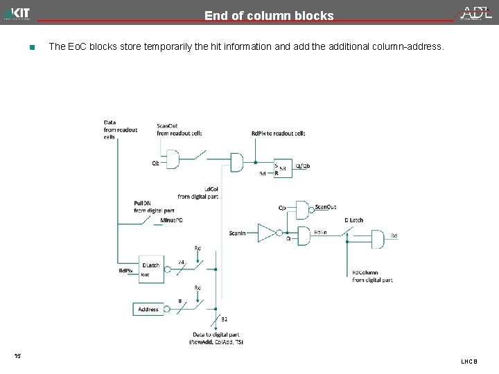
End of column blocks The Eo. C blocks store temporarily the hit information and add the additional column-address. 15 LHCB
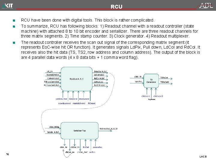
RCU have been done with digital tools. This block is rather complicated. To summarize, RCU has following blocks: 1) Readout channel with a readout controller (state machine) with attached 8 to 10 bit encoder and seriallizer. There are three readout channels for three matrix segments. 2) Time stamp counter. 3) Clock generator. 4) Readout multiplexer. The readout controller receives the scan out signal of the corresponding matrix segment (it represents Eo. C-wise hit OR function). It generates signals Ld. Pix, Pull down, Ld. Col and Rd. Col. It receives also the hit data (TS, TS 2, row address and column address). The output of the block is are 4 parallel data words (4 x 8 data bits + 1 comma word flag). 16 LHCB
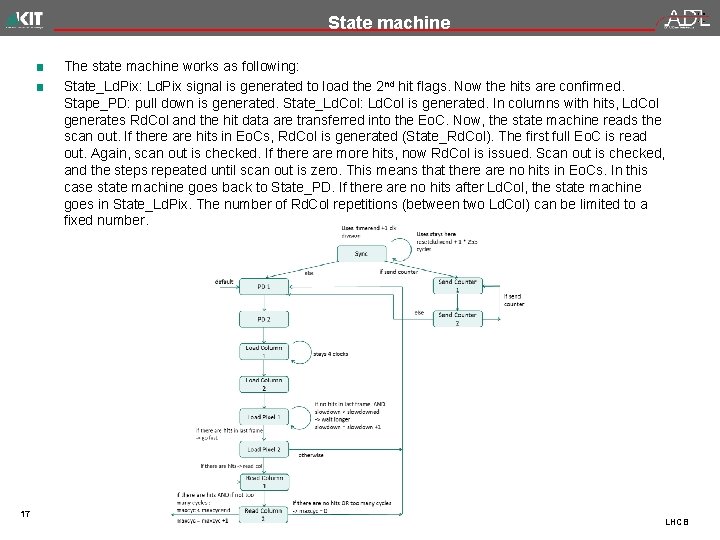
State machine The state machine works as following: State_Ld. Pix: Ld. Pix signal is generated to load the 2 nd hit flags. Now the hits are confirmed. Stape_PD: pull down is generated. State_Ld. Col: Ld. Col is generated. In columns with hits, Ld. Col generates Rd. Col and the hit data are transferred into the Eo. C. Now, the state machine reads the scan out. If there are hits in Eo. Cs, Rd. Col is generated (State_Rd. Col). The first full Eo. C is read out. Again, scan out is checked. If there are more hits, now Rd. Col is issued. Scan out is checked, and the steps repeated until scan out is zero. This means that there are no hits in Eo. Cs. In this case state machine goes back to State_PD. If there are no hits after Ld. Col, the state machine goes in State_Ld. Pix. The number of Rd. Col repetitions (between two Ld. Col) can be limited to a fixed number. 17 LHCB
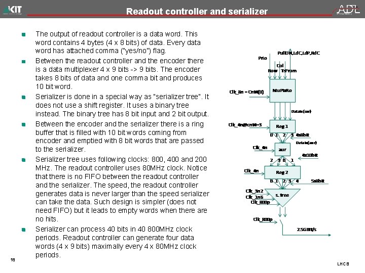
Readout controller and serializer 18 The output of readout controller is a data word. This word contains 4 bytes (4 x 8 bits) of data. Every data word has attached comma (“yes/no”) flag. Between the readout controller and the encoder there is a data multiplexer 4 x 9 bits -> 9 bits. The encoder takes 8 bits of data and one comma bit and produces 10 bit word. Serializer is done in a special way as “serializer tree”. It does not use a shift register. It uses a binary tree instead. The binary tree has 8 bit input and 2 bit output. Between the encoder and the serializer there is a ring buffer that is filled with 10 bit words coming from encoder and emptied with 8 bit words that are passed to the serializer. Serializer tree uses following clocks: 800, 400 and 200 MHz. The readout controller uses 80 MHz clock. Notice that there is no FIFO between the readout controller and the serializer. The speed, the readout controller generates data is never larger than the speed serializer can take the data. Such design is simpler (does not need FIFO) but it leads to empty words when there are no hits. Serializer can process 40 bits in 40 800 MHz clock periods. Readout controller can generate four data words (4 x 9 bits) maximally every 4 x 80 MHz clock periods. LHCB
Time stamp frequency The time stamp generator runs with 160 MHz clock. (Notice that the system does not have a 250 MHz clock, it has only 200 MHz and 160 MHz clocks. ) 19 LHCB
Small blocks Registers There are several configuration registers on chip: row configuration register, column configuration register, hit buffer configuration register, bias block configuration register 2 x. All these registers use full custom made cells The register interface has following signals: Ck 1, Sin, Sout, Rb and Load. These signals are connected to analogue pads. Current mode DACs with bias “diodes” Current mode DACs are 6 -bit DACs made with current sources. These DACs produce currents. To bias a current source in a pixel, there is a diode connected transistor near the DAC. The DAC current makes voltage when it flows through the diode-connected device. The voltage is distributed in pixels and connected to the gates of the current sources. Reference current generator The bias voltage for the current sources in the current mode DACs can be generated by a bandgap reference circuit or by a resistor. Reference circuit generates as first a voltage. This voltage is converted to current and the current is flowing through a diode connected MOSFET. Voltage mode DAC Digital drivers LVDS in and out cells Analog and hit bus buffer Temperature measurement circuit Pads Following pads are used: analogue pad, no protection pad. The pads are grouped into analogue and digital domain. 20 LHCB
- Slides: 20