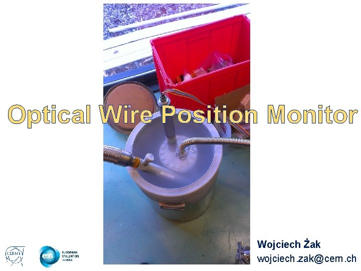
Optical Wire Position Monitor Wojciech ak wojciech zakcern
![First test at cold with movable wire 6. 000 5. 000 Voltage [V] 4. First test at cold with movable wire 6. 000 5. 000 Voltage [V] 4.](https://slidetodoc.com/presentation_image_h/d0daae73b380e5ae172c59ce9accc0cb/image-21.jpg)
![Voltage [V] 0 -5 E-05 -0. 0001 -0. 00025 06/08/2014 13: 43: 11: 552 Voltage [V] 0 -5 E-05 -0. 0001 -0. 00025 06/08/2014 13: 43: 11: 552](https://slidetodoc.com/presentation_image_h/d0daae73b380e5ae172c59ce9accc0cb/image-30.jpg)

- Slides: 34

Optical Wire Position Monitor Wojciech Żak wojciech. zak@cern. ch

Outline • • • Application of the OPWM in the SPL Mock-up Idea of the Optical Wire Position Monitor Conception tests and calibration at warm Tests at liquid nitrogen Behavior of components with temperature Conclusions

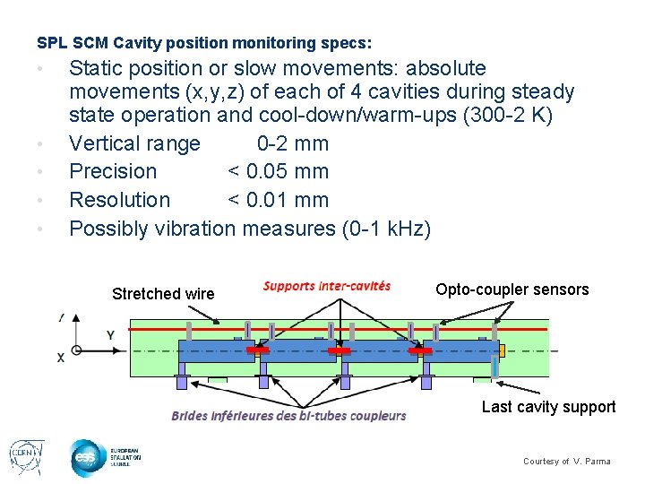
SPL SCM Cavity position monitoring specs: • • • Static position or slow movements: absolute movements (x, y, z) of each of 4 cavities during steady state operation and cool-down/warm-ups (300 -2 K) Vertical range 0 -2 mm Precision < 0. 05 mm Resolution < 0. 01 mm Possibly vibration measures (0 -1 k. Hz) Stretched wire Opto-coupler sensors Last cavity support Courtesy of V. Parma

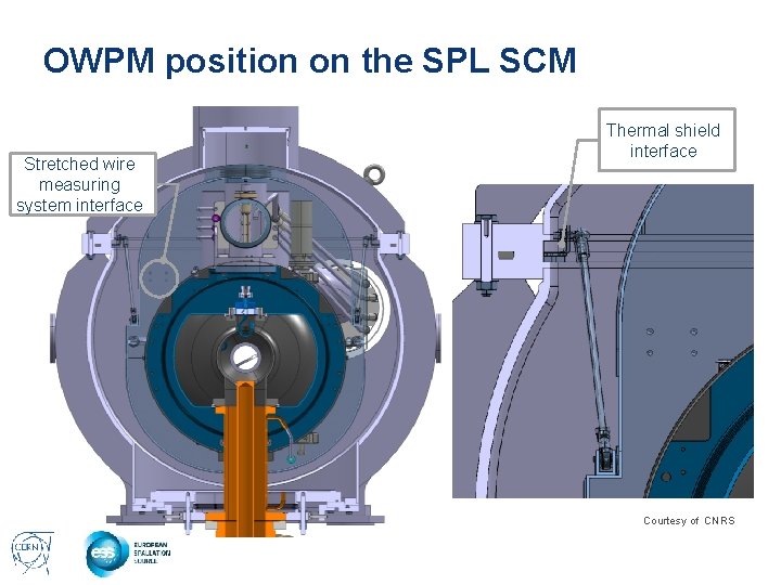
OWPM position on the SPL SCM Stretched wire measuring system interface Thermal shield interface Courtesy of CNRS

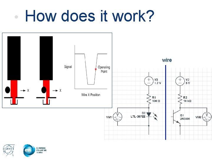
• How does it work? wire

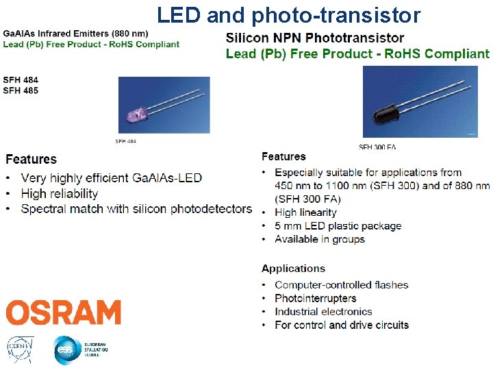
LED and photo-transistor

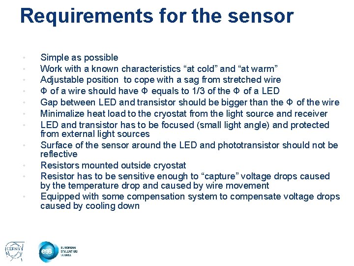
Requirements for the sensor • • • Simple as possible Work with a known characteristics “at cold” and “at warm” Adjustable position to cope with a sag from stretched wire Φ of a wire should have Φ equals to 1/3 of the Φ of a LED Gap between LED and transistor should be bigger than the Φ of the wire Minimalize heat load to the cryostat from the light source and receiver LED and transistor has to be focused (small light angle) and protected from external light sources Surface of the sensor around the LED and phototransistor should not be reflective Resistors mounted outside cryostat Resistor has to be sensitive enough to “capture” voltage drops caused by the temperature drop and caused by wire movement Equipped with some compensation system to compensate voltage drops caused by cooling down

Expectations about the first tests Prove the concept • Characterize LEDs and phototransistors at room temperature •

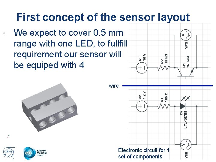
First concept of the sensor layout • We expect to cover 0. 5 mm range with one LED, to fullfill requirement our sensor will be equiped with 4 wire Electronic circuit for 1 set of components

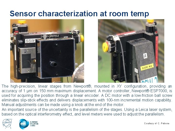
Sensor characterization at room temp The high-precision, linear stages from Newport®, mounted in XY configuration, providing an accuracy of 1 µm on 150 mm maximum displacement. A motor controller, Newport® ESP 7000, is used for acquiring the position through a linear encoder. A DC motor with a low-friction ball screw eliminates slip-stick effects and delivers displacements with 100 -nm incremental motion capability. Manual adjustments can be made using a knob at the end of the motor. An important source of the uncertainty is the parallelism of the stages. Using a Leica laser system, based on the optical interferometry effect, and level meters were used to adjust the parallelism. Courtesy of C. Petrone

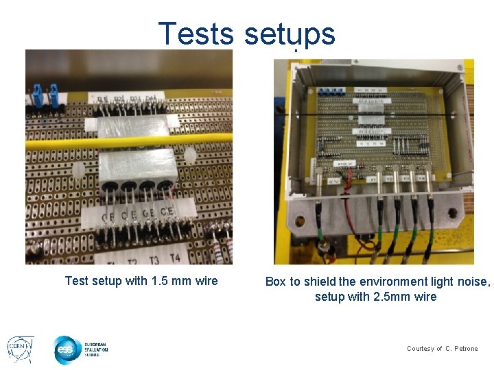
Tests setups Test setup with 1. 5 mm wire Box to shield the environment light noise, setup with 2. 5 mm wire Courtesy of C. Petrone

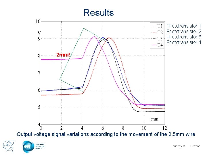
Results Phototransistor 1 Phototransistor 2 Phototransistor 3 Phototransistor 4 2 mm! Output voltage signal variations according to the movement of the 2. 5 mm wire Courtesy of C. Petrone

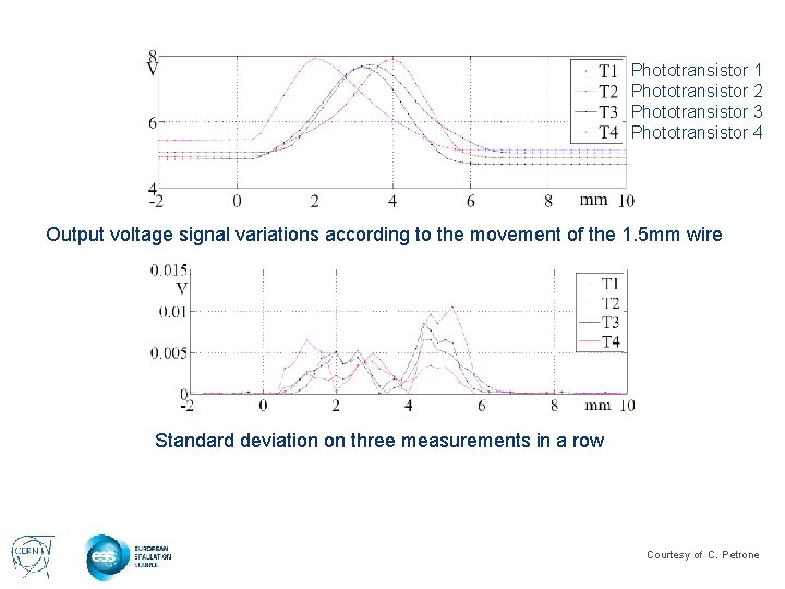
Phototransistor 1 Phototransistor 2 Phototransistor 3 Phototransistor 4 Output voltage signal variations according to the movement of the 1. 5 mm wire Standard deviation on three measurements in a row Courtesy of C. Petrone

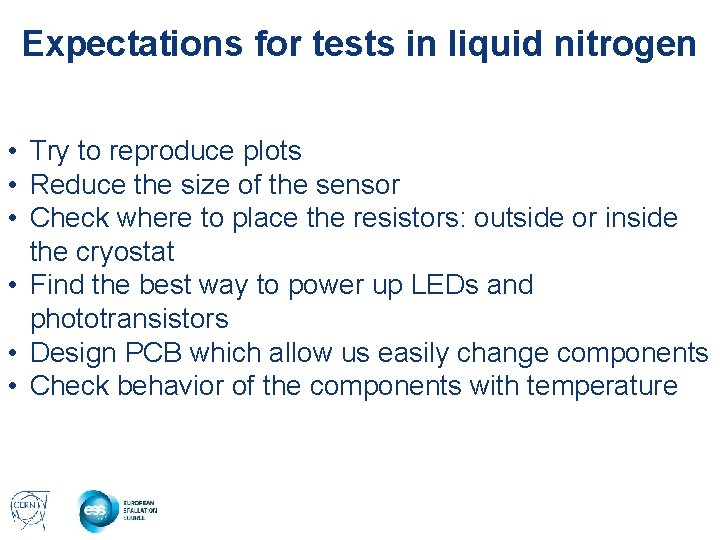
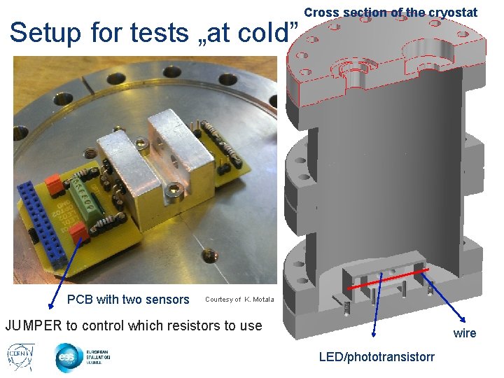
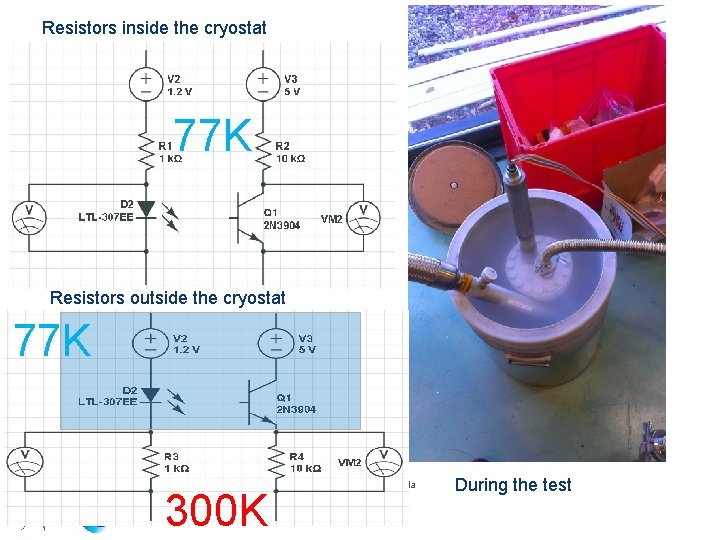
Expectations for tests in liquid nitrogen • Try to reproduce plots • Reduce the size of the sensor • Check where to place the resistors: outside or inside the cryostat • Find the best way to power up LEDs and phototransistors • Design PCB which allow us easily change components • Check behavior of the components with temperature

Setup for tests „at cold” PCB with two sensors Cross section of the cryostat Courtesy of K. Motala JUMPER to control which resistors to use wire LED/phototransistorr

Resistors inside the cryostat 77 K Resistors outside the cryostat 77 K 300 K Courtesy of K. Motala During the test

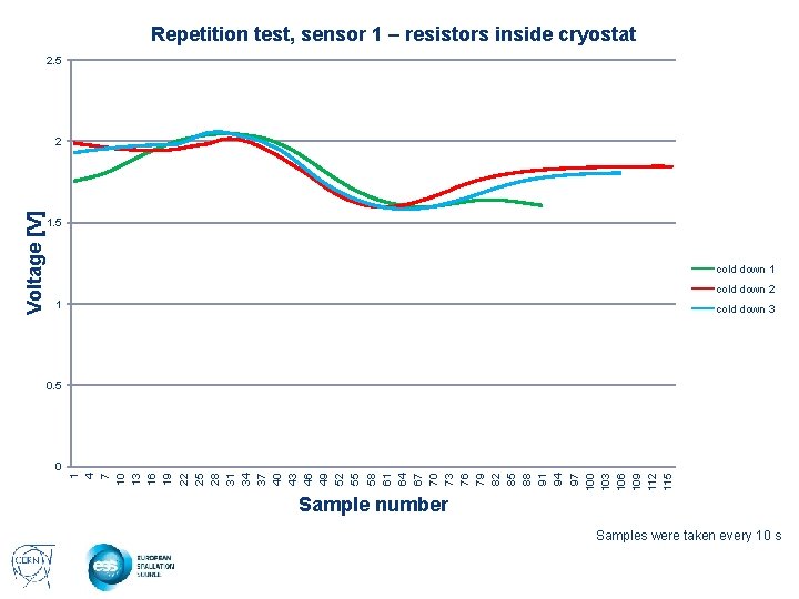
Repetition test, sensor 1 – resistors inside cryostat 2. 5 1. 5 cold down 1 cold down 2 1 cold down 3 0. 5 0 1 4 7 10 13 16 19 22 25 28 31 34 37 40 43 46 49 52 55 58 61 64 67 70 73 76 79 82 85 88 91 94 97 100 103 106 109 112 115 Voltage [V] 2 Sample number Samples were taken every 10 s

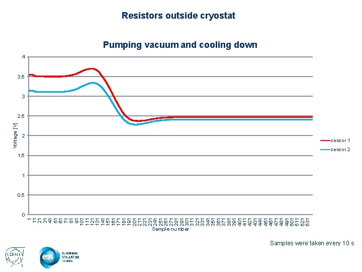
0 1 11 21 31 41 51 61 71 81 91 101 111 121 131 141 151 161 171 181 191 201 211 221 231 241 251 261 271 281 291 301 311 321 331 341 351 361 371 381 391 401 411 421 431 441 451 461 471 481 491 501 511 521 531 Voltage [V] Resistors outside cryostat Pumping vacuum and cooling down 4 3. 5 3 2. 5 2 sensor 1 1. 5 sensor 2 1 0. 5 Sample number Samples were taken every 10 s

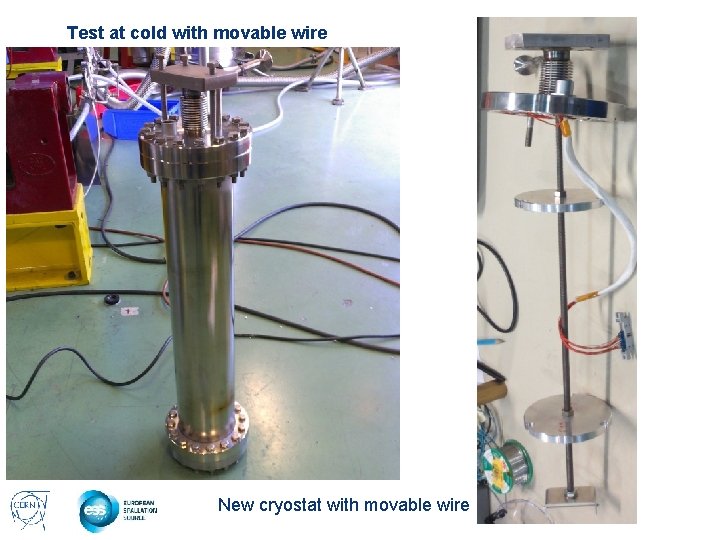
Test at cold with movable wire New cryostat with movable wire

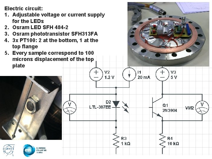
Electric circuit: 1. Adjustable voltage or current supply for the LEDs 2. Osram LED SFH 484 -2 3. Osram phototransistor SFH 313 FA 4. 3 x PT 100: 2 at the bottom, 1 at the top flange 5. Every sample correspond to 100 microns displacement of the top plate
![First test at cold with movable wire 6 000 5 000 Voltage V 4 First test at cold with movable wire 6. 000 5. 000 Voltage [V] 4.](https://slidetodoc.com/presentation_image_h/d0daae73b380e5ae172c59ce9accc0cb/image-21.jpg)
First test at cold with movable wire 6. 000 5. 000 Voltage [V] 4. 000 1 2 3. 000 3 c 1 c 2 2. 000 1. 000 0. 000 1 2 3 4 5 6 7 8 9 101112131415161718192021222324252627282930313233343536373839404142434445 Sample number

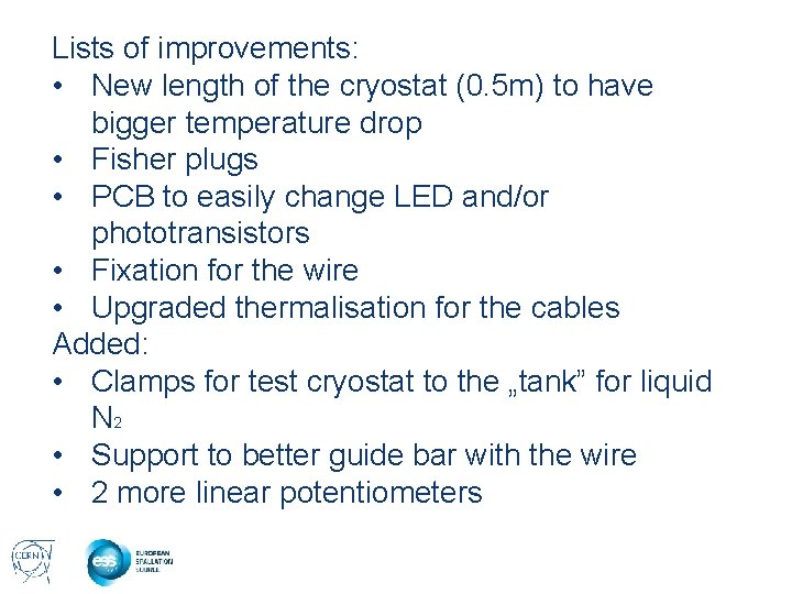
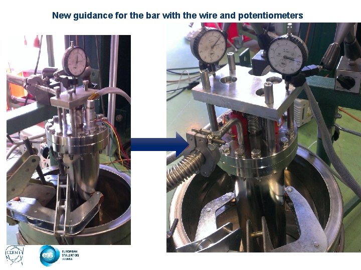
Lists of improvements: • New length of the cryostat (0. 5 m) to have bigger temperature drop • Fisher plugs • PCB to easily change LED and/or phototransistors • Fixation for the wire • Upgraded thermalisation for the cables Added: • Clamps for test cryostat to the „tank” for liquid N 2 • Support to better guide bar with the wire • 2 more linear potentiometers

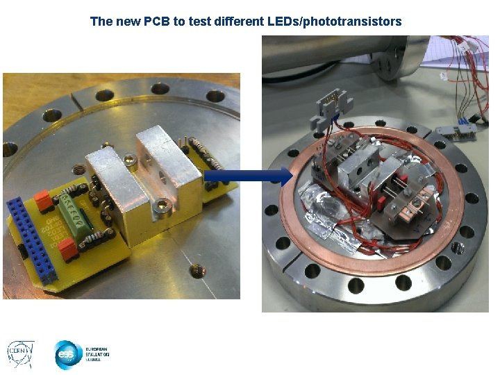
The new PCB to test different LEDs/phototransistors

New guidance for the bar with the wire and potentiometers

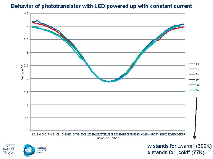
Behavior of phototransistor with LED powered up with constant current 4. 5 4 3. 5 Voltage [V] 3 1 c 2. 5 2 c 3 c 2 1 w 2 w 3 w 1. 5 1 0. 5 0 1 2 3 4 5 6 7 8 9101112131415161718192021222324252627282930313233343536373839404142434445464748495051525354555657 sample number w stands for „warm” (300 K) c stands for „cold” (77 K)

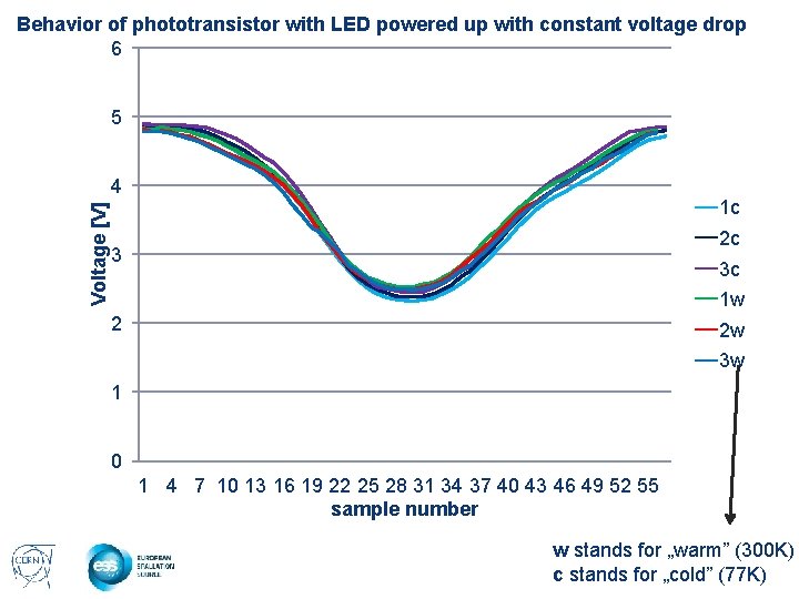
Behavior of phototransistor with LED powered up with constant voltage drop 6 5 Voltage [V] 4 1 c 2 c 3 3 c 1 w 2 2 w 3 w 1 0 1 4 7 10 13 16 19 22 25 28 31 34 37 40 43 46 49 52 55 sample number w stands for „warm” (300 K) c stands for „cold” (77 K)

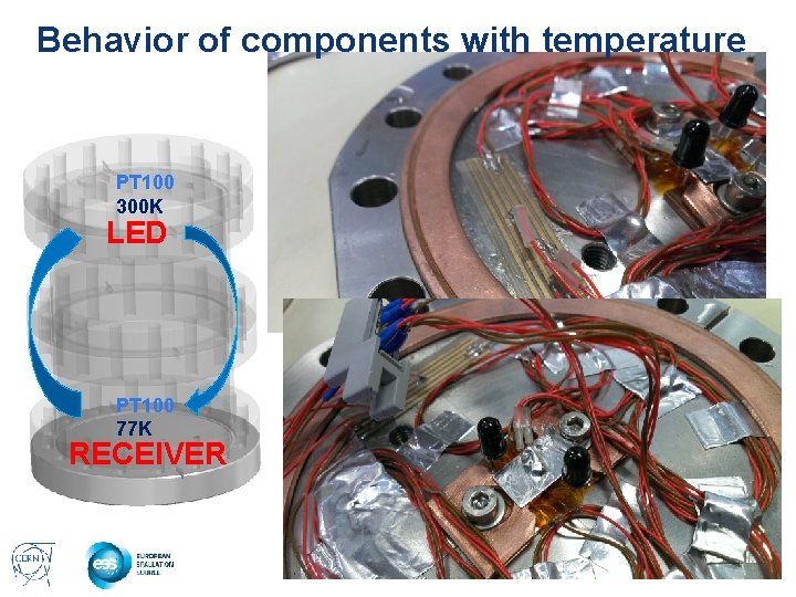
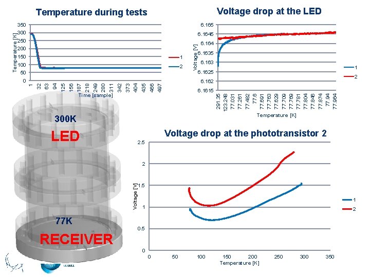
Behavior of components with temperature PT 100 300 K LED PT 100 77 K RECEIVER

Voltage drop at the LED 350 6. 165 300 6. 1645 200 150 1 100 2 6. 164 6. 1635 6. 163 1 6. 1625 2 6. 1615 Time [sample] 291. 35 123. 248 77. 031 77. 261 77. 482 77. 691 77. 763 77. 629 77. 709 77. 769 77. 781 77. 804 77. 846 77. 874 77. 964 6. 162 497 466 435 404 373 342 311 280 249 218 187 156 94 63 32 0 125 50 Voltage [V] 250 Temperature [K] 300 K Voltage drop at the phototransistor 2 LED 2. 5 2 Voltage [V] 1 Temperature [K] Temperature during tests 77 K RECEIVER 1. 5 1 1 2 0. 5 0 0 50 100 150 200 Temperature [K] 250 300 350

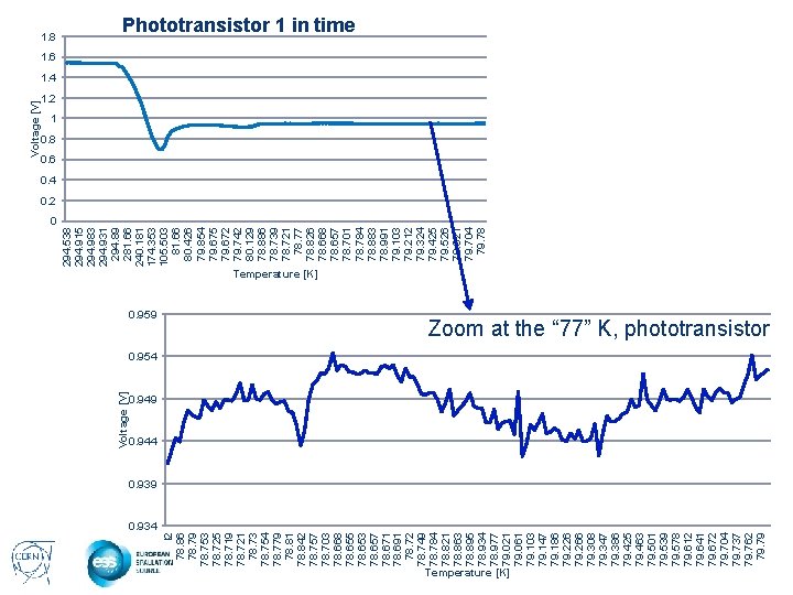
0. 959 0. 934 78. 942 78. 86 78. 79 78. 753 78. 725 78. 719 78. 721 78. 73 78. 754 78. 779 78. 81 78. 842 78. 757 78. 703 78. 668 78. 655 78. 653 78. 657 78. 671 78. 691 78. 72 78. 749 78. 784 78. 821 78. 863 78. 895 78. 934 78. 977 79. 021 79. 061 79. 103 79. 147 79. 186 79. 226 79. 266 79. 308 79. 347 79. 386 79. 425 79. 463 79. 501 79. 539 79. 578 79. 612 79. 641 79. 672 79. 704 79. 737 79. 762 79. 79 Voltage [V] 0 294. 538 294. 915 294. 983 294. 931 294. 89 281. 66 240. 181 174. 353 105. 503 81. 66 80. 426 79. 854 79. 675 79. 672 79. 742 80. 129 78. 886 78. 739 78. 721 78. 77 78. 826 78. 668 78. 657 78. 701 78. 784 78. 883 78. 991 79. 103 79. 212 79. 324 79. 425 79. 526 79. 621 79. 704 79. 78 Voltage [V] 1. 8 Phototransistor 1 in time 1. 6 1. 4 1. 2 1 0. 8 0. 6 0. 4 0. 2 Temperature [K] Zoom at the “ 77” K, phototransistor 0. 954 0. 949 0. 944 0. 939 Temperature [K]
![Voltage V 0 5 E05 0 0001 0 00025 06082014 13 43 11 552 Voltage [V] 0 -5 E-05 -0. 0001 -0. 00025 06/08/2014 13: 43: 11: 552](https://slidetodoc.com/presentation_image_h/d0daae73b380e5ae172c59ce9accc0cb/image-30.jpg)
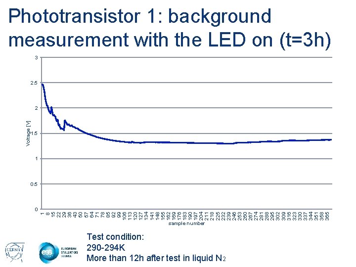
Voltage [V] 0 -5 E-05 -0. 0001 -0. 00025 06/08/2014 13: 43: 11: 552 06/08/2014 14: 08: 11: 276 06/08/2014 14: 33: 11: 276 06/08/2014 14: 58: 11: 276 06/08/2014 15: 23: 11: 276 06/08/2014 15: 48: 17: 676 06/08/2014 16: 13: 17: 676 06/08/2014 16: 38: 17: 676 06/08/2014 17: 03: 17: 676 06/08/2014 17: 28: 14: 076 06/08/2014 17: 53: 14: 076 06/08/2014 18: 43: 14: 076 06/08/2014 19: 08: 14: 076 06/08/2014 19: 33: 20: 476 06/08/2014 19: 58: 20: 476 06/08/2014 20: 23: 20: 476 06/08/2014 20: 48: 20: 476 06/08/2014 21: 13: 16: 876 06/08/2014 21: 38: 16: 876 06/08/2014 22: 03: 16: 876 06/08/2014 22: 28: 16: 876 06/08/2014 22: 53: 13: 276 06/08/2014 23: 18: 13: 276 06/08/2014 23: 43: 13: 276 07/08/2014 00: 08: 13: 276 07/08/2014 00: 33: 13: 276 07/08/2014 00: 58: 19: 676 07/08/2014 01: 23: 19: 676 07/08/2014 01: 48: 19: 676 07/08/2014 02: 13: 19: 676 07/08/2014 02: 38: 16: 076 07/08/2014 03: 28: 16: 076 07/08/2014 03: 53: 16: 076 07/08/2014 04: 18: 12: 476 07/08/2014 04: 43: 12: 476 07/08/2014 05: 08: 12: 476 07/08/2014 05: 33: 12: 476 07/08/2014 05: 58: 12: 476 07/08/2014 06: 23: 18: 876 07/08/2014 06: 48: 18: 876 07/08/2014 07: 13: 18: 876 07/08/2014 07: 38: 18: 876 07/08/2014 08: 03: 15: 276 07/08/2014 08: 28: 15: 276 07/08/2014 08: 53: 15: 276 07/08/2014 09: 18: 15: 276 07/08/2014 09: 43: 15: 276 07/08/2014 10: 08: 11: 676 07/08/2014 10: 33: 11: 677 07/08/2014 10: 58: 11: 676 07/08/2014 11: 23: 11: 676 07/08/2014 11: 48: 18: 076 07/08/2014 12: 13: 18: 076 07/08/2014 12: 38: 18: 076 07/08/2014 13: 03: 18: 076 07/08/2014 13: 28: 14: 476 Background measurements 0. 0002 0. 00015 0. 0001 5 E-05 -0. 00015 -0. 0002 Time

0 1 8 15 22 29 36 43 50 57 64 71 78 85 92 99 106 113 120 127 134 141 148 155 162 169 176 183 190 197 204 211 218 225 232 239 246 253 260 267 274 281 288 295 302 309 316 323 330 337 344 351 358 365 Voltage [V] Phototransistor 1: background measurement with the LED on (t=3 h) 3 2. 5 2 1. 5 1 0. 5 sample number Test condition: 290 -294 K More than 12 h after test in liquid N 2

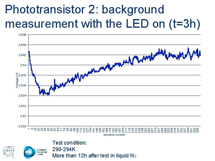
Phototransistor 2: background measurement with the LED on (t=3 h) 2. 546 2. 544 2. 542 2. 538 2. 536 2. 534 2. 532 2. 53 2. 528 1 8 15 22 29 36 43 50 57 64 71 78 85 92 99 106 113 120 127 134 141 148 155 162 169 176 183 190 197 204 211 218 225 232 239 246 253 260 267 274 281 288 295 302 309 316 323 330 337 344 351 358 365 Voltage [V] 2. 54 sample number Test condition: 290 -294 K More than 12 h after test in liquid N 2

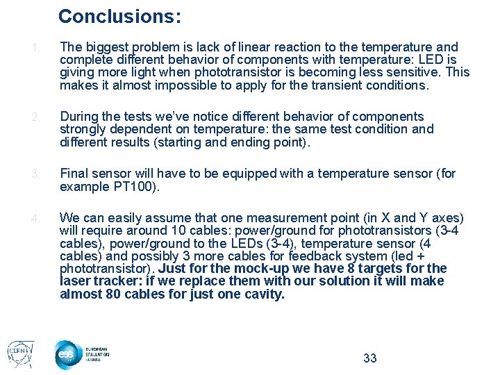
Conclusions: 1. The biggest problem is lack of linear reaction to the temperature and complete different behavior of components with temperature: LED is giving more light when phototransistor is becoming less sensitive. This makes it almost impossible to apply for the transient conditions. 2. During the tests we’ve notice different behavior of components strongly dependent on temperature: the same test condition and different results (starting and ending point). 3. Final sensor will have to be equipped with a temperature sensor (for example PT 100). 4. We can easily assume that one measurement point (in X and Y axes) will require around 10 cables: power/ground for phototransistors (3 -4 cables), power/ground to the LEDs (3 -4), temperature sensor (4 cables) and possibly 3 more cables for feedback system (led + phototransistor). Just for the mock-up we have 8 targets for the laser tracker: if we replace them with our solution it will make almost 80 cables for just one cavity. 33

Thank you for your attention! & Big „thank you”: to A. Vande Craen, K. Motala, M. Zapolski, M. Krupa, M. Strychalski, R. Bonnomi, M. Souchet, X. Sauvage, A. Guimet, A. Bastard, C. Petrone, J. G. Perez,
 Russian ballet terms
 A flexible loop of wire lies in a uniform magnetic field
 Why do magnets repel
 Wojciech korfanty
 Palenie sztandarów berezyna
 Wojciech dworakowski
 Ahtapol
 Wojciech sliwinski
 Silverlight 5 download
 Wojciech wencel
 Wojciech szpankowski
 Barbara adamiak
 Wojciech dworakowski
 Wojciech rodek
 Wstrząs janina
 Prof. wojciech krajewski
 Abstrakcjonizm malarze
 Wojciech lubas
 Ewald gawlik
 Wojciech krawczyk
 Kim był wojciech bartos
 Wojciech kic
 Jaboski
 Wojciech complak
 Wojciech duliński
 Niezawodność definicja
 Wojciech dadak uj
 Wojciech wyrzykowski pg
 Wojciech szpankowski
 Fundamental position
 Fundamental position vs anatomical position
 Maximum security fence
 Carbon fibre wire
 Difference between drawing and extrusion
 Ohno continuous cast copper wire

