Mrutyunjay Mjay University of Colorado Denver Hardware Trends
 University of Colorado, Denver")
 Huge main memory")


 is a specialized microprocessor for accelerating graphics rendering GPUs traditionally")


 Each SM has design of an")
 CMP:")


 GPU strengths are useful Memory bandwidth")


 is a data storage device that emulates a hard disk")


- Slides: 37
Mrutyunjay (Mjay) University of Colorado, Denver
Hardware Trends Multi-Core CPUs Many Core: Co-Processors GPU (NVIDIA, AMD Radeon) Huge main memory capacity with complex access characteristics (Caches, NUMA) Non-Volatile Storage Flash SSD (Solid State Drive)
Around 2005, frequencyscaling wall, improvements by adding multiple processing cores to the same CPU chip, forming chip multiprocessors servers with multiple CPU sockets of multicore processors (SMP of CMP)
Use Moore’s law to place more cores per chip 2 x cores/chip with each CMOS generation Roughly same clock frequency Known as multi-core chips or chip-multiprocessors (CMP) The good news Exponentially scaling peak performance No power problems due to clock frequency Easier design and verification The bad news Need parallel program if we want to ran a single app faster Power density is still an issue as transistors shrink
This how we think its works. This how EXACTLY it works.
Type of cores E. g. few OOO cores Vs many simple cores Memory hierarchy Which caching levels are shared and which are private Cache coherence Synchronization On-chip interconnect Bus Vs Ring Vs scalable interconnect (e. g. , mesh) Flat Vs hierarchical
All processor have access to unified physical memory The can communicate using loads and stores Advantages Looks like a better multithreaded processor (multitasking) Requires evolutionary changes the OS Threads within an app communicate implicitly without using OS Simpler to code for and low overhead App development: first focus on correctness, then on performance Disadvantages Implicit communication is hard to optimize Synchronization can get tricky Higher hardware complexity for cache management
NUMA: Non-Uniform Memory Access
GPU (Graphics Processing Unit) is a specialized microprocessor for accelerating graphics rendering GPUs traditionally for graphics computing GPUs now allow general purpose computing easily GPGPU: using GPU for general purpose computing Physics, Finance, Biology, Geosciences, Medicine, etc NVIDIA and AMD Radeon
GPU design with up to a thousand of core enables massively parallel computing GPUs architecture with streaming multiprocessors has form of SIMD processors CPU GPU
SIMD: Single Instruction Multiple Data Distributed memory SIMD computer Shared memory SIMD computer
Each GPU has ≥ 1 Streaming Multiprocessors (SMs) Each SM has design of an simple SIMD Processor 8 -192 Streaming Processors (SPs) NVIDIA Ge. Force 8 -Series GPUs and later
SMP of CMP: SMP: sockets of multicore processors (Multiple CPU in single system) CMP: Chip Multiprocessor (Single Chip with multi/many cores) SP: Streaming Processor SFU: Special Function Units Double Precision Unit Multithreaded Instruction Unit Hardware thread scheduling
14 Streaming Multiprocessors per GPU 32 cores per Streaming Multiprocessors
Two main approaches: Other tool ? Open. ACC
CUDA = Compute Unified Device Architecture A development framework for Nvidia GPUs Extensions of C language Support NVIDIA Ge. Force 8 -Series & later Host = CPU Device = GPU Host memory = RAM Device memory = RAM on GPU Host (CPU) Host memory PCI Express bus Device (GPU) Device memory
CPU sends data to the GPU CPU instructs the processing on GPU processes data CPU collects the results from GPU Host (CPU) 2 Host memory 1 4 Device (GPU) 3 Device memory
1. CPU sends data to the GPU Host Code int N= 1000; int size = N*sizeof(float); float A[1000], *d. A; 2. CPU instructs the processing on cuda. Malloc((void **)&d. A, size); cuda. Memcpy(d. A , A, size, GPU cuda. Memcpy. Host. To. Device); Compute. Array <<< 10, 20 >>> (d. A , N); 3. GPU processes data cuda. Memcpy(A, d. A, size, cuda. Memcpy. Device. To. Host); cuda. Free(d. A); Device Code __global__ void Compute. Array(float *A, int N) 4. CPU collects the results from GPU{ int i = block. Idx. x * block. Dim. x + thread. Idx. x; if (i<N) A[i] = A[i]*A[i]; }
• A kernel is executed as a grid of blocks • A block is a batch of threads that can cooperate with each other by: – Sharing data through shared memory – Synchronizing their execution • Threads from different blocks cannot cooperate
Limiting kernel launches Limiting data transfers(Solution Overlapped Transfers) GPU strengths are useful Memory bandwidth Parallel processing Accelerating SQL queries – 10 x improvement Also well suited for stream mining Continuous queries on streaming data instead of one-time queries on static database
Slowest part: Main Memory and Fixed Disk. Can we decrease the latency between Main Memory and Fixed disk? Solution: SSD
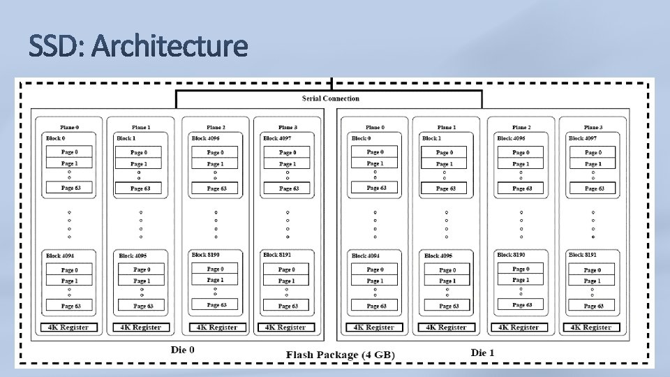
A Solid-State Disk (SSD) is a data storage device that emulates a hard disk drive (HDD). It has no moving parts like in HDD. NAND Flash SSD’s are essentially arrays of flash memory devices which include a controller that electrically and mechanically emulate, and are software compatible with magnetic HDD’s
Host Interface Logic SSD Controller RAM Buffer Flash Memory Package
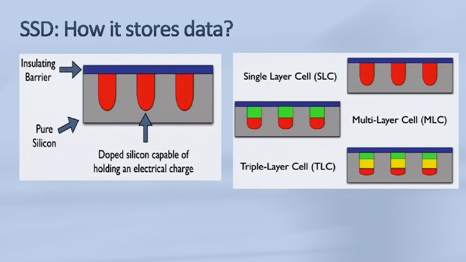
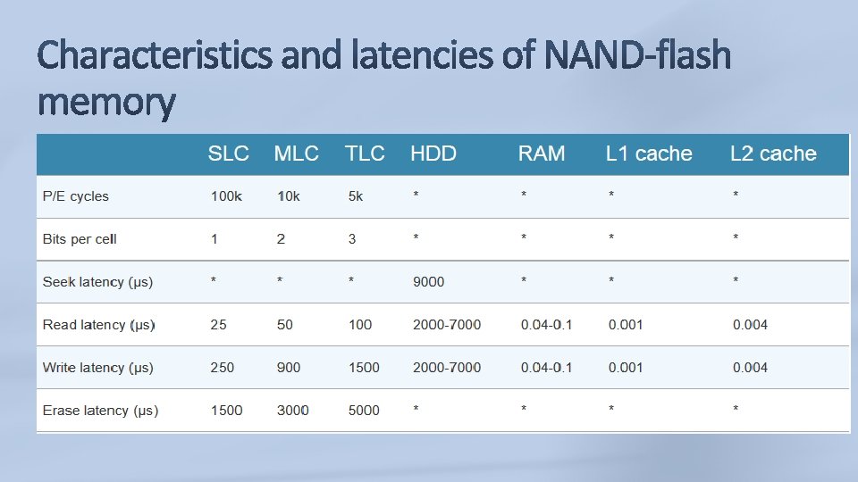
§ What will be the initial state of SSD? § NAND-flash cells have a limited lifespan due to their § Ans: Still looking for it. limited number of P/E cycles (Program/Erase Cycle)
Reads are aligned on page size: It is not possible to read less than one page at once. One can of course only request just one byte from the operating system, but a full page will be retrieved in the SSD, forcing a lot more data to be read than necessary. Writes are aligned on page size: When writing to an SSD, writes happen by increments of the page size. So even if a write operation affects only one byte, a whole page will be written anyway. Writing more data than necessary is known as write amplification Pages cannot be overwritten: A NAND-flash page can be written to only if it is in the “free” state. When data is changed, the content of the page is copied into an internal register, the data is updated, and the new version is stored in a “free” page, an operation called “read-modify-write”. Erases are aligned on block size: Pages cannot be overwritten, and once they become stale, the only way to make them free again is to erase them. However, it is not possible to erase individual pages, and it is only possible to erase whole blocks at once.
Align writes: Align writes on the page size, and write chunks of data that are multiple of the page size. Buffer small writes: To maximize throughput, whenever possible keep small writes into a buffer in RAM and when the buffer is full, perform a single large write to batch all the small writes
Latency difference for each type. More levels increases the latency: Delays in read and write. Solution: Hybrid SDD, consisting mixed levels
The garbage collection process in the SSD controller ensures that “stale” pages are erased and restored into a “free” state so that the incoming write commands can be processed. Split cold and hot data. : Hot data is data that changes frequently, and cold data is data that changes infrequently. If some hot data is stored in the same page as some cold data, the cold data will be copied along every time the hot data is updated in a read-modify-write operation, and will be moved along during garbage collection for wear leveling. Splitting cold and hot data as much as possible into separate pages will make the job of the garbage collector easier Buffer hot data: Extremely hot data should be buffered as much as possible and written to the drive as infrequently as possible.
The main factor that made adoption of SSDs so easy is that they use the same host interfaces as HDDs. Although presenting an array of Logical Block Addresses (LBA) makes sense for HDDs as their sectors can be overwritten, it is not fully suited to the way flash memory works For this reason, an additional component is required to hide the inner characteristics of NAND flash memory and expose only an array of LBAs to the host. This component is called the Flash Translation Layer (FTL), and resides in the SSD controller. The FTL is critical and has two main purposes: logical block mapping and garbage collection. This mapping takes the form of a table, which for any LBA gives the corresponding PBA. This mapping table is stored in the RAM of the SSD for speed of access, and is persisted in flash memory in case of power failure. When the SSD powers up, the table is read from the persisted version and reconstructed into the RAM of the SSD
Internal parallelism: Internally, several levels of parallelism allow to write to several blocks at once into different NANDflash chips, to what is called a “clustered block”. Multiple levels of parallelism: Channel-level parallelism Package-level parallelism Chip-level parallelism Plane-level parallelism
SSD Advantages Read and write are much faster than traditional HDD Allow PCs to boot up and launch programs far more quickly More physically Robust. Use less power and generate less heat SSD Disadvantages Lower capacity than HDDs Higher storage cost per GB Limited number of data write cycles Performance degradation over time
http: //codecapsule. com/2014/02/12/coding-for-ssds-part-6 -asummary-what-every-programmer-should-know-about-solidstate-drives/.