Module 6 Analogue Digital Converter C 28 x

- Slides: 21

Module 6 : Analogue Digital Converter C 28 x 32 -Bit-Digital Signal Controller TMS 320 F 2812 Texas Instruments Incorporated 6 -1

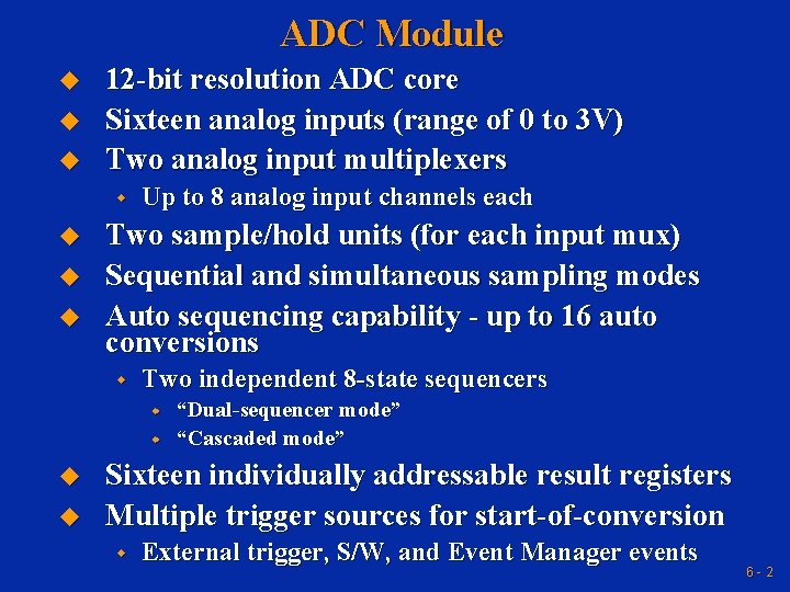
ADC Module u u u 12 -bit resolution ADC core Sixteen analog inputs (range of 0 to 3 V) Two analog input multiplexers w u u u Up to 8 analog input channels each Two sample/hold units (for each input mux) Sequential and simultaneous sampling modes Auto sequencing capability - up to 16 auto conversions w Two independent 8 -state sequencers w w u u “Dual-sequencer mode” “Cascaded mode” Sixteen individually addressable result registers Multiple trigger sources for start-of-conversion w External trigger, S/W, and Event Manager events 6 -2

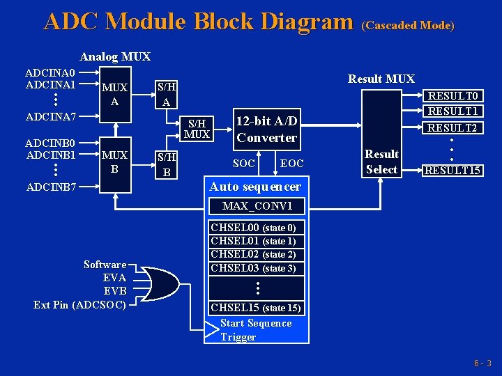
ADC Module Block Diagram (Cascaded Mode) Analog MUX . . . MUX A ADCINA 7 ADCINB 0 ADCINB 1 Result MUX S/H A S/H MUX . . . MUX B ADCINB 7 S/H B RESULT 0 RESULT 1 RESULT 2 12 -bit A/D Converter SOC EOC Result Select . . . ADCINA 0 ADCINA 1 RESULT 15 Auto sequencer MAX_CONV 1 . . . Software EVA EVB Ext Pin (ADCSOC) CHSEL 00 (state 0) CHSEL 01 (state 1) CHSEL 02 (state 2) CHSEL 03 (state 3) CHSEL 15 (state 15) Start Sequence Trigger 6 -3

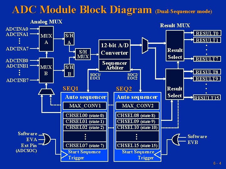
ADC Module Block Diagram (Dual-Sequencer mode) Analog MUX S/H A ADCINA 7 ADCINB 0 ADCINB 1 . . . ADCINB 7 SOC 1/ EOC 1 SEQ 1 Auto sequencer SEQ 2 Auto sequencer MAX_CONV 1 MAX_CONV 2 CHSEL 00 (state 0) CHSEL 01 (state 1) CHSEL 02 (state 2) CHSEL 08 (state 8) CHSEL 09 (state 9) CHSEL 10 (state 10) CHSEL 07 (state 7) Start Sequence Trigger CHSEL 15 (state 15) Start Sequence Trigger RESULT 7 RESULT 8 RESULT 9 SOC 2/ EOC 2 . . . (ADCSOC) S/H B Result Select Sequencer Arbiter . . . Software EVA Ext Pin 12 -bit A/D Converter S/H MUX B RESULT 0 RESULT 1 . . . MUX A Result MUX Result Select . . . ADCINA 0 ADCINA 1 RESULT 15 Software EVB 6 -4

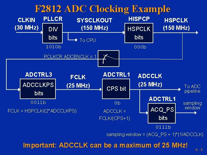
F 2812 ADC Clocking Example CLKIN PLLCR (30 MHz) DIV bits HISPCP SYSCLKOUT (150 MHz) HSPCLK bits To CPU 1010 b 000 b PCLKCR. ADCENCLK = 1 ADCTRL 3 ADCCLKPS bits FCLK (25 MHz) 0011 b FCLK = HSPCLK/(2*ADCCLKPS) ADCTRL 1 CPS bit 0 b ADCCLK = FCLK/(CPS+1) ADCCLK (25 MHz) ADCTRL 1 ACQ_PS bits To ADC pipeline sampling window 0111 b sampling window = (ACQ_PS + 1)*(1/ADCCLK) Important: ADCCLK can be a maximum of 25 MHz! 6 -5

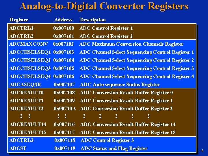
Analog-to-Digital Converter Registers Register Address Description ADCTRL 1 0 x 007100 ADC Control Register 1 ADCTRL 2 0 x 007101 ADC Control Register 2 ADCMAXCONV 0 x 007102 ADC Maximum Conversion Channels Register ADCCHSELSEQ 1 0 x 007103 ADC Channel Select Sequencing Control Register 1 ADCCHSELSEQ 2 0 x 007104 ADC Channel Select Sequencing Control Register 2 ADCCHSELSEQ 3 0 x 007105 ADC Channel Select Sequencing Control Register 3 ADCCHSELSEQ 4 0 x 007106 ADC Channel Select Sequencing Control Register 4 ADCASEQSR 0 x 007107 ADC Auto sequence Status Register ADCRESULT 0 0 x 007108 ADC Conversion Result Buffer Register 0 ADCRESULT 1 0 x 007109 ADC Conversion Result Buffer Register 1 ADCRESULT 2 0 x 00710 A ADC Conversion Result Buffer Register 2 ADCRESULT 14 0 x 007116 ADC Conversion Result Buffer Register 14 ADCRESULT 15 0 x 007117 ADC Conversion Result Buffer Register 15 ADCTRL 3 0 x 007118 ADC Control Register 3 ADCST 0 x 007119 ADC Status and Flag Register : : : 6 -6

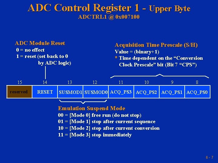
ADC Control Register 1 - Upper Byte ADCTRL 1 @ 0 x 007100 ADC Module Reset Acquisition Time Prescale (S/H) 0 = no effect 1 = reset (set back to 0 by ADC logic) 15 14 reserved RESET 13 Value = (binary+1) * Time dependent on the “Conversion Clock Prescale” bit (Bit 7 “CPS”) 12 11 10 9 8 SUSMOD 1 SUSMOD 0 ACQ_PS 3 ACQ_PS 2 ACQ_PS 1 ACQ_PS 0 Emulation Suspend Mode 00 = [Mode 0] free run (do not stop) 01 = [Mode 1] stop after current sequence 10 = [Mode 2] stop after current conversion 11 = [Mode 3] stop immediately 6 -7

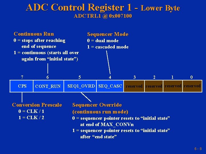
ADC Control Register 1 - Lower Byte ADCTRL 1 @ 0 x 007100 Continuous Run 0 = stops after reaching end of sequence 1 = continuous (starts all over again from “initial state”) 7 6 CPS CONT_RUN Conversion Prescale 0 = CLK / 1 1 = CLK / 2 5 Sequencer Mode 0 = dual mode 1 = cascaded mode 4 3 2 1 0 SEQ 1_OVRD SEQ_CASC reserved Sequencer Override (continuous run mode) 0 = sequencer pointer resets to “initial state” at end of MAX_CONVn 1 = sequencer pointer resets to “initial state” after “end state” 6 -8

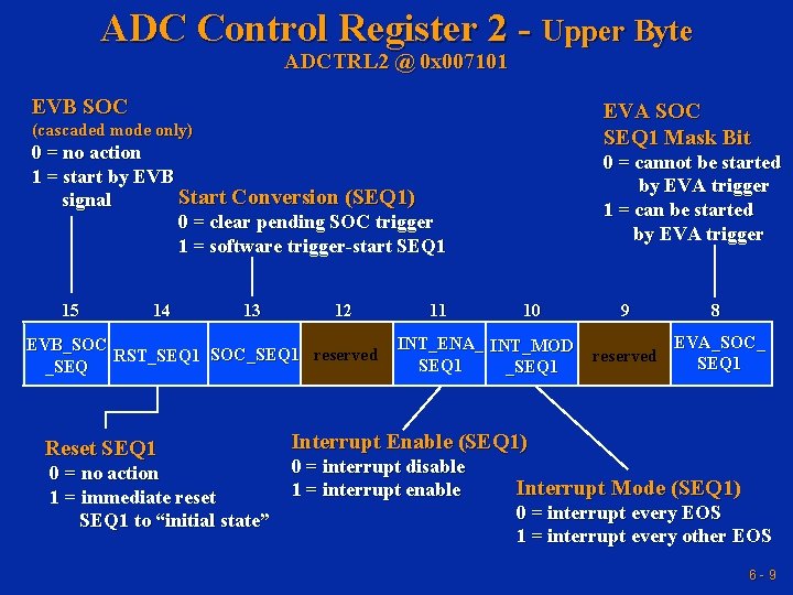
ADC Control Register 2 - Upper Byte ADCTRL 2 @ 0 x 007101 EVB SOC EVA SOC SEQ 1 Mask Bit (cascaded mode only) 0 = no action 1 = start by EVB Start Conversion (SEQ 1) signal 0 = clear pending SOC trigger 1 = software trigger-start SEQ 1 15 14 13 12 EVB_SOC RST_SEQ 1 SOC_SEQ 1 reserved _SEQ Reset SEQ 1 0 = no action 1 = immediate reset SEQ 1 to “initial state” 11 0 = cannot be started by EVA trigger 1 = can be started by EVA trigger 10 INT_ENA_ INT_MOD SEQ 1 _SEQ 1 9 8 reserved EVA_SOC_ SEQ 1 Interrupt Enable (SEQ 1) 0 = interrupt disable 1 = interrupt enable Interrupt Mode (SEQ 1) 0 = interrupt every EOS 1 = interrupt every other EOS 6 -9

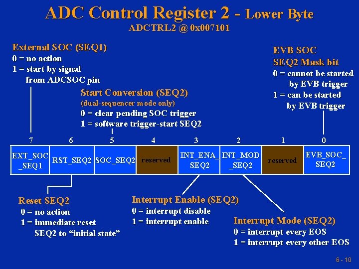
ADC Control Register 2 - Lower Byte ADCTRL 2 @ 0 x 007101 External SOC (SEQ 1) EVB SOC SEQ 2 Mask bit 0 = no action 1 = start by signal from ADCSOC pin 0 = cannot be started by EVB trigger 1 = can be started by EVB trigger Start Conversion (SEQ 2) (dual-sequencer mode only) 0 = clear pending SOC trigger 1 = software trigger-start SEQ 2 7 6 5 4 EXT_SOC RST_SEQ 2 SOC_SEQ 2 reserved _SEQ 1 Reset SEQ 2 0 = no action 1 = immediate reset SEQ 2 to “initial state” 3 2 INT_ENA_ INT_MOD SEQ 2 _SEQ 2 1 0 reserved EVB_SOC_ SEQ 2 Interrupt Enable (SEQ 2) 0 = interrupt disable 1 = interrupt enable Interrupt Mode (SEQ 2) 0 = interrupt every EOS 1 = interrupt every other EOS 6 - 10

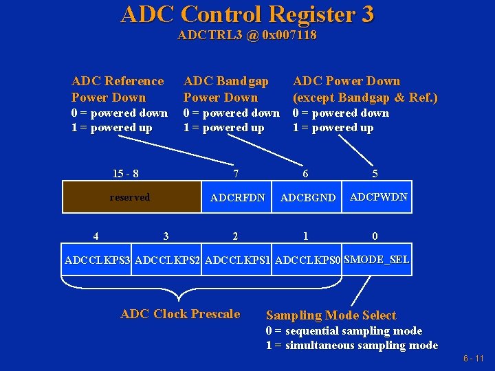
ADC Control Register 3 ADCTRL 3 @ 0 x 007118 ADC Reference Power Down ADC Bandgap Power Down 0 = powered down 1 = powered up 15 - 8 reserved 4 3 ADC Power Down (except Bandgap & Ref. ) 7 6 5 ADCRFDN ADCBGND ADCPWDN 2 1 0 ADCCLKPS 3 ADCCLKPS 2 ADCCLKPS 1 ADCCLKPS 0 SMODE_SEL ADC Clock Prescale Sampling Mode Select 0 = sequential sampling mode 1 = simultaneous sampling mode 6 - 11

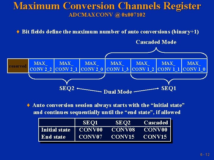
Maximum Conversion Channels Register ADCMAXCONV @ 0 x 007102 ¨ Bit fields define the maximum number of auto conversions (binary+1) Cascaded Mode reserved MAX_ MAX_ CONV 2_2 CONV 2_1 CONV 2_0 CONV 1_3 CONV 1_2 CONV 1_1 CONV 1_0 SEQ 2 Dual Mode SEQ 1 ¨ Auto conversion session always starts with the “initial state” and continues sequentially until the “end state”, if allowed Initial state End state SEQ 1 CONV 00 CONV 07 SEQ 2 CONV 08 CONV 15 Cascaded CONV 00 CONV 15 6 - 12

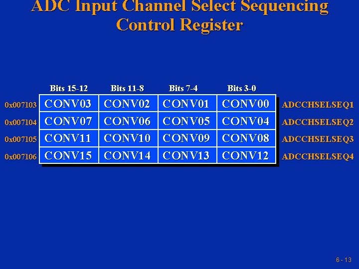
ADC Input Channel Select Sequencing Control Register 0 x 007103 0 x 007104 0 x 007105 0 x 007106 Bits 15 -12 Bits 11 -8 CONV 03 CONV 07 CONV 11 CONV 15 CONV 02 CONV 06 CONV 10 CONV 14 Bits 7 -4 CONV 01 CONV 05 CONV 09 CONV 13 Bits 3 -0 CONV 04 CONV 08 CONV 12 ADCCHSELSEQ 1 ADCCHSELSEQ 2 ADCCHSELSEQ 3 ADCCHSELSEQ 4 6 - 13

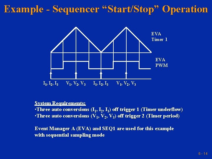
Example - Sequencer “Start/Stop” Operation EVA Timer 1 EVA PWM I 1, I 2, I 3 V 1, V 2, V 3 System Requirements: • Three auto conversions (I 1, I 2, I 3) off trigger 1 (Timer underflow) • Three auto conversions (V 1, V 2, V 3) off trigger 2 (Timer period) Event Manager A (EVA) and SEQ 1 are used for this example with sequential sampling mode 6 - 14

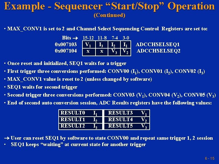
Example - Sequencer “Start/Stop” Operation (Continued) • MAX_CONV 1 is set to 2 and Channel Select Sequencing Control Registers are set to: Bits 15 -12 11 -8 0 x 007103 V 1 I 3 0 x 007104 x x 7 -4 3 -0 I 2 I 1 V 3 V 2 ADCCHSELSEQ 1 ADCCHSELSEQ 2 • Once reset and initialized, SEQ 1 waits for a trigger • First trigger three conversions performed: CONV 00 (I 1), CONV 01 (I 2), CONV 02 (I 3) • MAX_CONV 1 value is reset to 2 (unless changed by software) • SEQ 1 waits for second trigger • Second trigger three conversions performed: CONV 03 (V 1), CONV 04 (V 2), CONV 05 (V 3) • End of second auto conversion session, ADC Results registers have the following values: RESULT 0 RESULT 1 RESULT 2 I 1 I 2 I 3 RESULT 4 RESULT 5 V 1 V 2 V 3 User can reset SEQ 1 by software to state CONV 00 and repeat same trigger 1, 2 session • SEQ 1 keeps “waiting” at current state for another trigger 6 - 15

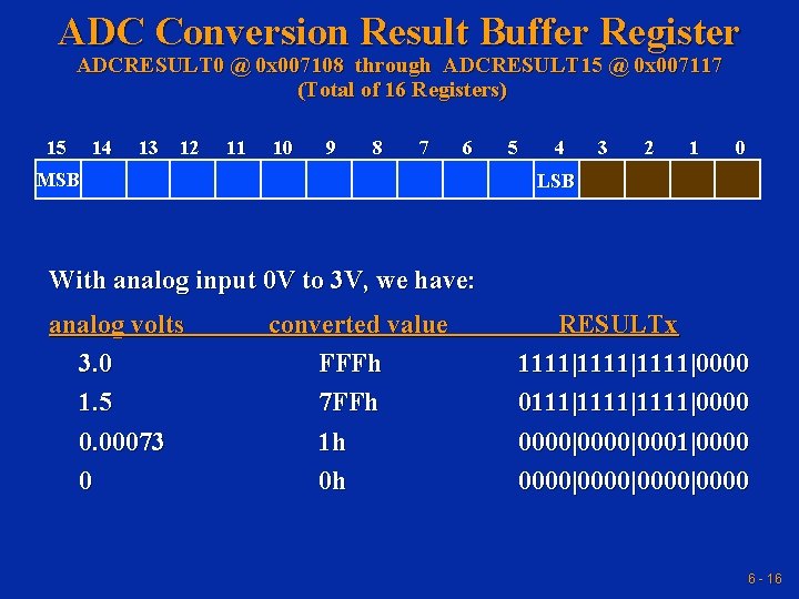
ADC Conversion Result Buffer Register ADCRESULT 0 @ 0 x 007108 through ADCRESULT 15 @ 0 x 007117 (Total of 16 Registers) 15 14 13 12 11 10 9 8 7 6 MSB 5 4 3 2 1 0 LSB With analog input 0 V to 3 V, we have: analog volts 3. 0 1. 5 0. 00073 0 converted value FFFh 7 FFh 1 h 0 h RESULTx 1111|1111|0000 0111|1111|0000|0000|0000|0000 6 - 16

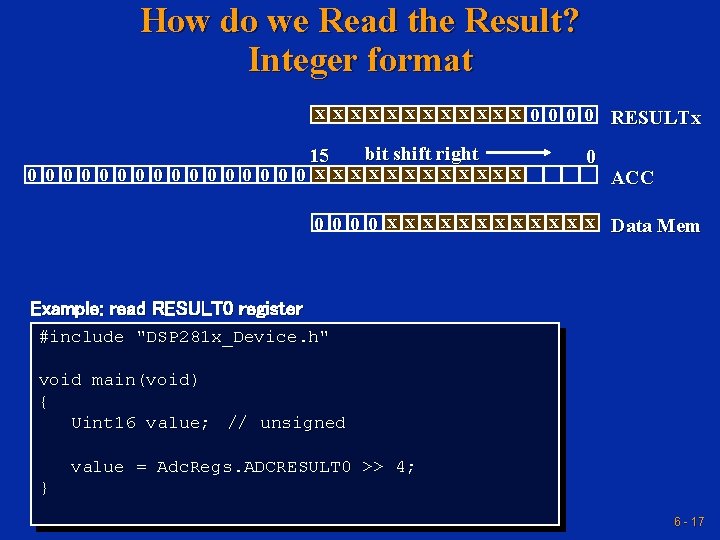
How do we Read the Result? Integer format x x x 0 0 RESULTx bit shift right 15 0 0 0 0 x x x x xx x 0 ACC 0 0 x x x Data Mem Example: read RESULT 0 register #include "DSP 281 x_Device. h" void main(void) { Uint 16 value; // unsigned value = Adc. Regs. ADCRESULT 0 >> 4; } 6 - 17

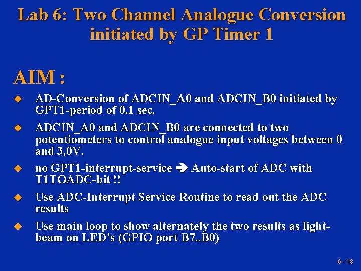
Lab 6: Two Channel Analogue Conversion initiated by GP Timer 1 AIM : u u u AD-Conversion of ADCIN_A 0 and ADCIN_B 0 initiated by GPT 1 -period of 0. 1 sec. ADCIN_A 0 and ADCIN_B 0 are connected to two potentiometers to control analogue input voltages between 0 and 3, 0 V. no GPT 1 -interrupt-service Auto-start of ADC with T 1 TOADC-bit !! Use ADC-Interrupt Service Routine to read out the ADC results Use main loop to show alternately the two results as lightbeam on LED’s (GPIO port B 7. . B 0) 6 - 18

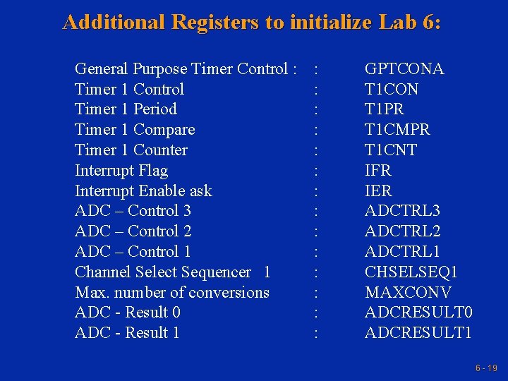
Additional Registers to initialize Lab 6: General Purpose Timer Control : Timer 1 Control Timer 1 Period Timer 1 Compare Timer 1 Counter Interrupt Flag Interrupt Enable ask ADC – Control 3 ADC – Control 2 ADC – Control 1 Channel Select Sequencer 1 Max. number of conversions ADC - Result 0 ADC - Result 1 : : : : GPTCONA T 1 CON T 1 PR T 1 CMPR T 1 CNT IFR IER ADCTRL 3 ADCTRL 2 ADCTRL 1 CHSELSEQ 1 MAXCONV ADCRESULT 0 ADCRESULT 1 6 - 19

Optional Lab 6 A Modify Lab-Exercise 4 ( ‘Knight-Rider’) : • use the Analogue Input ADCIN 0 to change the frequency for the LED’s • to add the ADC-setup use Lab 6 as a start • use a LED-frequency range between 50 Hz and 1 Hz • use (1) a linear or (2) a logarithm scale between Fmin and Fmax. 6 - 20
