
DNT 125 ANALOGUE ELECTRONICS Chapter 3 Bipolar Junction
DNT 125 ANALOGUE ELECTRONICS Chapter 3 Bipolar Junction Transistors (BJT) Pn Maizatul Nurul Bariah Binti Ahmad E-mail: maizatulnurul@unimap. edu. my Phone : 019 -4052335 1

BJT Structure BJT- Basic Construction • BJT is constructed with 3 doped semiconductor regions separated by 2 pn junctions (Base-Collector & Base-Emitter). • 3 regions are called emitter, base and collector. o Emitter (E) – most heavily doped region. o Base (B) – thin and lightly doped region. 2 o Collector (C) – largest and moderately doped region.

BJT Structure BJT- Standard Symbols 3

BJT Operation In order for a BJT to operate as amplifier, the two pn junctions must be correctly biased with external dc voltages. The operation of pnp is the same as npn except that the roles of electrons and holes, the bias voltage polarities and the current directions are all reversed. Figure below shows the bias arrangement for npn and pnp to operate as an amplifier. In normal operation, the base-emitter is forward-biased while the base-collector is reverse-biased. This condition is called forward-reverse bias 4
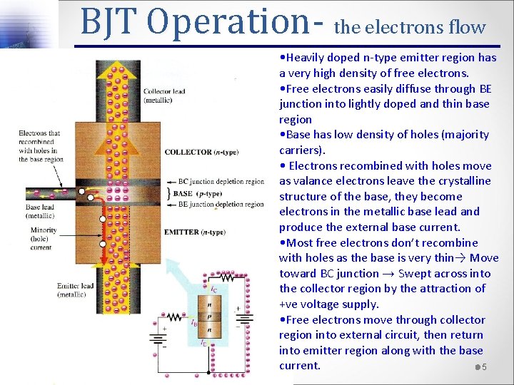
BJT Operation- the electrons flow • Heavily doped n-type emitter region has a very high density of free electrons. • Free electrons easily diffuse through BE junction into lightly doped and thin base region • Base has low density of holes (majority carriers). • Electrons recombined with holes move as valance electrons leave the crystalline structure of the base, they become electrons in the metallic base lead and produce the external base current. • Most free electrons don’t recombine with holes as the base is very thin→ Move toward BC junction → Swept across into the collector region by the attraction of +ve voltage supply. • Free electrons move through collector region into external circuit, then return into emitter region along with the base current. 5
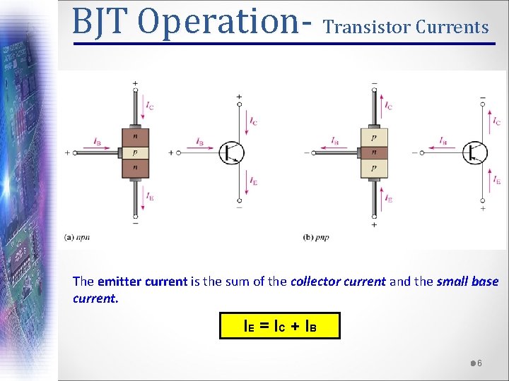
BJT Operation- Transistor Currents The emitter current is the sum of the collector current and the small base current. IE = I C + I B 6
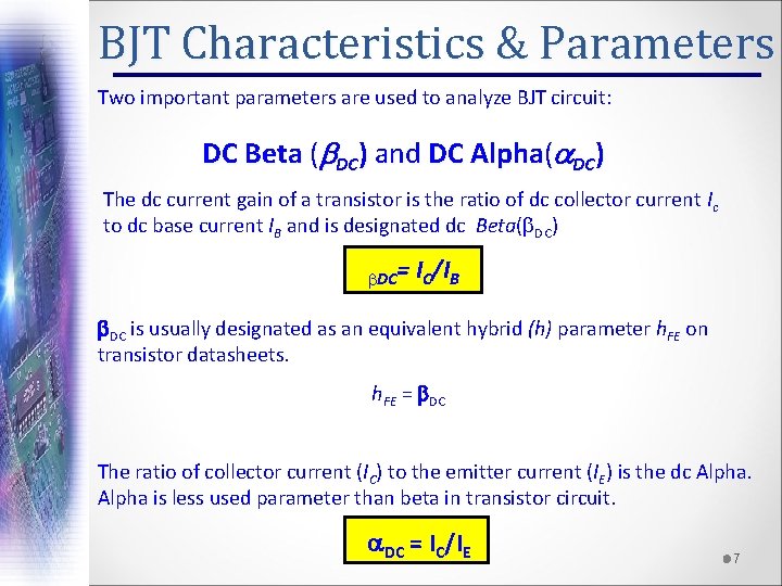
BJT Characteristics & Parameters Two important parameters are used to analyze BJT circuit: DC Beta ( DC) and DC Alpha( DC) The dc current gain of a transistor is the ratio of dc collector current Ic to dc base current IB and is designated dc Beta( DC) DC= IC/IB DC is usually designated as an equivalent hybrid (h) parameter h. FE on transistor datasheets. h. FE = DC The ratio of collector current (IC) to the emitter current (IE) is the dc Alpha is less used parameter than beta in transistor circuit. DC = IC/IE 7
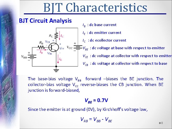
BJT Characteristics BJT Circuit Analysis IB : dc base current IE : dc emitter current IC : dc ecollector current VBE : dc voltage at base with respect to emitter VCE : dc voltage at collector with respect to emitter VCB : dc voltage at collector with respect to base The base-bias voltage VBB forward –biases the BE junction. The collector-bias voltage VCC reverse-biases the CB junction. When BE junction is forward-biased, VBE ≈ 0. 7 V Since the emitter is at ground (0 V), by Kirchhoff's voltage law, VRB = VBB - VBE 8
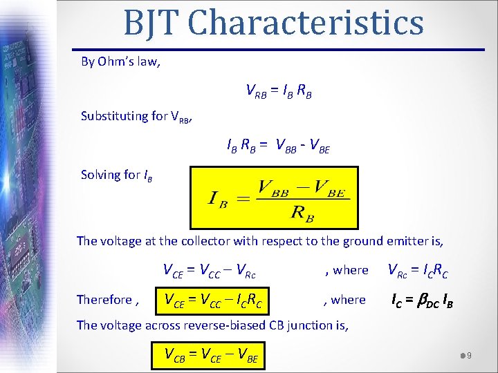
BJT Characteristics By Ohm’s law, VRB = IB RB Substituting for VRB, IB RB = VBB - VBE Solving for IB The voltage at the collector with respect to the ground emitter is, Therefore , VCE = VCC – VRc , where VRc = ICRC VCE = VCC – ICRC , where IC = DC IB The voltage across reverse-biased CB junction is, VCB = VCE – VBE 9
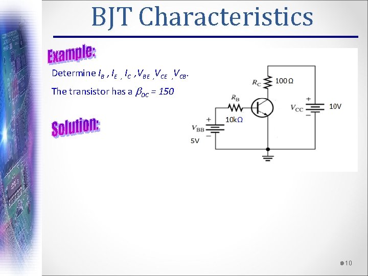
BJT Characteristics Determine IB , IE , IC , VBE , VCB. The transistor has a DC = 150 10
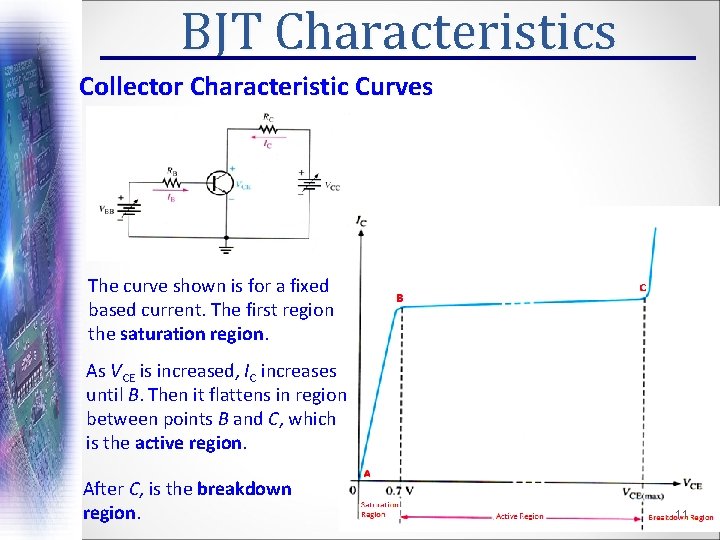
BJT Characteristics Collector Characteristic Curves The curve shown is for a fixed based current. The first region is the saturation region. As VCE is increased, IC increases until B. Then it flattens in region between points B and C, which is the active region. After C, is the breakdown region. 11
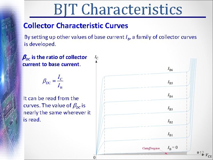
BJT Characteristics Collector Characteristic Curves By setting up other values of base current IB, a family of collector curves is developed. DC is the ratio of collector current to base current. It can be read from the curves. The value of DC is nearly the same wherever it is read. 12
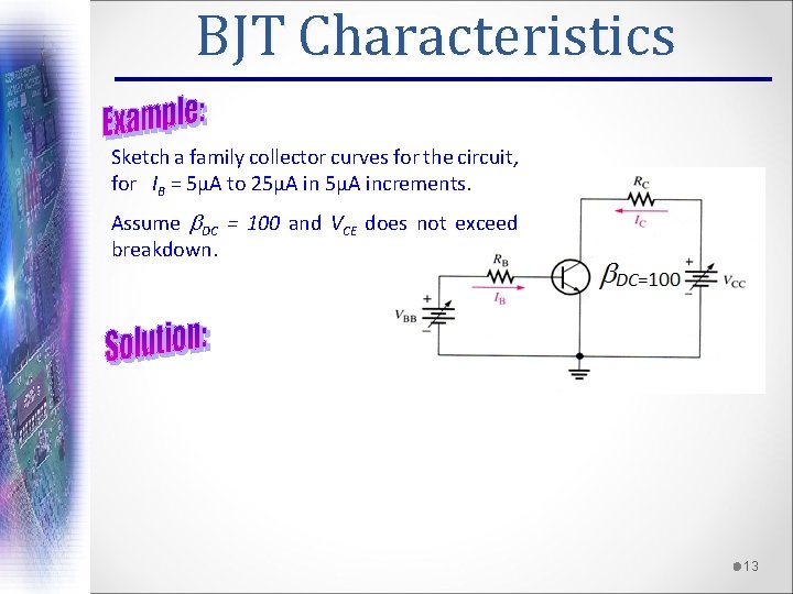
BJT Characteristics Sketch a family collector curves for the circuit, for IB = 5µA to 25µA increments. Assume DC = 100 and VCE does not exceed breakdown. 13
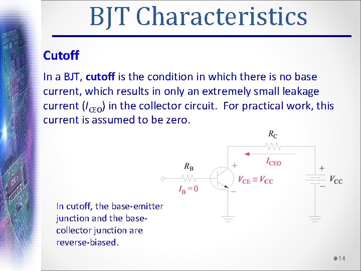
BJT Characteristics Cutoff In a BJT, cutoff is the condition in which there is no base current, which results in only an extremely small leakage current (ICEO) in the collector circuit. For practical work, this current is assumed to be zero. In cutoff, the base-emitter junction and the basecollector junction are reverse-biased. 14
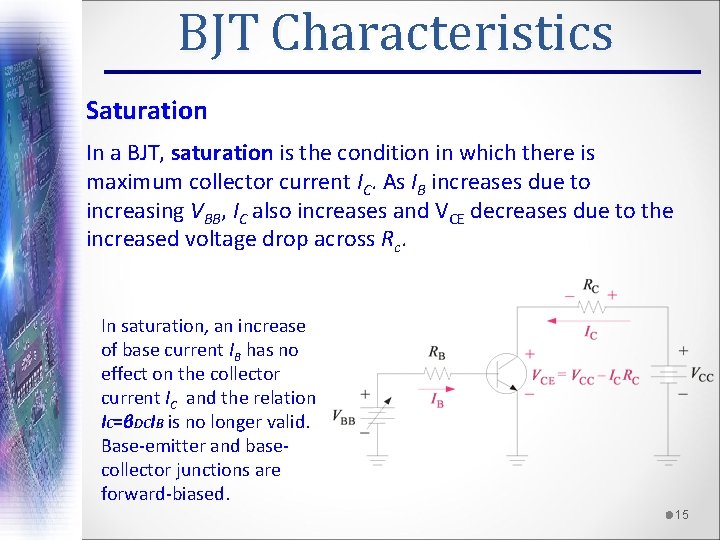
BJT Characteristics Saturation In a BJT, saturation is the condition in which there is maximum collector current IC. As IB increases due to increasing VBB, IC also increases and VCE decreases due to the increased voltage drop across Rc. In saturation, an increase of base current IB has no effect on the collector current IC and the relation IC=βDCIB is no longer valid. Base-emitter and basecollector junctions are forward-biased. 15
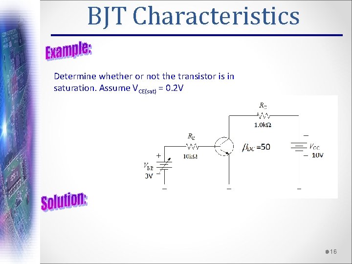
BJT Characteristics Determine whether or not the transistor is in saturation. Assume VCE(sat) = 0. 2 V 16
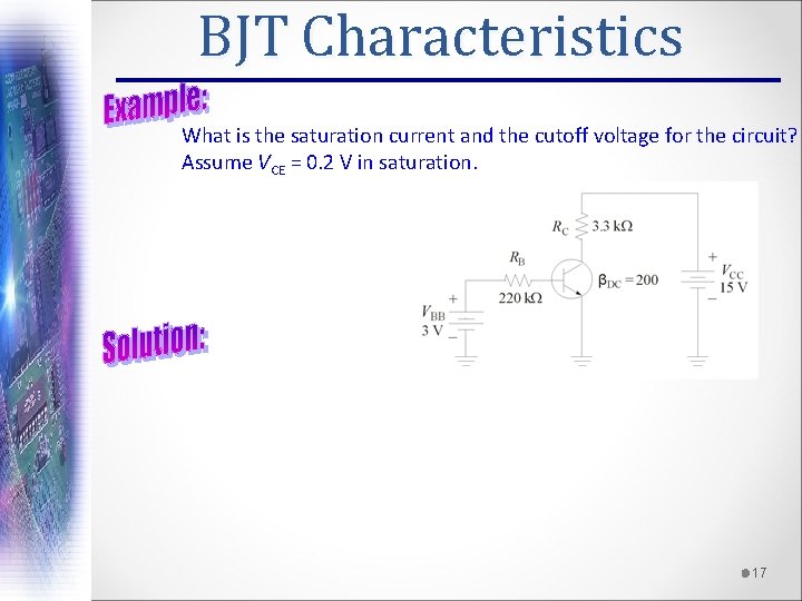
BJT Characteristics What is the saturation current and the cutoff voltage for the circuit? Assume VCE = 0. 2 V in saturation. 17
- Slides: 17