Modeling microchannel plate detectors for improved performance Romualdo

- Slides: 32

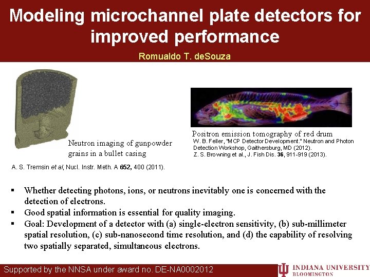
Modeling microchannel plate detectors for improved performance Romualdo T. de. Souza Positron emission tomography of red drum Neutron imaging of gunpowder grains in a bullet casing W. B. Feller, “MCP Detector Development. ” Neutron and Photon Detection Workshop, Gaithersburg, MD (2012). Z. S. Browning et al. , J. Fish Dis. 36, 911 -919 (2013). A. S. Tremsin et al, Nucl. Instr. Meth. A 652, 400 (2011). § § § Whether detecting photons, ions, or neutrons inevitably one is concerned with the detection of electrons. Good spatial information is essential for quality imaging. Goal: Development of a detector with (a) single-electron sensitivity, (b) sub-millimeter spatial resolution, (c) sub-nanosecond time resolution, and (d) the capability of resolving two spatially separated, simultaneous electrons. Supported by the NNSA under award no. DE-NA 0002012

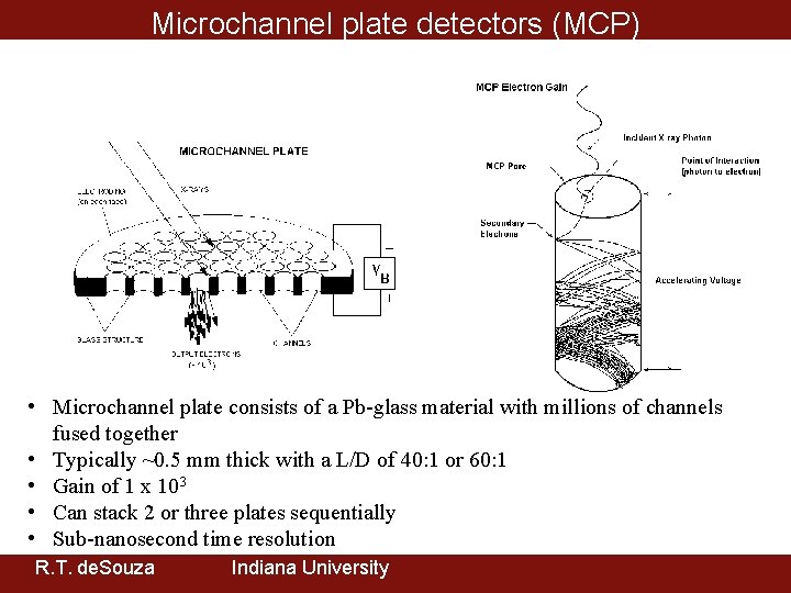
Microchannel plate detectors (MCP) • Microchannel plate consists of a Pb-glass material with millions of channels fused together • Typically ~0. 5 mm thick with a L/D of 40: 1 or 60: 1 • Gain of 1 x 10³ • Can stack 2 or three plates sequentially • Sub-nanosecond time resolution R. T. de. Souza Indiana University

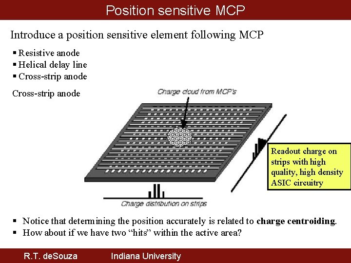
Position sensitive MCP Introduce a position sensitive element following MCP § Resistive anode § Helical delay line § Cross-strip anode Readout charge on strips with high quality, high density ASIC circuitry § Notice that determining the position accurately is related to charge centroiding. § How about if we have two “hits” within the active area? R. T. de. Souza Indiana University

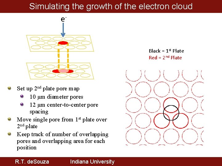
Simulating the growth of the electron cloud e. Plate 1 Black = 1 st Plate Red = 2 nd Plate 2 Set up 2 nd plate pore map 10 μm diameter pores 12 μm center-to-center pore spacing Move single pore from 1 st plate over 2 nd plate Keep track of number of overlapping pores and overlapping area for each position R. T. de. Souza Indiana University

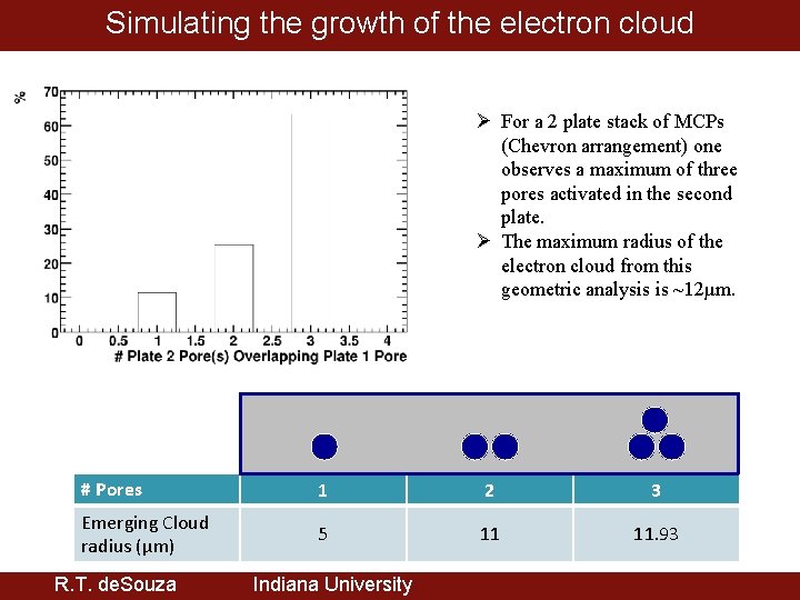
Simulating the growth of the electron cloud Ø For a 2 plate stack of MCPs (Chevron arrangement) one observes a maximum of three pores activated in the second plate. Ø The maximum radius of the electron cloud from this geometric analysis is ~12µm. # Pores 1 2 3 Emerging Cloud radius (μm) 5 11 11. 93 R. T. de. Souza Indiana University

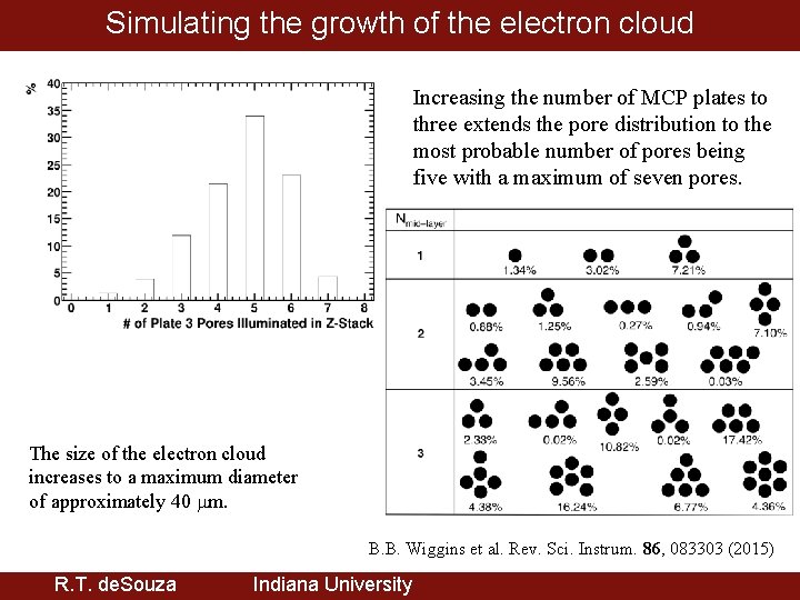
Simulating the growth of the electron cloud Increasing the number of MCP plates to three extends the pore distribution to the most probable number of pores being five with a maximum of seven pores. The size of the electron cloud increases to a maximum diameter of approximately 40 m. B. B. Wiggins et al. Rev. Sci. Instrum. 86, 083303 (2015) R. T. de. Souza Indiana University

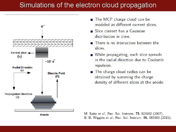
Simulations of the electron cloud propagation

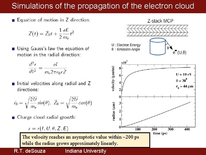
Simulations of the propagation of the electron cloud The velocity reaches an asymptotic value within ~200 ps while the radius grows approximately linearly. R. T. de. Souza Indiana University

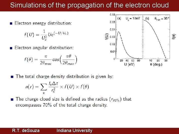
Simulations of the propagation of the electron cloud R. T. de. Souza Indiana University

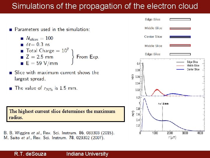
Simulations of the propagation of the electron cloud The highest current slice determines the maximum radius. R. T. de. Souza Indiana University

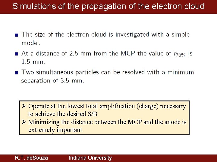
Simulations of the propagation of the electron cloud Ø Operate at the lowest total amplification (charge) necessary to achieve the desired S/B Ø Minimizing the distance between the MCP and the anode is extremely important R. T. de. Souza Indiana University

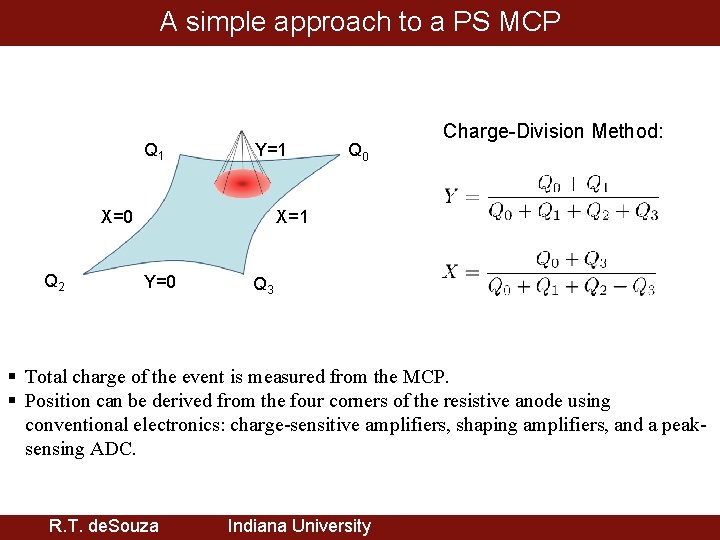
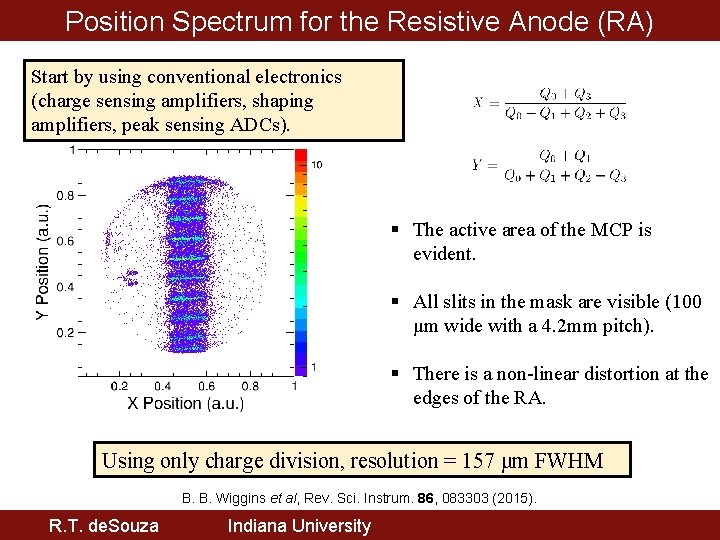
A simple approach to a PS MCP Q 1 Y=1 X=0 Q 2 Q 0 Charge-Division Method: X=1 Y=0 Q 3 § Total charge of the event is measured from the MCP. § Position can be derived from the four corners of the resistive anode using conventional electronics: charge-sensitive amplifiers, shaping amplifiers, and a peaksensing ADC. R. T. de. Souza Indiana University

Position Spectrum for the Resistive Anode (RA) Start by using conventional electronics (charge sensing amplifiers, shaping amplifiers, peak sensing ADCs). § The active area of the MCP is evident. § All slits in the mask are visible (100 μm wide with a 4. 2 mm pitch). § There is a non-linear distortion at the edges of the RA. Using only charge division, resolution = 157 μm FWHM B. B. Wiggins et al, Rev. Sci. Instrum. 86, 083303 (2015). R. T. de. Souza Indiana University

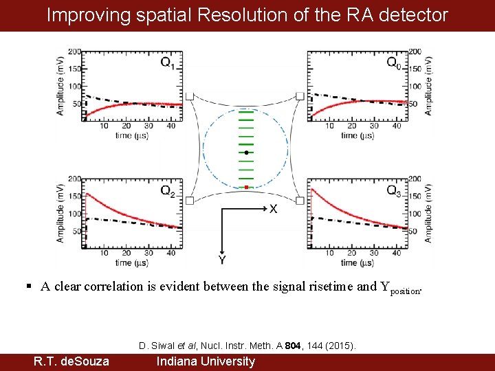
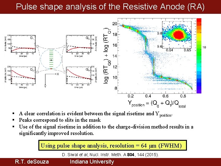
Improving spatial Resolution of the RA detector § A clear correlation is evident between the signal risetime and Yposition. D. Siwal et al, Nucl. Instr. Meth. A 804, 144 (2015). R. T. de. Souza Indiana University

Pulse shape analysis of the Resistive Anode (RA) § A clear correlation is evident between the signal risetime and Yposition. § Peaks correspond to slits in the mask § Use of the signal risetime in addition to the charge-division method results in a significantly improved resolution. Using pulse shape analysis, resolution = 64 μm (FWHM) D. Siwal et al, Nucl. Instr. Meth. A 804, 144 (2015). R. T. de. Souza Indiana University

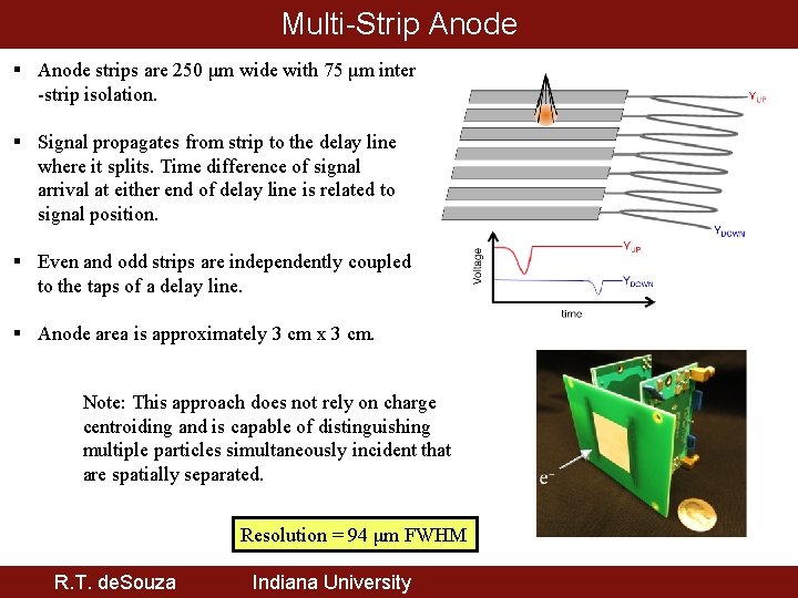
Multi-Strip Anode § Anode strips are 250 μm wide with 75 μm inter -strip isolation. § Signal propagates from strip to the delay line where it splits. Time difference of signal arrival at either end of delay line is related to signal position. § Even and odd strips are independently coupled to the taps of a delay line. § Anode area is approximately 3 cm x 3 cm. Note: This approach does not rely on charge centroiding and is capable of distinguishing multiple particles simultaneously incident that are spatially separated. Resolution = 94 μm FWHM R. T. de. Souza Indiana University

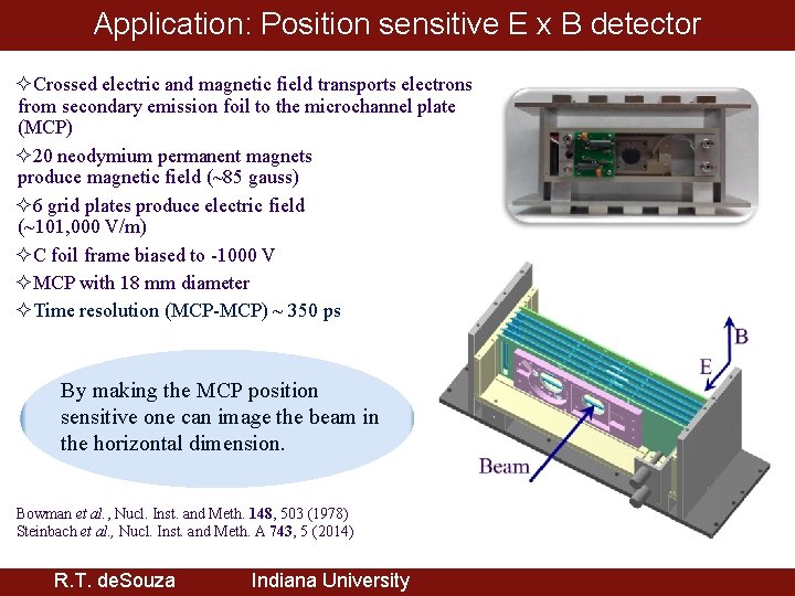
Application: Position sensitive E x B detector ²Crossed electric and magnetic field transports electrons from secondary emission foil to the microchannel plate (MCP) ² 20 neodymium permanent magnets produce magnetic field (~85 gauss) ² 6 grid plates produce electric field (~101, 000 V/m) ²C foil frame biased to -1000 V ²MCP with 18 mm diameter ²Time resolution (MCP-MCP) ~ 350 ps By making the MCP position sensitive one can image the beam in the horizontal dimension. Bowman et al. , Nucl. Inst. and Meth. 148, 503 (1978) Steinbach et al. , Nucl. Inst. and Meth. A 743, 5 (2014) R. T. de. Souza Indiana University

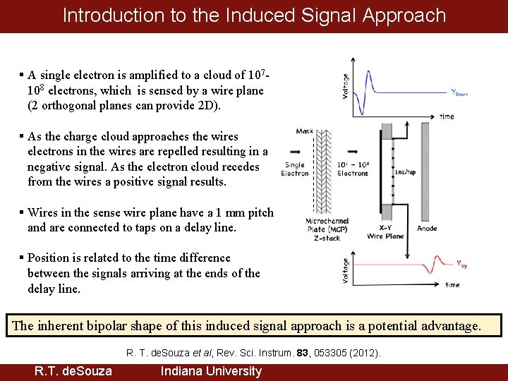
Introduction to the Induced Signal Approach § A single electron is amplified to a cloud of 107108 electrons, which is sensed by a wire plane (2 orthogonal planes can provide 2 D). § As the charge cloud approaches the wires electrons in the wires are repelled resulting in a negative signal. As the electron cloud recedes from the wires a positive signal results. § Wires in the sense wire plane have a 1 mm pitch and are connected to taps on a delay line. § Position is related to the time difference between the signals arriving at the ends of the delay line. The inherent bipolar shape of this induced signal approach is a potential advantage. R. T. de. Souza et al, Rev. Sci. Instrum. 83, 053305 (2012). R. T. de. Souza Indiana University

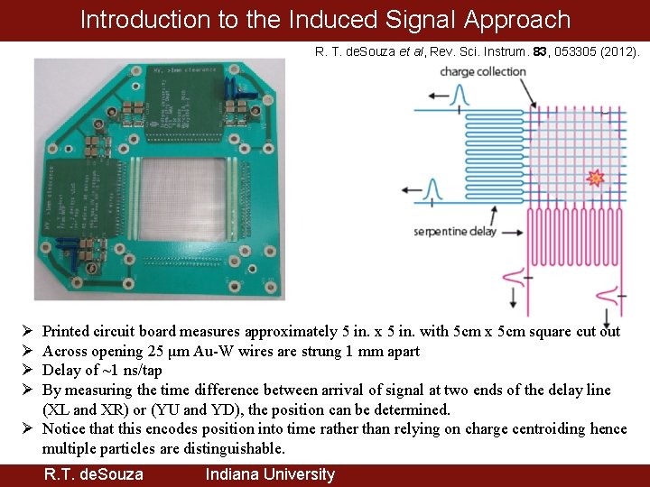
Introduction to the Induced Signal Approach R. T. de. Souza et al, Rev. Sci. Instrum. 83, 053305 (2012). Ø Ø Printed circuit board measures approximately 5 in. x 5 in. with 5 cm x 5 cm square cut out Across opening 25 μm Au-W wires are strung 1 mm apart Delay of ~1 ns/tap By measuring the time difference between arrival of signal at two ends of the delay line (XL and XR) or (YU and YD), the position can be determined. Ø Notice that this encodes position into time rather than relying on charge centroiding hence multiple particles are distinguishable. R. T. de. Souza Indiana University

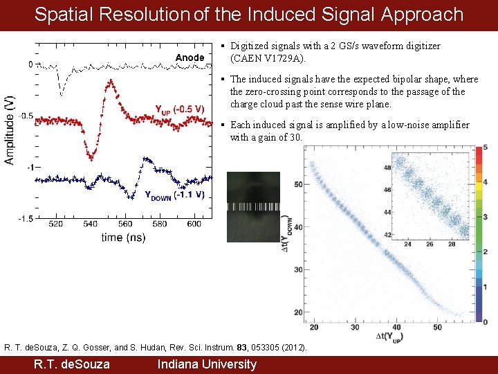
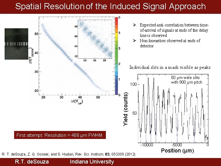
Spatial Resolution of the Induced Signal Approach § Digitized signals with a 2 GS/s waveform digitizer (CAEN V 1729 A). § The induced signals have the expected bipolar shape, where the zero-crossing point corresponds to the passage of the charge cloud past the sense wire plane. § Each induced signal is amplified by a low-noise amplifier with a gain of 30. Mask with 50 μm wide slits R. T. de. Souza, Z. Q. Gosser, and S. Hudan, Rev. Sci. Instrum. 83, 053305 (2012). R. T. de. Souza Indiana University

Spatial Resolution of the Induced Signal Approach Mask with 50 μm wide slits Ø Expected anti-correlation between timeof-arrival of signals at ends of the delay line is observed Ø Non-linearities observed at ends of detector Individual slits in a mask visible as peaks 50 μm wide slits with 900 μm pitch Yield (counts) Q 100 2 50 First attempt: Resolution = 466 μm FWHM -10000 Q 2 R. T. de. Souza, Z. Q. Gosser, and S. Hudan, Rev. Sci. Instrum. 83, 053305 (2012). R. T. de. Souza Indiana University -5000 Position (μm) 0

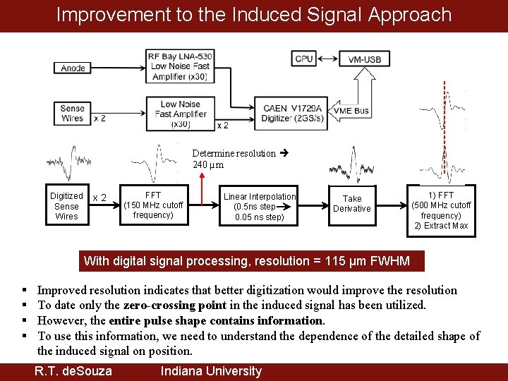
Improvement to the Induced Signal Approach Determine resolution 240 µm Digitized Sense Wires x 2 FFT (150 MHz cutoff frequency) Linear Interpolation (0. 5 ns step -> 0. 05 ns step) Take Derivative 1) FFT (500 MHz cutoff frequency) 2) Extract Max With digital signal processing, resolution = 115 μm FWHM § § Improved resolution indicates that better digitization would improve the resolution To date only the zero-crossing point in the induced signal has been utilized. However, the entire pulse shape contains information. To use this information, we need to understand the dependence of the detailed shape of the induced signal on position. R. T. de. Souza Indiana University

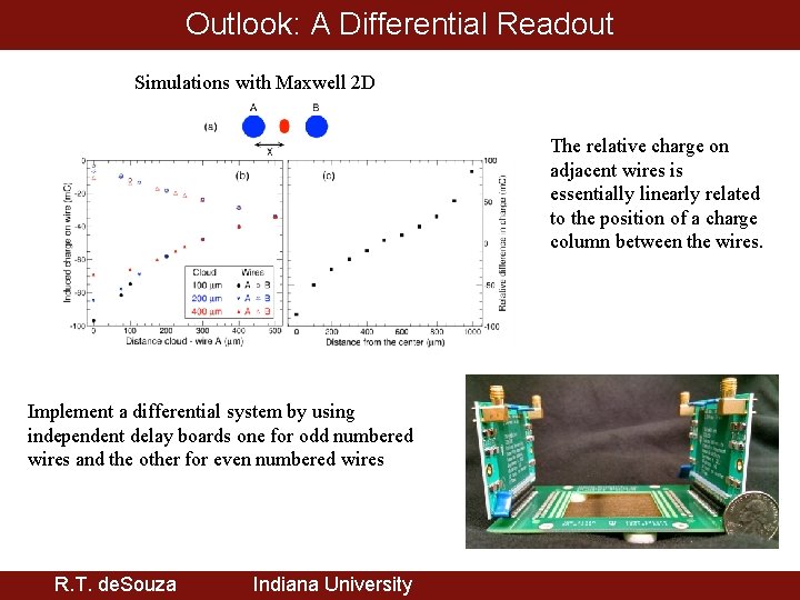
Outlook: A Differential Readout Simulations with Maxwell 2 D The relative charge on adjacent wires is essentially linearly related to the position of a charge column between the wires. Implement a differential system by using independent delay boards one for odd numbered wires and the other for even numbered wires R. T. de. Souza Indiana University

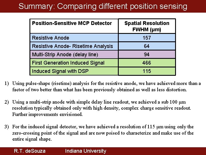
Summary: Comparing different position sensing techniques Position-Sensitive MCP Detector Spatial Resolution FWHM (μm) Resistive Anode 157 Resistive Anode- Risetime Analysis 64 Multi-Strip Anode (delay line) 94 First Generation Induced Signal 466 Induced Signal with DSP 115 1) Using pulse-shape (risetime) analysis for the resistive anode, we have achieved more than a factor of two better than what has been previously obtained as well as less distortion. 2) Using a multi-strip anode with simple delay line readout, we achieved a sub 100 μm resolution typically obtained only with high density, complex charge sensitive readout. Further improvements envisioned. 3) For the induced signal detector, we have achieved a resolution of 115 μm using only the zero-crossing point of the signal and are now poised to characterize and make use of the entire signal shape. R. T. de. Souza Indiana University

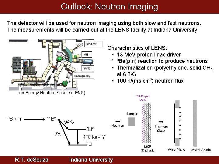
Outlook: Neutron Imaging The detector will be used for neutron imaging using both slow and fast neutrons. The measurements will be carried out at the LENS facility at Indiana University. Characteristics of LENS: § 13 Me. V proton linac driver § 9 Be(p, n) reaction to produce neutrons § Thermalization (polyethylene, solid CH 4 at 6. 5 K) § 100 n/(ms. cm 2) neutron flux Low Energy Neutron Source (LENS) 10 B +n 11 B* 6% R. T. de. Souza 94% 7 Li* 478 ke. V ϒ 7 Li Indiana University

Acknowledgements Indiana University Nuclear Chemistry: B. B. Wiggins, D. Siwal, S. Hudan, Z. de. Souza, J. Huston, T. K. Steinbach, V. Singh, J. Vadas Indiana University Chemistry Department: Mechanical Instrument Services and Electronic Instrument Services National Nuclear Security Association: Award No. DE-NA 0002012 R. T. de. Souza Indiana University

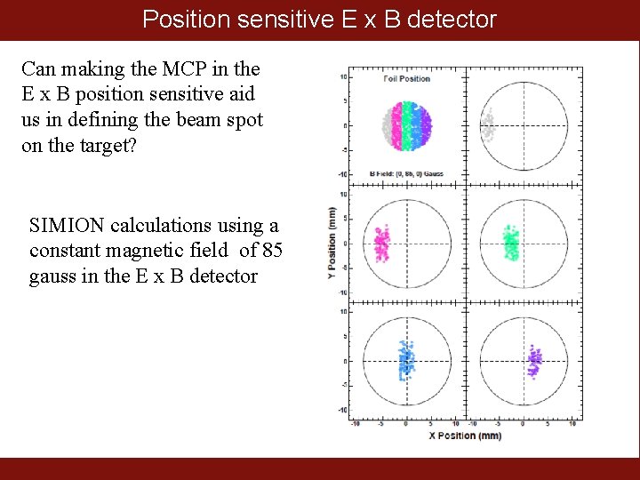
Position sensitive E x B detector Can making the MCP in the E x B position sensitive aid us in defining the beam spot on the target? SIMION calculations using a constant magnetic field of 85 gauss in the E x B detector

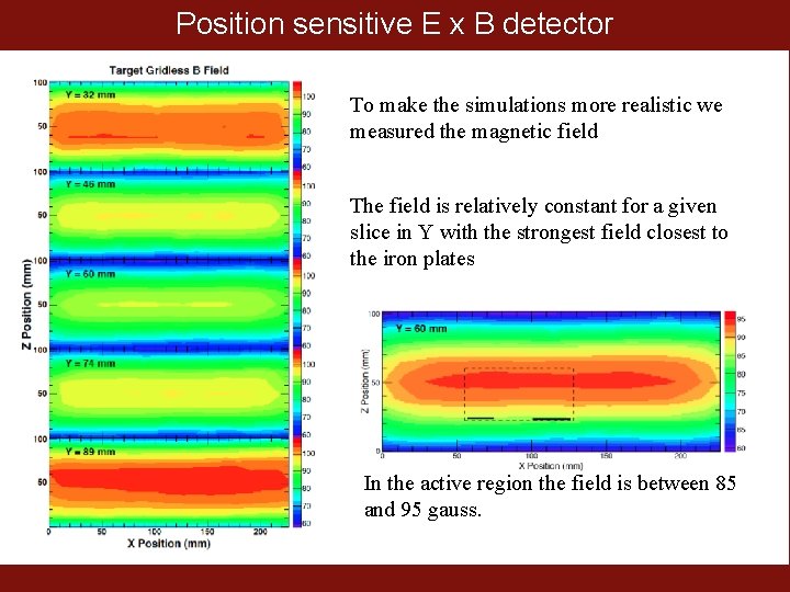
Position sensitive E x B detector To make the simulations more realistic we measured the magnetic field The field is relatively constant for a given slice in Y with the strongest field closest to the iron plates In the active region the field is between 85 and 95 gauss.

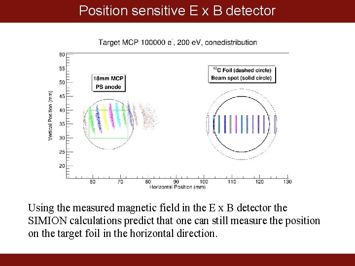
Position sensitive E x B detector Using the measured magnetic field in the E x B detector the SIMION calculations predict that one can still measure the position on the target foil in the horizontal direction.

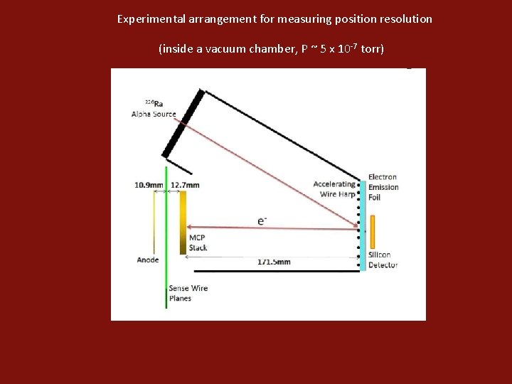
Experimental arrangement for measuring position resolution (inside a vacuum chamber, P ~ 5 x 10 -7 torr)

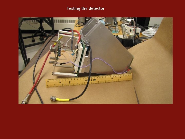
Testing the detector

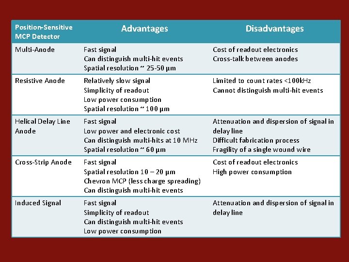
Position-Sensitive MCP Detector Advantages Disadvantages Multi-Anode Fast signal Can distinguish multi-hit events Spatial resolution ~ 25 -50 µm Cost of readout electronics Cross-talk between anodes Resistive Anode Relatively slow signal Simplicity of readout Low power consumption Spatial resolution ~ 100 µm Limited to count rates <100 k. Hz Cannot distinguish multi-hit events Helical Delay Line Anode Fast signal Low power and electronic cost Can distinguish multi-hits at 10 MHz Spatial resolution ~ 60 µm Attenuation and dispersion of signal in delay line Difficult fabrication process Fragility of a single wound wire Cross-Strip Anode Fast signal Spatial resolution 10 – 20 µm Chevron MCP (less charge spreading) Can distinguish multi-hit events Cost of readout electronics High power consumption Induced Signal Fast signal Simplicity of readout Can distinguish multi-hit events Low power consumption Attenuation and dispersion of signal in delay line