Lecture 5 Waveguides and Transmission lines Resonant Cavities
- Slides: 41

Lecture 5 Waveguides and Transmission lines Ø Resonant Cavities Ø Dielectric Slab Waveguides Ø Transmission Lines • General Properties of TEM Transmission Lines • Impedance, Inductance, and Capacitance • Transmitted Power • Power Losses, Resistance, and Conductance • Parallel Plate Lines • Microstrip Lines

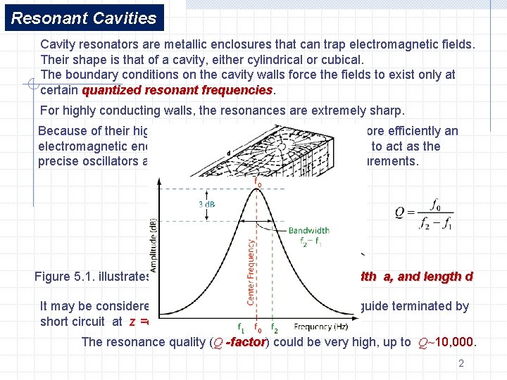
Resonant Cavities Cavity resonators are metallic enclosures that can trap electromagnetic fields. Their shape is that of a cavity, either cylindrical or cubical. The boundary conditions on the cavity walls force the fields to exist only at certain quantized resonant frequencies For highly conducting walls, the resonances are extremely sharp. Because of their high Q, cavities can be used not only to store efficiently an electromagnetic energy at microwave frequencies, but also to act as the precise oscillators and to perform precise frequency measurements. Figure 5. 1. illustrates a rectangular cavity of height b, width a, and length d It may be considered to be a section of rectangular waveguide terminated by short circuit at z =d The resonance quality (Q -factor) -factor could be very high, up to Q~10, 000. Q~ 2

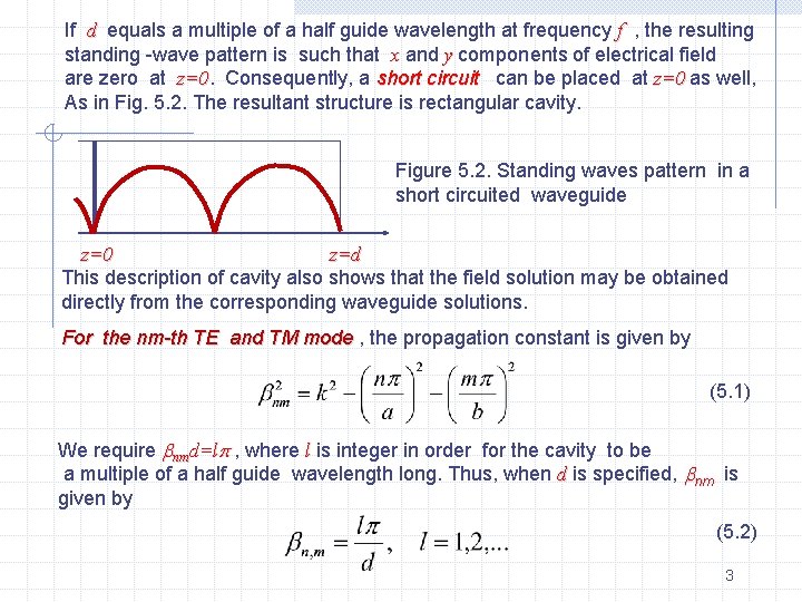
If d equals a multiple of a half guide wavelength at frequency f , the resulting standing -wave pattern is such that x and y components of electrical field are zero at z=0 Consequently, a short circuit can be placed at z=0 as well, As in Fig. 5. 2. The resultant structure is rectangular cavity. Figure 5. 2. Standing waves pattern in a short circuited waveguide z=0 z=d This description of cavity also shows that the field solution may be obtained directly from the corresponding waveguide solutions. For the nm-th TE and TM mode , the propagation constant is given by (5. 1) We require nmd=l , where l is integer in order for the cavity to be a multiple of a half guide wavelength long. Thus, when d is specified, nm is given by (5. 2) 3

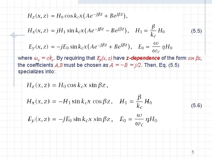
However, this relation is consistent with the earlier one only for certain discrete values k. Only if k=knml , where knml is given by (5. 3) These particular values of k give the resonant frequencies of cavity : (5. 4) where c is velocity of light. Note that • there is a triply infinite number of resonant frequencies corresponding to different field distributions, • there is more then one field solution for given resonant frequency, (5. 4) holds both TE and TM modes. since Such modes are designated as TEnml or TMnml. For simplicity, we consider the case TE 101. Eqs. (4. 67) also describe backward-moving waves if one replaces β by −β, which also changes the sign of ZH= Zω/βc Starting with a linear combination of forward and backward waves in the TE 10 mode, we obtain the field components: 4

(5. 5) where ωc = ckc. By requiring that Ey(x, z) have z-dependence of the form sin βz, βz the coefficients A, B must be chosen as A = −B = j/2. Then, Eq. (5. 5) specializes into: (5. 6) 5

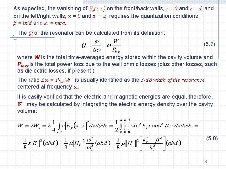
As expected, the vanishing of Ey(x, z) on the front/back walls, z = 0 and z = d, and on the left/right walls, x = 0 and x = a, requires the quantization conditions: β = lπ/d and kc = nπ/a. The Q of the resonator can be calculated from its definition: (5. 7) where W is the total time-averaged energy stored within the cavity volume and Ploss is the total power loss due to the wall ohmic losses (plus other losses, such as dielectric losses, if present. ) The ratio Δω = Ploss/W is usually identified as the 3 -d. B width of the resonance centered at frequency ω. It is easily verified that the electric and magnetic energies are equal, therefore, W may be calculated by integrating the electric energy density over the cavity volume: (5. 8) 6

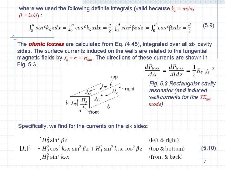
where we used the following definite integrals (valid because kc = nπ/a, β = lπ/d) lπ/d : (5. 9) The ohmic losses are calculated from Eq. (4. 45), integrated over all six cavity sides. The surface currents induced on the walls are related to the tangential magnetic fields by Js = n × Htan. The directions of these currents are shown in Fig. 5. 3. d Fig. 5. 3 Rectangular cavity resonator (and induced wall currents for the TEn 0 l mode) mode Specifically, we find for the currents on the six sides: (5. 10) 7

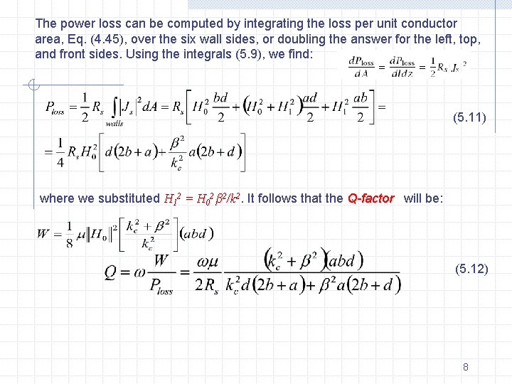
The power loss can be computed by integrating the loss per unit conductor area, Eq. (4. 45), over the six wall sides, or doubling the answer for the left, top, and front sides. Using the integrals (5. 9), we find: (5. 11) where we substituted H 12 = H 02 β 2/k 2. It follows that the Q-factor will be: (5. 12) 8

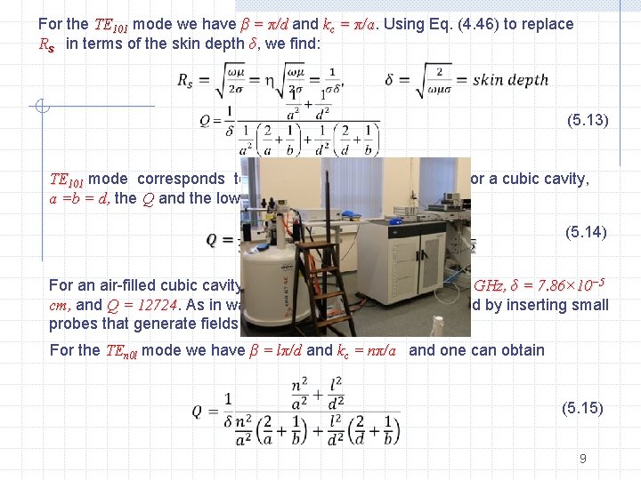
For the TE 101 mode we have β = π/d and kc = π/a Using Eq. (4. 46) to replace Rs in terms of the skin depth δ, we find: (5. 13) TE 101 mode corresponds to the lowest resonant frequency For a cubic cavity, a =b = d, the Q and the lowest resonant frequency are: (5. 14) For an air-filled cubic cavity with a = 3 cm, cm we find f 101 = 7. 07 GHz, δ = 7. 86× 10− 5 cm, and Q = 12724 As in waveguides, cavities can be excited by inserting small probes that generate fields resembling a particular mode. For the TEn 0 l mode we have β = lπ/d and kc = nπ/a and one can obtain (5. 15) 9

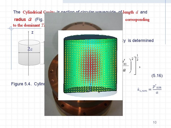
The Cylindrical Cavity is section of circular waveguide of length d and radius a (Fig. 5. 4). The lowest resonance mode is TE 111 corresponding to the dominant TE 11 mode in the circular guide. z The resonance frequency is determined from the relation 2 a d (5. 16) Figure 5. 4. Cylindrical Cavity 10

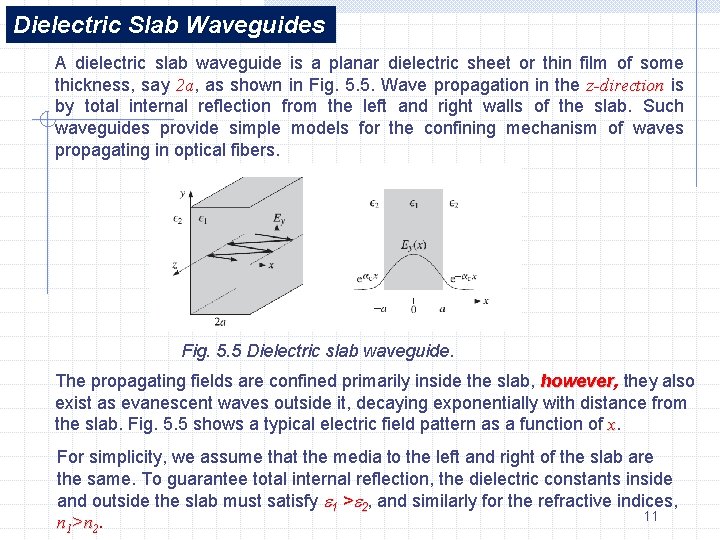
Dielectric Slab Waveguides A dielectric slab waveguide is a planar dielectric sheet or thin film of some thickness, say 2 a, 2 a as shown in Fig. 5. 5. Wave propagation in the z-direction is by total internal reflection from the left and right walls of the slab. Such waveguides provide simple models for the confining mechanism of waves propagating in optical fibers. Fig. 5. 5 Dielectric slab waveguide. The propagating fields are confined primarily inside the slab, however they also exist as evanescent waves outside it, decaying exponentially with distance from the slab. Fig. 5. 5 shows a typical electric field pattern as a function of x. For simplicity, we assume that the media to the left and right of the slab are the same. To guarantee total internal reflection, the dielectric constants inside and outside the slab must satisfy 1 > 2, and similarly for the refractive indices, 11 n 1>n 2.

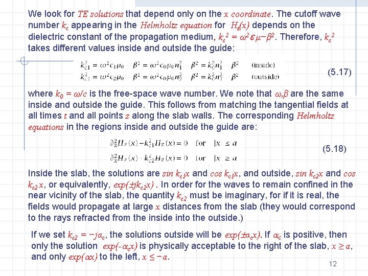
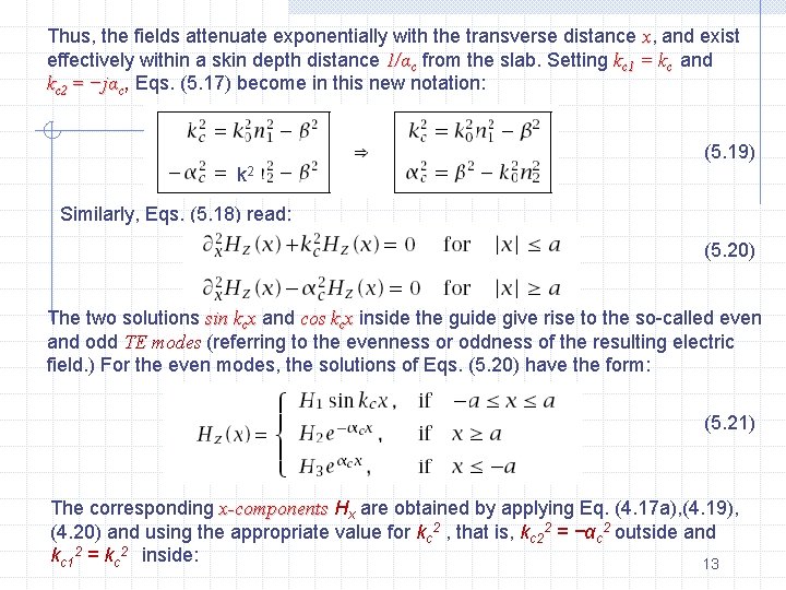
We look for TE solutions that depend only on the x coordinate The cutoff wave number kc appearing in the Helmholtz equation for Hz(x) depends on the dielectric constant of the propagation medium, kc 2 = ω2 μ−β 2. Therefore, kc 2 takes different values inside and outside the guide: (5. 17) where k 0 = ω/c is the free-space wave number. We note that ω, β are the same inside and outside the guide. This follows from matching the tangential fields at all times t and all points z along the slab walls. The corresponding Helmholtz equations in the regions inside and outside the guide are: (5. 18) Inside the slab, the solutions are sin kc 1 x and cos kc 1 x, and outside, sin kc 2 x and cos kc 2 x, or equivalently, exp( jkc 2 x). In order for the waves to remain confined in the near vicinity of the slab, the quantity kc 2 must be imaginary, for if it is real, the fields would propagate at large x distances from the slab (they would correspond to the rays refracted from the inside into the outside. ) If we set kc 2 = −jαc, the solutions outside will be exp( αcx). If c is positive, then only the solution exp(- cx) is physically acceptable to the right of the slab, x ≥ a, a and only exp( x) to the left, x ≤ −a. −a 12

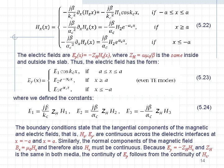
Thus, the fields attenuate exponentially with the transverse distance x, and exist effectively within a skin depth distance 1/αc from the slab. Setting kc 1 = kc and kc 2 = −jαc, Eqs. (5. 17) become in this new notation: (5. 19) k 2 Similarly, Eqs. (5. 18) read: (5. 20) The two solutions sin kcx and cos kcx inside the guide give rise to the so-called even and odd TE modes (referring to the evenness or oddness of the resulting electric field. ) For the even modes, the solutions of Eqs. (5. 20) have the form: (5. 21) The corresponding x-components Hx are obtained by applying Eq. (4. 17 a), (4. 19), (4. 20) and using the appropriate value for kc 2 , that is, kc 22 = −αc 2 outside and kc 12 = kc 2 inside: 13

(5. 22) The electric fields are Ey(x)= −ZHHx(x), where ZH = ωμ 0/β is the same inside and outside the slab. Thus, the electric field has the form: (5. 23) where we defined the constants: ZH ZH ZH (5. 24) The boundary conditions state that the tangential components of the magnetic and electric fields, that is, Hz, Ey, are continuous across the dielectric interfaces at x = −a and x = a. a Similarly, the normal components of the magnetic field Bx = μ 0 Hx and therefore also Hx must be continuous. Because Ey = −ZHHx and ZH is the same in both media, the continuity of Ey follows from the continuity of Hx. 14

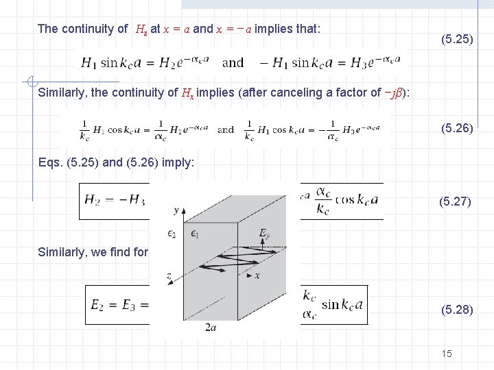
The continuity of Hz at x = a and x = −a implies that: (5. 25) Similarly, the continuity of Hx implies (after canceling a factor of −jβ): −jβ (5. 26) Eqs. (5. 25) and (5. 26) imply: (5. 27) Similarly, we find for the electric field constants: (5. 28) 15

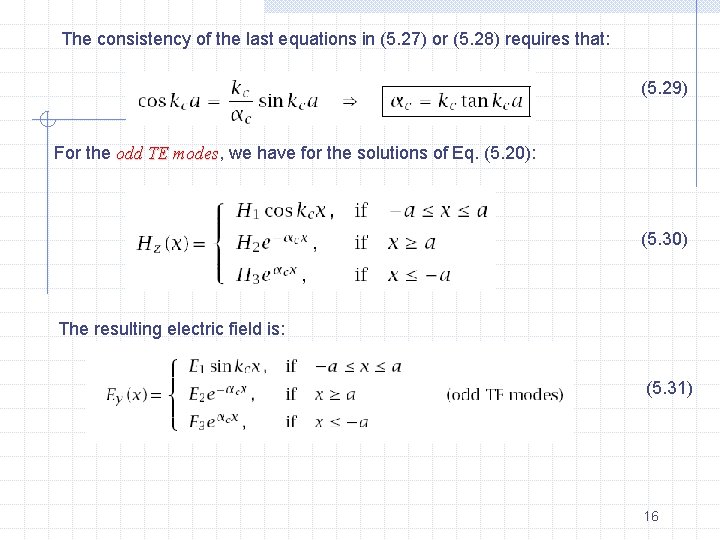
The consistency of the last equations in (5. 27) or (5. 28) requires that: (5. 29) For the odd TE modes, modes we have for the solutions of Eq. (5. 20): (5. 30) The resulting electric field is: (5. 31) 16

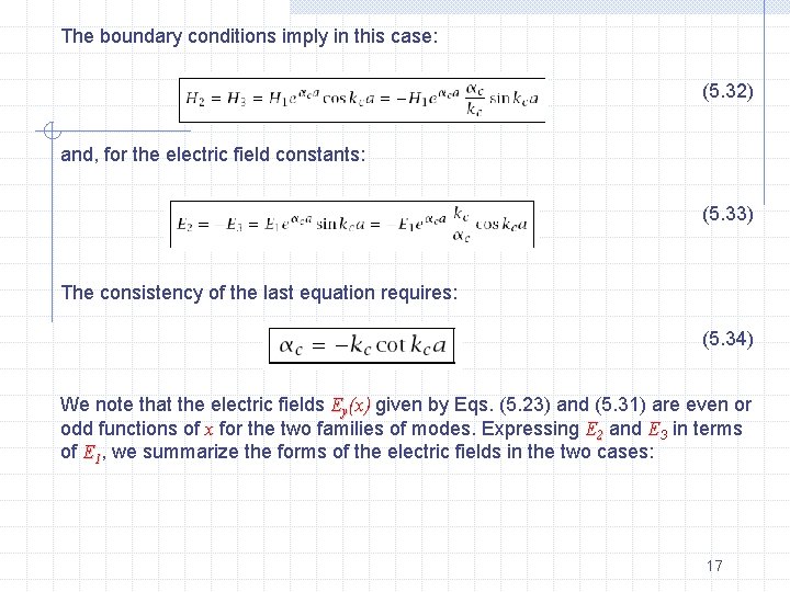
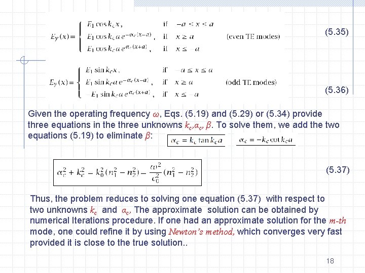
The boundary conditions imply in this case: (5. 32) and, for the electric field constants: (5. 33) The consistency of the last equation requires: (5. 34) We note that the electric fields Ey(x) given by Eqs. (5. 23) and (5. 31) are even or odd functions of x for the two families of modes. Expressing E 2 and E 3 in terms of E 1, we summarize the forms of the electric fields in the two cases: 17

(5. 35) (5. 36) Given the operating frequency ω, Eqs. (5. 19) and (5. 29) or (5. 34) provide three equations in the three unknowns kc, αc, β. β To solve them, we add the two equations (5. 19) to eliminate β: (5. 37) Thus, the problem reduces to solving one equation (5. 37) with respect to two unknowns kc and αc, The approximate solution can be obtained by numerical Iterations procedure. If one had an approximate solution for the m-th mode, one could refine it by using Newton’s method, which converges very fast provided it is close to the true solution. . 18

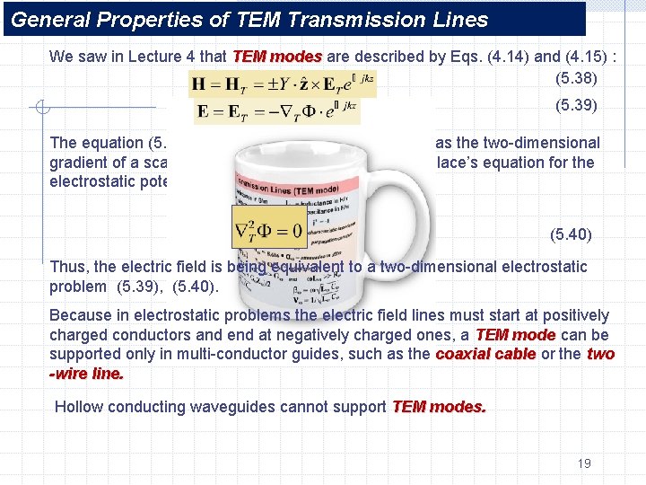
General Properties of TEM Transmission Lines We saw in Lecture 4 that TEM modes are described by Eqs. (4. 14) and (4. 15) : (5. 38) (5. 39) The equation (5. 39) implies that ET can be expressed as the two-dimensional gradient of a scalar potential which satisfy to Laplace’s equation for the electrostatic potential. (5. 40) Thus, the electric field is being equivalent to a two-dimensional electrostatic problem (5. 39), (5. 40). Because in electrostatic problems the electric field lines must start at positively charged conductors and end at negatively charged ones, a TEM mode can be supported only in multi-conductor guides, such as the coaxial cable or the two -wire line. Hollow conducting waveguides cannot support TEM modes. 19

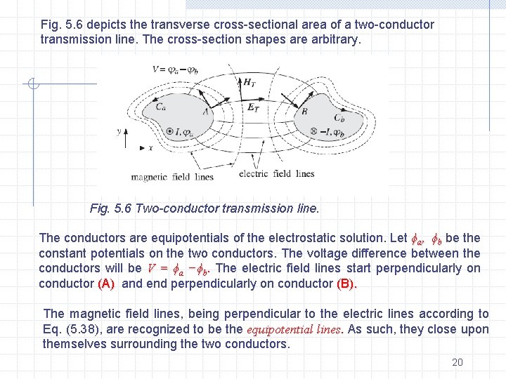
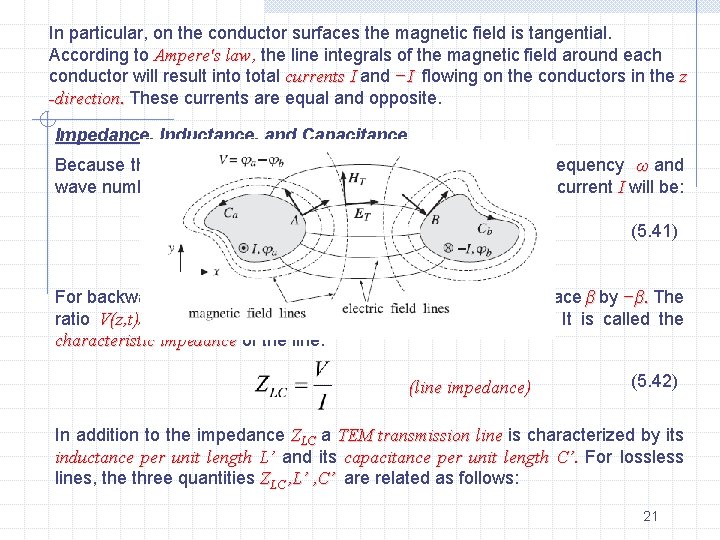
Fig. 5. 6 depicts the transverse cross-sectional area of a two-conductor transmission line. The cross-section shapes are arbitrary. Fig. 5. 6 Two-conductor transmission line. The conductors are equipotentials of the electrostatic solution. Let ϕa, ϕb be the constant potentials on the two conductors. The voltage difference between the conductors will be V = ϕa −ϕb. The electric field lines start perpendicularly on conductor (A) and end perpendicularly on conductor (B). The magnetic field lines, being perpendicular to the electric lines according to Eq. (5. 38), are recognized to be the equipotential lines. As such, they close upon themselves surrounding the two conductors. 20

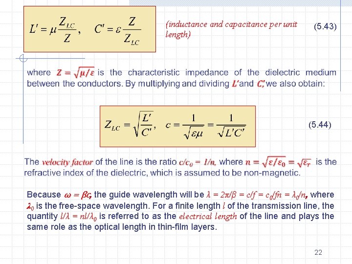
In particular, on the conductor surfaces the magnetic field is tangential. According to Ampere's law, the line integrals of the magnetic field around each conductor will result into total currents I and −I flowing on the conductors in the z -direction. These currents are equal and opposite. Impedance, Inductance, and Capacitance Because the fields are propagating along the z-direction with frequency ω and wave number β = ω/c, ω/c the z, t dependence of the voltage V and current I will be: (5. 41) For backward-moving voltage and current waves, we must replace β by −β. The ratio V(z, t)/I(z, t)=V/I remains constant and independent of z. It is called the characteristic impedance of the line: (line impedance) (5. 42) In addition to the impedance ZLC a TEM transmission line is characterized by its inductance per unit length L’ and its capacitance per unit length C’. For lossless lines, the three quantities ZLC , L’ , C’ are related as follows: 21

(inductance and capacitance per unit length) (5. 43) (5. 44) Because ω = βc, the guide wavelength will be λ = 2π/β = c/f = c 0/fn = λ 0/n, where λ 0 is the free-space wavelength. For a finite length l of the transmission line, the quantity l/λ = nl/λ 0 is referred to as the electrical length of the line and plays the same role as the optical length in thin-film layers. 22

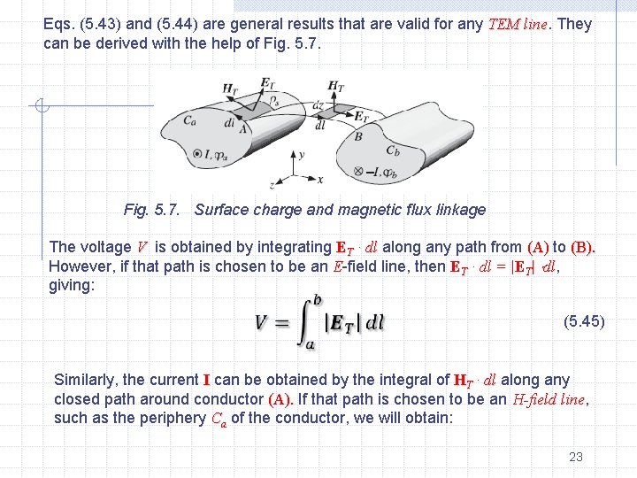
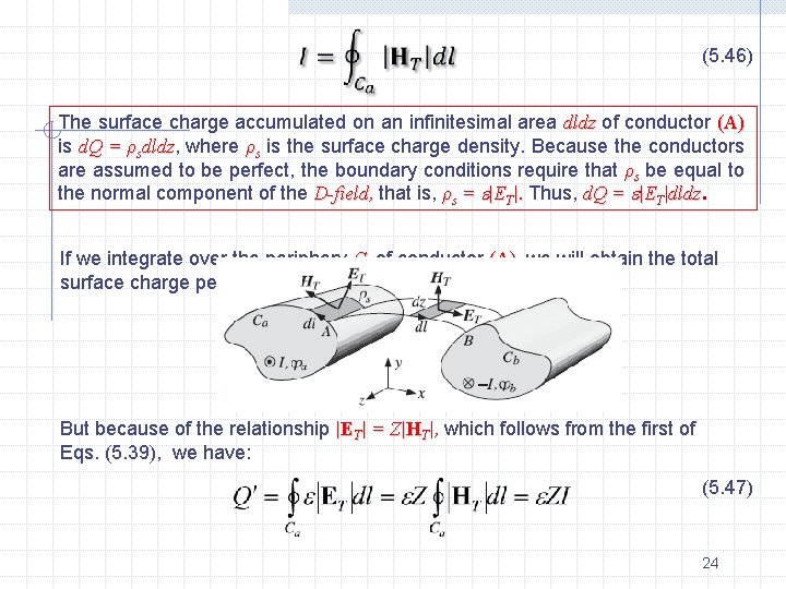
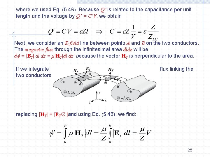
Eqs. (5. 43) and (5. 44) are general results that are valid for any TEM line They can be derived with the help of Fig. 5. 7. Surface charge and magnetic flux linkage The voltage V is obtained by integrating ET · dl along any path from (A) to (B). However, if that path is chosen to be an E-field line, then ET · dl = |ET| dl, dl giving: (5. 45) Similarly, the current I can be obtained by the integral of HT · dl along any closed path around conductor (A). If that path is chosen to be an H-field line, line such as the periphery Ca of the conductor, we will obtain: 23

(5. 46) The surface charge accumulated on an infinitesimal area dldz of conductor (A) is d. Q = ρsdldz, dldz where ρs is the surface charge density. Because the conductors are assumed to be perfect, the boundary conditions require that ρs be equal to the normal component of the D-field, that is, ρs = |ET|. Thus, d. Q = |ET|dldz If we integrate over the periphery Ca of conductor (A), we will obtain the total surface charge per unit z-length: z-length But because of the relationship |ET| = Z|HT|, which follows from the first of Eqs. (5. 39), we have: (5. 47) 24

where we used Eq. (5. 46). Because Q’ is related to the capacitance per unit length and the voltage by Q’ = C’V, C’V we obtain Next, we consider an E-field line between points A and B on the two conductors. The magnetic flux through the infinitesimal area dldz will be d = |BT| dl dz = μ|HT|dl dz because the vector HT is perpendicular to the area. If we integrate from (a) to (b), we will obtain the total magnetic flux linking the two conductors per unit z-length: replacing |HT| = |ET/Z |and using Eq. (5. 45), we find: | 25

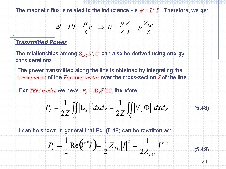
The magnetic flux is related to the inductance via ’= L’ I. Therefore, we get: Transmitted Power The relationships among ZLC, L’, C’ can also be derived using energy considerations. The power transmitted along the line is obtained by integrating the z-component of the Poynting vector over the cross-section S of the line. For TEM modes we have Pz = |ET|2/2 Z, therefore, (5. 48) It can be shown in general that Eq. (5. 48) can be rewritten as: (5. 49) 26

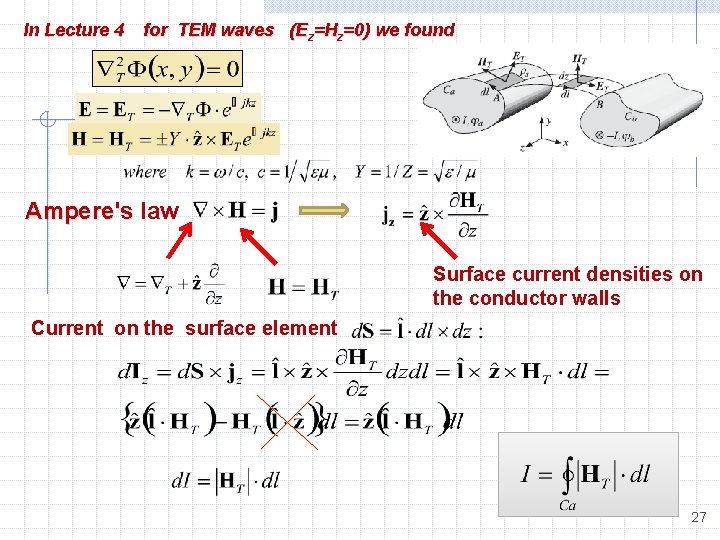
In Lecture 4 for TEM waves (Ez=Hz=0) we found Ampere's law Surface current densities on the conductor walls Current on the surface element 27

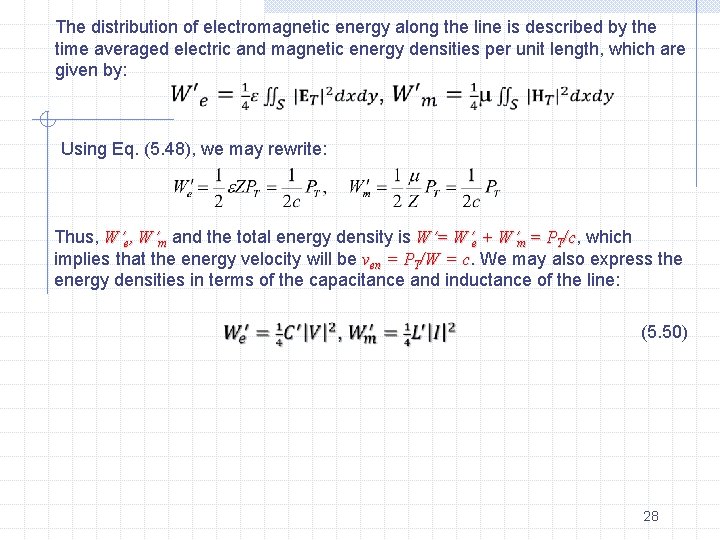
The distribution of electromagnetic energy along the line is described by the time averaged electric and magnetic energy densities per unit length, which are given by: Using Eq. (5. 48), we may rewrite: Thus, W e, W m and the total energy density is W = W e + W m = PT/c, /c which implies that the energy velocity will be ven = PT/W = c. We may also express the energy densities in terms of the capacitance and inductance of the line: (5. 50) 28

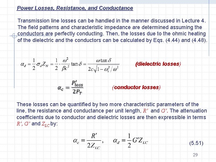
Power Losses, Resistance, and Conductance Transmission line losses can be handled in the manner discussed in Lecture 4. The field patterns and characteristic impedance are determined assuming the conductors are perfectly conducting. Then, the losses due to the ohmic heating of the dielectric and the conductors can be calculated by Eqs. (4. 44) and (4. 48). (dielectric losses) (conductor losses) These losses can be quantified by two more characteristic parameters of the line, the resistance and conductance per unit length, R’ and G’. The attenuation coefficients due to conductor and dielectric losses are then expressible in terms R’, G’ and ZLC by: (5. 51) 29

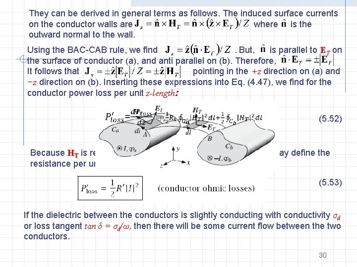
They can be derived in general terms as follows. The induced surface currents on the conductor walls are where is the outward normal to the wall. Using the BAC-CAB rule, we find. But, is parallel to ET on the surface of conductor (a), and anti parallel on (b). Therefore, It follows that pointing in the +z direction on (a) and −z direction on (b). Inserting these expressions into Eq. (4. 47), we find for the conductor power loss per unit z-length: (5. 52) Because HT is related to the total current I via Eq. (5. 46), we may define the resistance per unit length R’ through the relationship: (5. 53) If the dielectric between the conductors is slightly conducting with conductivity σd or loss tangent tan δ = σd/ω, then there will be some current flow between the two conductors. 30

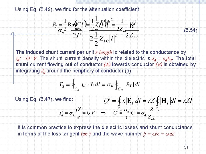
Using Eq. (5. 49), we find for the attenuation coefficient: (5. 54) The induced shunt current per unit z-length is related to the conductance by Id’ =G’ V. The shunt current density within the dielectric is Jd = σd. ET. The total shunt current flowing out of conductor (A) towards conductor (B) is obtained by integrating Jd around the periphery of conductor (a): Using Eq. (5. 47), we find: It is common practice to express the dielectric losses and shunt conductance in terms of the loss tangent tan δ and the wave number β = ω/c = ω Z: 31

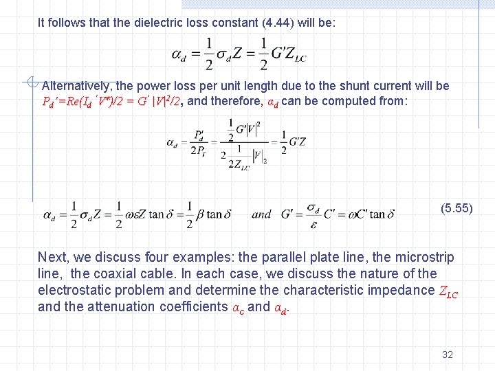
It follows that the dielectric loss constant (4. 44) will be: Alternatively, the power loss per unit length due to the shunt current will be Pd’=Re(Id ‘V∗)/2 = G’ |V|2/2, /2 and therefore, αd can be computed from: (5. 55) Next, we discuss four examples: the parallel plate line, the microstrip line, the coaxial cable. In each case, we discuss the nature of the electrostatic problem and determine the characteristic impedance ZLC and the attenuation coefficients αc and αd. 32

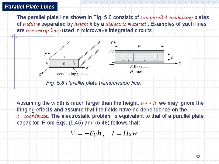
Parallel Plate Lines The parallel plate line shown in Fig. 5. 8 consists of two parallel conducting plates of width w separated by height h by a dielectric material. Examples of such lines are microstrip lines used in microwave integrated circuits. Fig. 5. 8 Parallel plate transmission line. Assuming the width is much larger than the height, w>> h, h we may ignore the fringing effects and assume that the fields have no dependence on the x - coordinate. The electrostatic problem is equivalent to that of a parallel plate capacitor. From Eqs. (5. 45) and (5. 46) follows that: 33

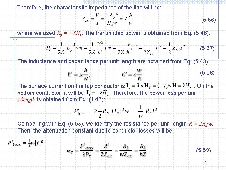
Therefore, the characteristic impedance of the line will be: (5. 56) where we used Ey = −ZHx. The transmitted power is obtained from Eq. (5. 48): (5. 57) The inductance and capacitance per unit length are obtained from Eq. (5. 43): (5. 58) The surface current on the top conductor is. On the bottom conductor, it will be. Therefore, the power loss per unit z-length is obtained from Eq. (4. 47): Comparing with Eq. (5. 53), we identify the resistance per unit length R’= 2 Rs/w. Then, the attenuation constant due to conductor losses will be: (5. 59) 34

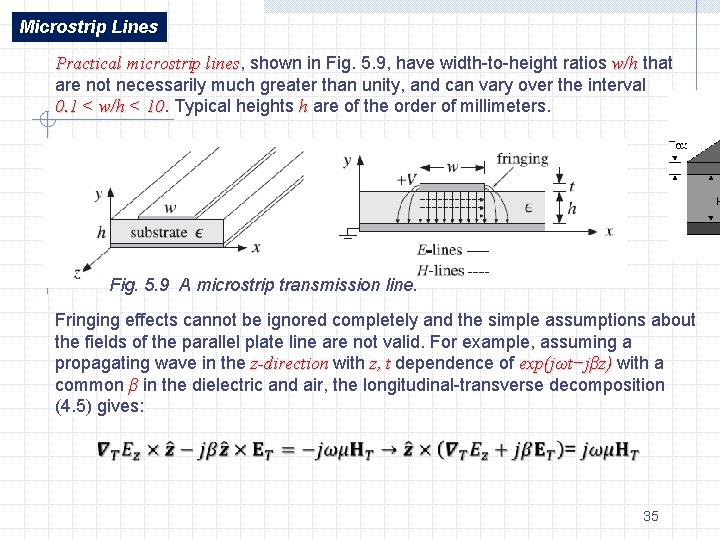
Microstrip Lines Practical microstrip lines, lines shown in Fig. 5. 9, have width-to-height ratios w/h that are not necessarily much greater than unity, and can vary over the interval 0. 1 < w/h < 10. 10 Typical heights h are of the order of millimeters. Fig. 5. 9 A microstrip transmission line. Fringing effects cannot be ignored completely and the simple assumptions about the fields of the parallel plate line are not valid. For example, assuming a propagating wave in the z-direction with z, t dependence of exp(jωt−jβz) with a common β in the dielectric and air, the longitudinal-transverse decomposition (4. 5) gives: 35

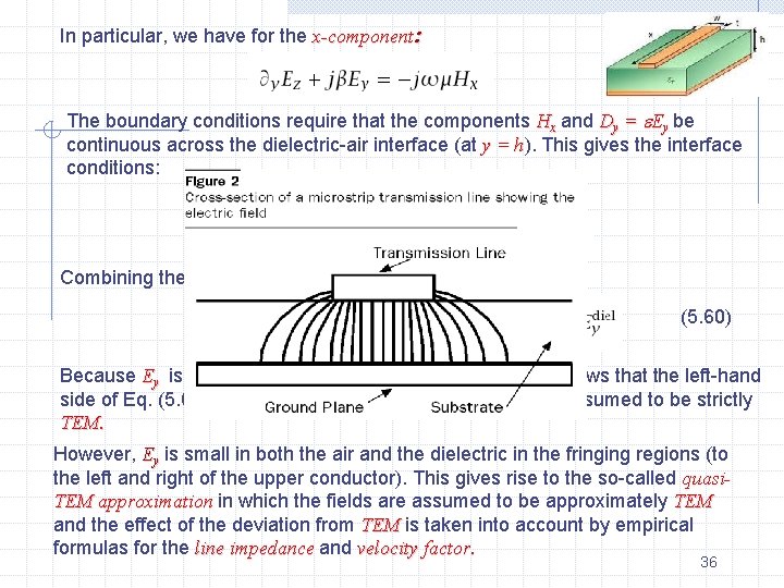
In particular, we have for the x-component: The boundary conditions require that the components Hx and Dy = Ey be continuous across the dielectric-air interface (at y = h). h This gives the interface conditions: Combining the two conditions, we obtain: (5. 60) Because Ey is non-zero on either side of the interface, it follows that the left-hand side of Eq. (5. 60) cannot be zero and the wave cannot be assumed to be strictly TEM. However, Ey is small in both the air and the dielectric in the fringing regions (to the left and right of the upper conductor). This gives rise to the so-called quasi. TEM approximation in which the fields are assumed to be approximately TEM and the effect of the deviation from TEM is taken into account by empirical formulas for the line impedance and velocity factor. 36

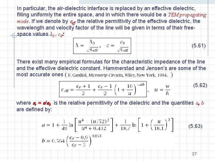
In particular, the air-dielectric interface is replaced by an effective dielectric, filling uniformly the entire space, and in which there would be a TEM propagating mode If we denote by eff the relative permittivity of the effective dielectric, the wavelength and velocity factor of the line will be given in terms of their freespace values λ 0 , c 0: (5. 61) There exist many empirical formulas for the characteristic impedance of the line and the effective dielectric constant. Hammerstad and Jensen’s are some of the most accurate ones ( ) ) (5. 62) where r = / 0 is the relative permittivity of the dielectric and the quantities a, b are defined by: (5. 63) 37

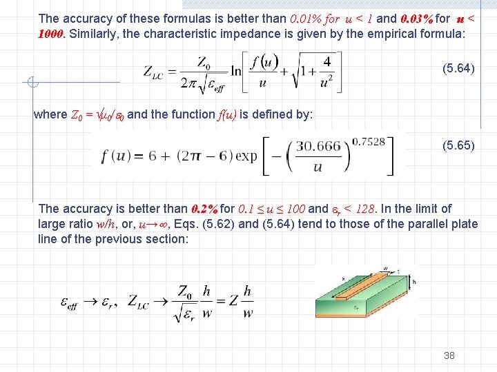
The accuracy of these formulas is better than 0. 01% for u < 1 and 0. 03% for u < 1000. Similarly, the characteristic impedance is given by the empirical formula: (5. 64) where Z 0 = μ 0/ 0 and the function f(u) is defined by: (5. 65) The accuracy is better than 0. 2% for 0. 1 ≤ u ≤ 100 and r < 128 In the limit of large ratio w/h, w/h or, u→ , Eqs. (5. 62) and (5. 64) tend to those of the parallel plate line of the previous section: 38

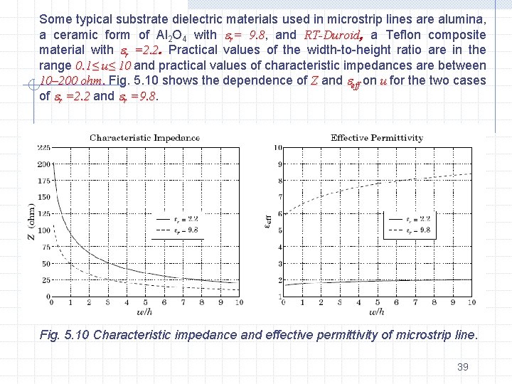
Some typical substrate dielectric materials used in microstrip lines are alumina, a ceramic form of Al 2 O 4 with r= 9. 8, 9. 8 and RT-Duroid, a Teflon composite material with r =2. 2. Practical values of the width-to-height ratio are in the range 0. 1≤ u≤ 10 and practical values of characteristic impedances are between 10– 200 ohm. Fig. 5. 10 shows the dependence of Z and eff on u for the two cases of r =2. 2 and r =9. 8 Fig. 5. 10 Characteristic impedance and effective permittivity of microstrip line. 39

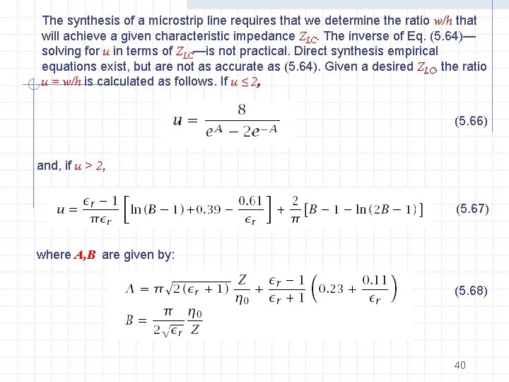
The synthesis of a microstrip line requires that we determine the ratio w/h that will achieve a given characteristic impedance ZLC. The inverse of Eq. (5. 64)— solving for u in terms of ZLC—is not practical. Direct synthesis empirical equations exist, but are not as accurate as (5. 64). Given a desired ZLC, the ratio u = w/h is calculated as follows. If u ≤ 2, (5. 66) and, if u > 2, 2 (5. 67) where A, B are given by: (5. 68) 40

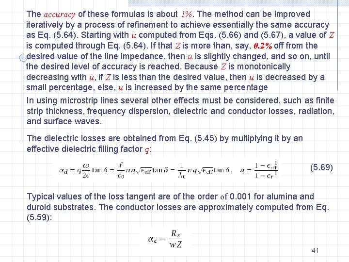
The accuracy of these formulas is about 1%. 1% The method can be improved iteratively by a process of refinement to achieve essentially the same accuracy as Eq. (5. 64). Starting with u computed from Eqs. (5. 66) and (5. 67), a value of Z is computed through Eq. (5. 64). If that Z is more than, say, 0. 2% off from the desired value of the line impedance, then u is slightly changed, and so on, until the desired level of accuracy is reached. Because Z is monotonically decreasing with u, if Z is less than the desired value, then u is decreased by a small percentage, else, u is increased by the same percentage In using microstrip lines several other effects must be considered, such as finite strip thickness, frequency dispersion, dielectric and conductor losses, radiation, and surface waves. The dielectric losses are obtained from Eq. (5. 45) by multiplying it by an effective dielectric filling factor q: (5. 69) Typical values of the loss tangent are of the order of 0. 001 for alumina and duroid substrates. The conductor losses are approximately computed from Eq. (5. 59): 41