19 4 Loaddependent properties of resonant converters Resonant
- Slides: 28

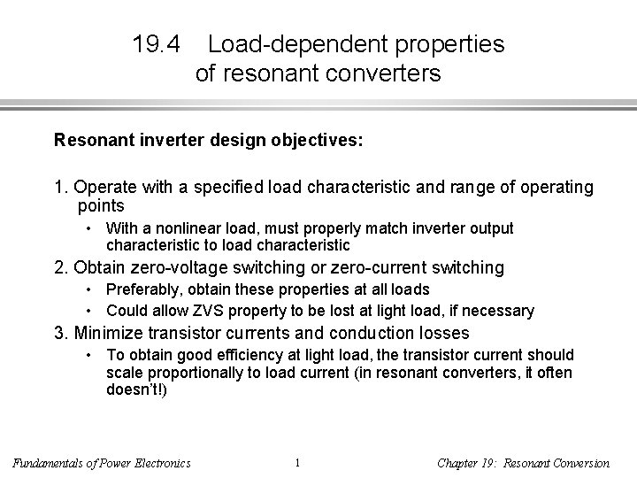
19. 4 Load-dependent properties of resonant converters Resonant inverter design objectives: 1. Operate with a specified load characteristic and range of operating points • With a nonlinear load, must properly match inverter output characteristic to load characteristic 2. Obtain zero-voltage switching or zero-current switching • Preferably, obtain these properties at all loads • Could allow ZVS property to be lost at light load, if necessary 3. Minimize transistor currents and conduction losses • To obtain good efficiency at light load, the transistor current should scale proportionally to load current (in resonant converters, it often doesn’t!) Fundamentals of Power Electronics 1 Chapter 19: Resonant Conversion

Topics of Discussion Section 19. 4 Inverter output i-v characteristics Two theorems • Dependence of transistor current on load current • Dependence of zero-voltage/zero-current switching on load resistance • Simple, intuitive frequency-domain approach to design of resonant converter Examples and interpretation • Series • Parallel • LCC Fundamentals of Power Electronics 2 Chapter 19: Resonant Conversion

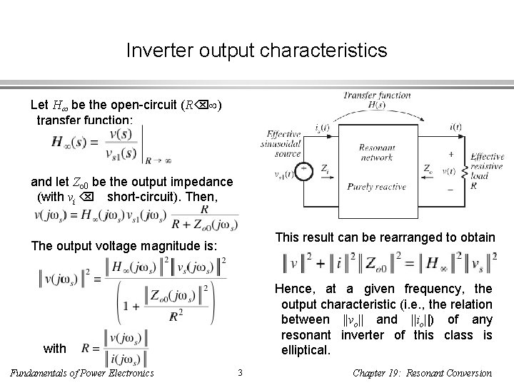
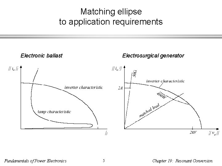
Inverter output characteristics Let H be the open-circuit (R ) transfer function: and let Zo 0 be the output impedance (with vi short-circuit). Then, This result can be rearranged to obtain The output voltage magnitude is: Hence, at a given frequency, the output characteristic (i. e. , the relation between ||vo|| and ||io||) of any resonant inverter of this class is elliptical. with Fundamentals of Power Electronics 3 Chapter 19: Resonant Conversion

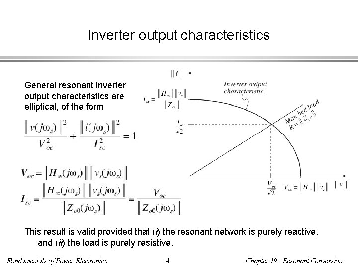
Inverter output characteristics General resonant inverter output characteristics are elliptical, of the form This result is valid provided that (i) the resonant network is purely reactive, and (ii) the load is purely resistive. Fundamentals of Power Electronics 4 Chapter 19: Resonant Conversion

Matching ellipse to application requirements Electronic ballast Fundamentals of Power Electronics Electrosurgical generator 5 Chapter 19: Resonant Conversion

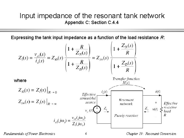
Input impedance of the resonant tank network Appendix C: Section C. 4. 4 Expressing the tank input impedance as a function of the load resistance R: where Fundamentals of Power Electronics 6 Chapter 19: Resonant Conversion

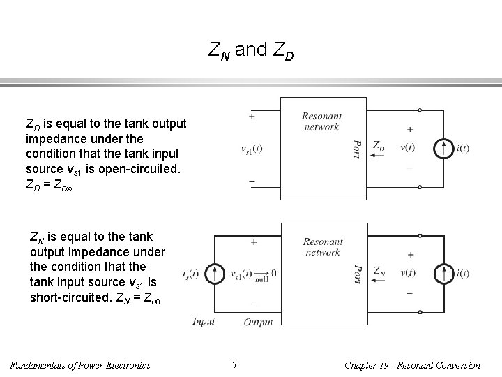
ZN and ZD ZD is equal to the tank output impedance under the condition that the tank input source vs 1 is open-circuited. ZD = Zo ZN is equal to the tank output impedance under the condition that the tank input source vs 1 is short-circuited. ZN = Zo 0 Fundamentals of Power Electronics 7 Chapter 19: Resonant Conversion

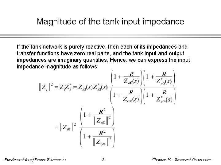
Magnitude of the tank input impedance If the tank network is purely reactive, then each of its impedances and transfer functions have zero real parts, and the tank input and output impedances are imaginary quantities. Hence, we can express the input impedance magnitude as follows: Fundamentals of Power Electronics 8 Chapter 19: Resonant Conversion

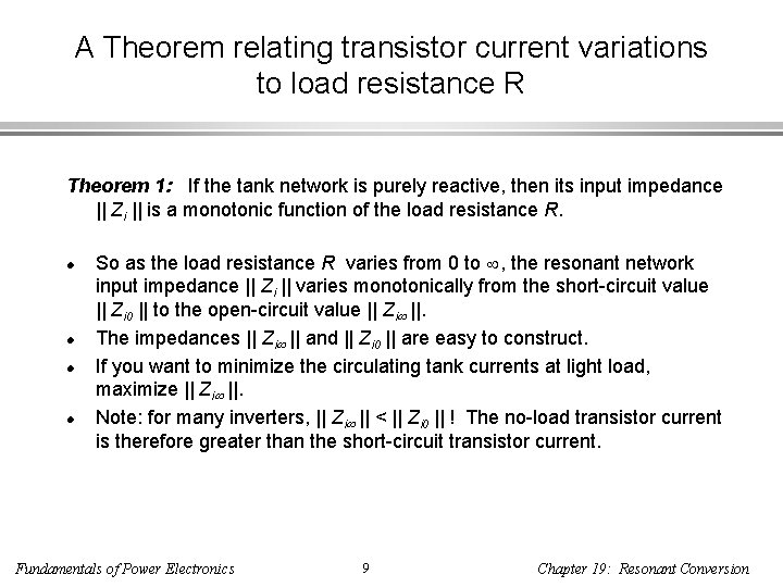
A Theorem relating transistor current variations to load resistance R Theorem 1: If the tank network is purely reactive, then its input impedance || Zi || is a monotonic function of the load resistance R. So as the load resistance R varies from 0 to , the resonant network input impedance || Zi || varies monotonically from the short-circuit value || Zi 0 || to the open-circuit value || Zi ||. The impedances || Zi || and || Zi 0 || are easy to construct. If you want to minimize the circulating tank currents at light load, maximize || Zi ||. Note: for many inverters, || Zi || < || Zi 0 || ! The no-load transistor current is therefore greater than the short-circuit transistor current. Fundamentals of Power Electronics 9 Chapter 19: Resonant Conversion

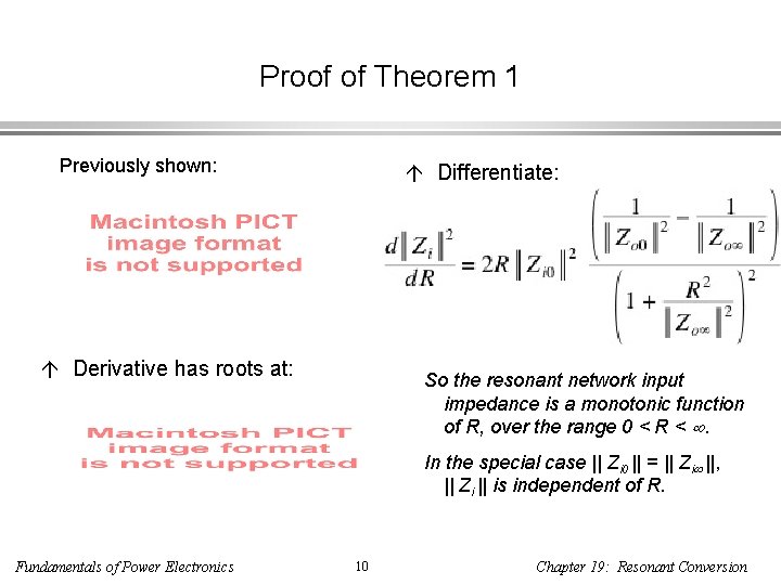
Proof of Theorem 1 Previously shown: Differentiate: Derivative has roots at: So the resonant network input impedance is a monotonic function of R, over the range 0 < R < . In the special case || Zi 0 || = || Zi ||, || Zi || is independent of R. Fundamentals of Power Electronics 10 Chapter 19: Resonant Conversion

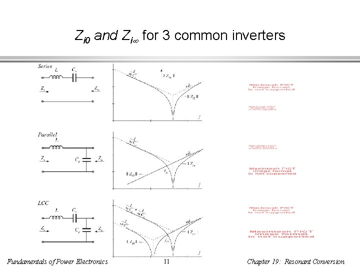
Zi 0 and Zi for 3 common inverters Fundamentals of Power Electronics 11 Chapter 19: Resonant Conversion

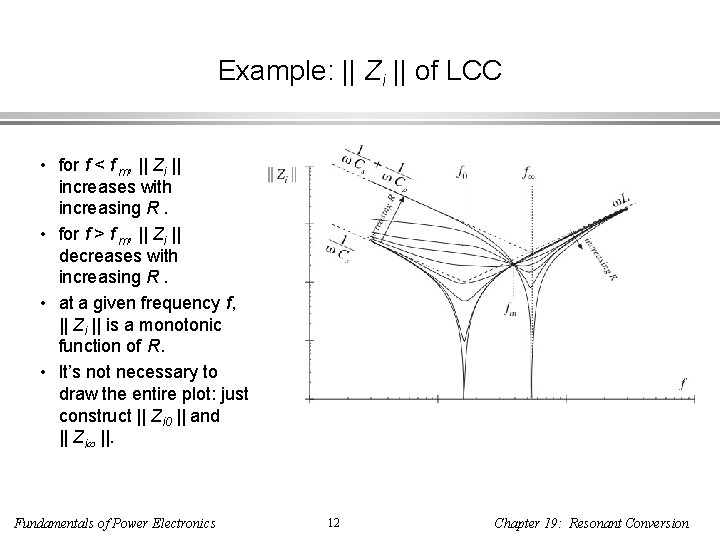
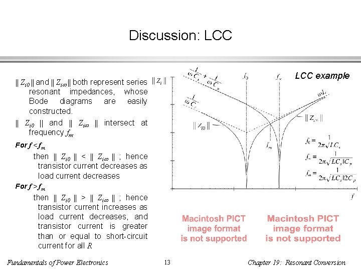
Example: || Zi || of LCC • for f < f m, || Zi || increases with increasing R. • for f > f m, || Zi || decreases with increasing R. • at a given frequency f, || Zi || is a monotonic function of R. • It’s not necessary to draw the entire plot: just construct || Zi 0 || and || Zi ||. Fundamentals of Power Electronics 12 Chapter 19: Resonant Conversion

Discussion: LCC example || Zi 0 || and || Zi || both represent series resonant impedances, whose Bode diagrams are easily constructed. || Zi 0 || and || Zi || intersect at frequency fm. For f < fm then || Zi 0 || < || Zi || ; hence transistor current decreases as load current decreases For f > fm then || Zi 0 || > || Zi || ; hence transistor current increases as load current decreases, and transistor current is greater than or equal to short-circuit current for all R Fundamentals of Power Electronics 13 Chapter 19: Resonant Conversion

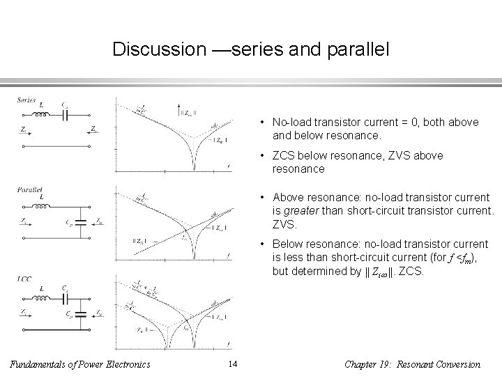
Discussion —series and parallel • No-load transistor current = 0, both above and below resonance. • ZCS below resonance, ZVS above resonance • Above resonance: no-load transistor current is greater than short-circuit transistor current. ZVS. • Below resonance: no-load transistor current is less than short-circuit current (for f <fm), but determined by || Zi ||. ZCS. Fundamentals of Power Electronics 14 Chapter 19: Resonant Conversion

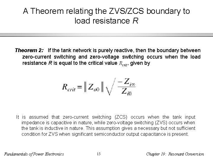
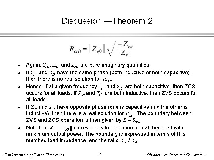
A Theorem relating the ZVS/ZCS boundary to load resistance R Theorem 2: If the tank network is purely reactive, then the boundary between zero-current switching and zero-voltage switching occurs when the load resistance R is equal to the critical value Rcrit, given by It is assumed that zero-current switching (ZCS) occurs when the tank input impedance is capacitive in nature, while zero-voltage switching (ZVS) occurs when the tank is inductive in nature. This assumption gives a necessary but not sufficient condition for ZVS when significant semiconductor output capacitance is present. Fundamentals of Power Electronics 15 Chapter 19: Resonant Conversion

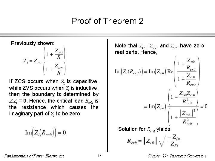
Proof of Theorem 2 Previously shown: Note that Zi , Zo 0, and Zo have zero real parts. Hence, If ZCS occurs when Zi is capacitive, while ZVS occurs when Zi is inductive, then the boundary is determined by Zi = 0. Hence, the critical load Rcrit is the resistance which causes the imaginary part of Zi to be zero: Solution for Rcrit yields Fundamentals of Power Electronics 16 Chapter 19: Resonant Conversion

Discussion —Theorem 2 Again, Zi 0, and Zo 0 are pure imaginary quantities. If Zi and Zi 0 have the same phase (both inductive or both capacitive), then there is no real solution for Rcrit. Hence, if at a given frequency Zi and Zi 0 are both capacitive, then ZCS occurs for all loads. If Zi and Zi 0 are both inductive, then ZVS occurs for all loads. If Zi and Zi 0 have opposite phase (one is capacitive and the other is inductive), then there is a real solution for Rcrit. The boundary between ZVS and ZCS operation is then given by R = Rcrit. Note that R = || Zo 0 || corresponds to operation at matched load with maximum output power. The boundary is expressed in terms of this matched load impedance, and the ratio Zi / Zi 0. Fundamentals of Power Electronics 17 Chapter 19: Resonant Conversion

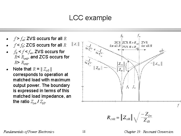
LCC example f > f : ZVS occurs for all R f < f 0: ZCS occurs for all R f 0 < f , ZVS occurs for R< Rcrit, and ZCS occurs for R> Rcrit. Note that R = || Zo 0 || corresponds to operation at matched load with maximum output power. The boundary is expressed in terms of this matched load impedance, and the ratio Zi / Zi 0. Fundamentals of Power Electronics 18 Chapter 19: Resonant Conversion

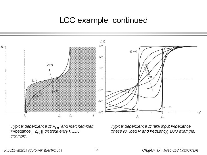
LCC example, continued Typical dependence of Rcrit and matched-load impedance || Zo 0 || on frequency f, LCC example. Fundamentals of Power Electronics Typical dependence of tank input impedance phase vs. load R and frequency, LCC example. 19 Chapter 19: Resonant Conversion

19. 4. 4 Design Example Select resonant tank elements to design a resonant inverter that meets the following requirements: • Switching frequency fs = 100 k. Hz • Input voltage Vg = 160 V • Inverter is capable of producing a peak open circuit output voltage of 400 V • Inverter can produce a nominal output of 150 Vrms at 25 W Fundamentals of Power Electronics 20 Chapter 19: Resonant Conversion

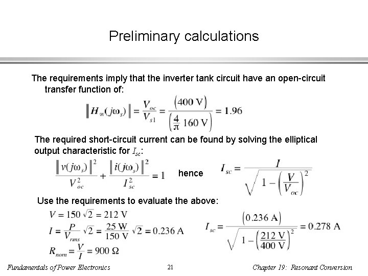
Preliminary calculations The requirements imply that the inverter tank circuit have an open-circuit transfer function of: The required short-circuit current can be found by solving the elliptical output characteristic for Isc: hence Use the requirements to evaluate the above: Fundamentals of Power Electronics 21 Chapter 19: Resonant Conversion

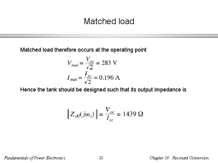
Matched load therefore occurs at the operating point Hence the tank should be designed such that its output impedance is Fundamentals of Power Electronics 22 Chapter 19: Resonant Conversion

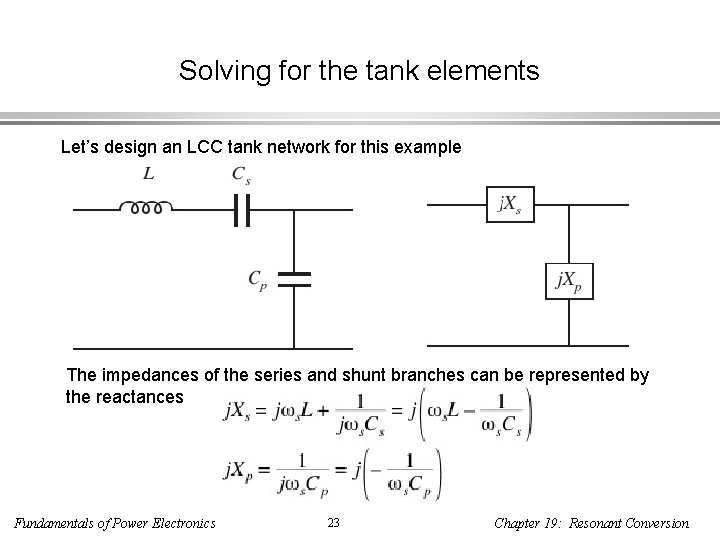
Solving for the tank elements Let’s design an LCC tank network for this example The impedances of the series and shunt branches can be represented by the reactances Fundamentals of Power Electronics 23 Chapter 19: Resonant Conversion

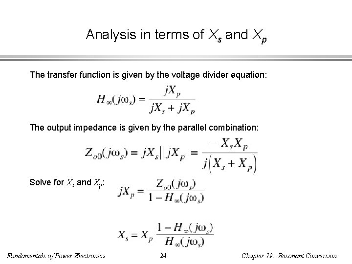
Analysis in terms of Xs and Xp The transfer function is given by the voltage divider equation: The output impedance is given by the parallel combination: Solve for Xs and Xp: Fundamentals of Power Electronics 24 Chapter 19: Resonant Conversion

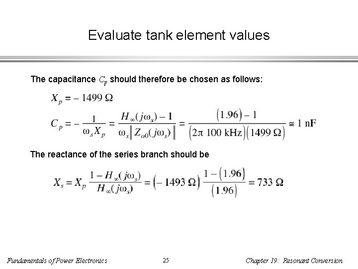
Evaluate tank element values The capacitance Cp should therefore be chosen as follows: The reactance of the series branch should be Fundamentals of Power Electronics 25 Chapter 19: Resonant Conversion

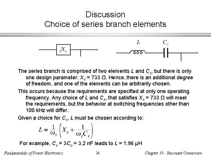
Discussion Choice of series branch elements The series branch is comprised of two elements L and Cs, but there is only one design parameter: Xs = 733 Ω. Hence, there is an additional degree of freedom, and one of the elements can be arbitrarily chosen. This occurs because the requirements are specified at only one operating frequency. Any choice of L and Cs, that satisfies Xs = 733 Ω will meet the requirements, but the behavior at switching frequencies other than 100 k. Hz will differ. Given a choice for Cs, L must be chosen according to: For example, Cs = 3 Cp = 3. 2 n. F leads to L = 1. 96 µH Fundamentals of Power Electronics 26 Chapter 19: Resonant Conversion

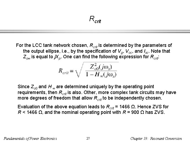
Rcrit For the LCC tank network chosen, Rcrit is determined by the parameters of the output ellipse, i. e. , by the specification of Vg, Voc, and Isc. Note that Zo is equal to j. Xp. One can find the following expression for Rcrit: Since Zo 0 and H are determined uniquely by the operating point requirements, then Rcrit is also. Other, more complex tank circuits may have more degrees of freedom that allow Rcrit to be independently chosen. Evaluation of the above equation leads to Rcrit = 1466 Ω. Hence ZVS for R < 1466 Ω, and the nominal operating point with R = 900 Ω has ZVS. Fundamentals of Power Electronics 27 Chapter 19: Resonant Conversion

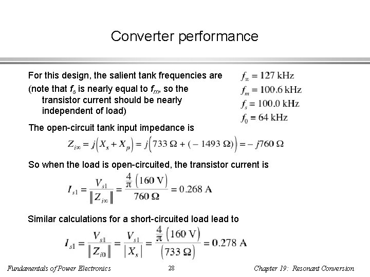
Converter performance For this design, the salient tank frequencies are (note that fs is nearly equal to fm, so the transistor current should be nearly independent of load) The open-circuit tank input impedance is So when the load is open-circuited, the transistor current is Similar calculations for a short-circuited load lead to Fundamentals of Power Electronics 28 Chapter 19: Resonant Conversion