LDO Architecture Review How different LDO architectures influence



- Slides: 36

LDO Architecture Review How different LDO architectures influence performance 1

Overview • General Block Diagram Review • Small Signal Model • LDO Pass Devices – PMOS – NMOS – BJT • LDO Performance – – Dropout Noise PSRR Startup 2

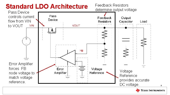
Standard LDO Architecture Pass Device controls current flow from VIN to VOUT Error Amplifier forces FB node voltage to match voltage reference. Feedback Resistors determine output voltage Voltage Reference provides accurate DC voltage. 3

Overview • General Block Diagram Review • Small Signal Model • LDO Pass Devices – PMOS – NMOS – BJT • LDO Performance – – Dropout Noise PSRR Startup 4

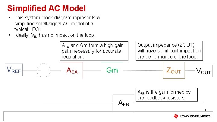
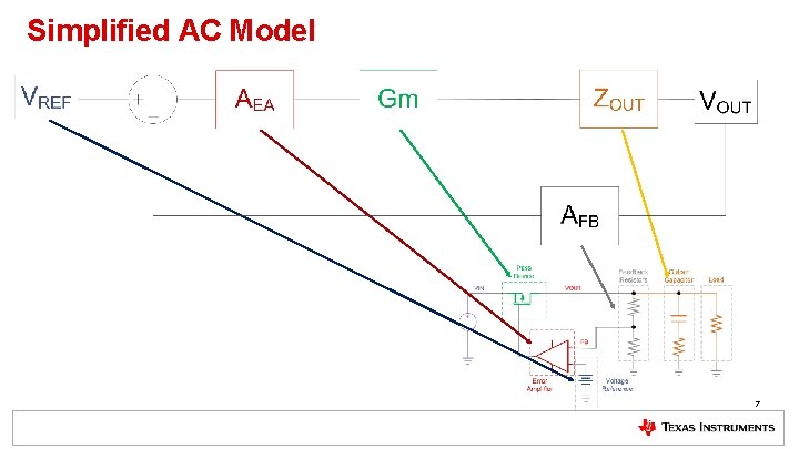
Simplified AC Model • This system block diagram represents a simplified small-signal AC model of a typical LDO. • Ideally, VIN has no impact on the loop. AEA and Gm form a high-gain path necessary for accurate regulation. Output impedance (ZOUT) will have significant impact on the performance of the loop. AFB is the gain formed by the feedback resistors. 5

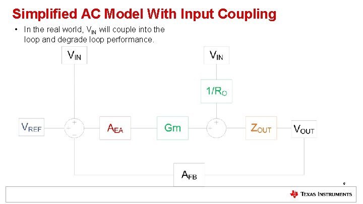
Simplified AC Model With Input Coupling • In the real world, VIN will couple into the loop and degrade loop performance. 6

Simplified AC Model 7

Overview • General Block Diagram Review • Small Signal Model • LDO Pass Devices – PMOS – NMOS – BJT • LDO Performance – – Dropout Noise PSRR Startup 8

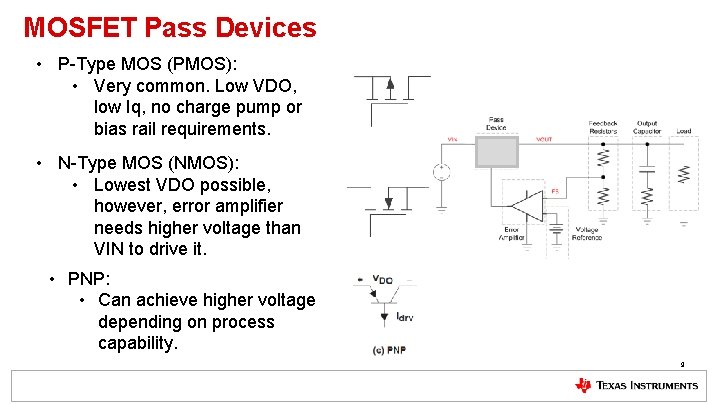
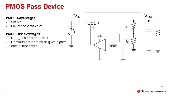
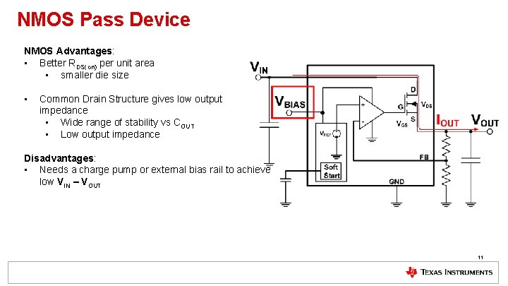
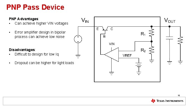
MOSFET Pass Devices • P-Type MOS (PMOS): • Very common. Low VDO, low Iq, no charge pump or bias rail requirements. • N-Type MOS (NMOS): • Lowest VDO possible, however, error amplifier needs higher voltage than VIN to drive it. • PNP: • Can achieve higher voltage depending on process capability. 9

PMOS Pass Device PMOS Advantages: • Simple • Lowest cost structure PMOS Disadvantages: • RDSON is higher vs. NMOS • Common-drain structure gives higher output impedance 10

NMOS Pass Device NMOS Advantages: • Better RDS(on) per unit area • smaller die size • Common Drain Structure gives low output impedance • Wide range of stability vs COUT • Low output impedance Disadvantages: • Needs a charge pump or external bias rail to achieve low VIN – VOUT 11

PNP Pass Device PNP Advantages: • Can achieve higher VIN voltages • Error amplifier design in bipolar process can achieve low noise Disadvantages: • Difficult to design for low Iq • Dropout can be higher for light loads 12

Overview • General Block Diagram Review • Small Signal Model • LDO Pass Devices – PMOS – NMOS – BJT • LDO Performance – – Dropout Noise PSRR Startup 13

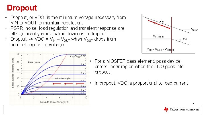
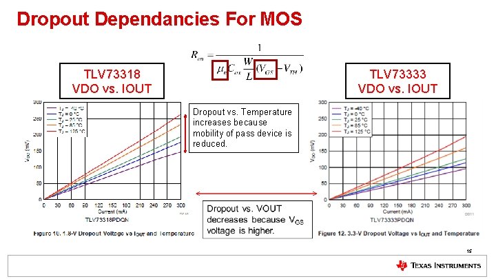
Dropout • Dropout, or VDO, is the minimum voltage necessary from VIN to VOUT to maintain regulation. • PSRR, noise, load regulation and transient response are all significantly worse when device is in dropout. • Dropout -> VDO = VIN – VOUT when VOUT drops from nominal regulation voltage • For a MOSFET pass element, pass device enters linear region when the LDO goes into dropout. • In dropout, VDO is proportional to load current 14

Dropout Dependancies For MOS TLV 73318 VDO vs. IOUT TLV 73333 VDO vs. IOUT Dropout vs. Temperature increases because mobility of pass device is reduced. 15

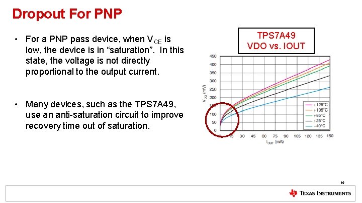
Dropout For PNP • For a PNP pass device, when VCE is low, the device is in “saturation”. In this state, the voltage is not directly proportional to the output current. TPS 7 A 49 VDO vs. IOUT • Many devices, such as the TPS 7 A 49, use an anti-saturation circuit to improve recovery time out of saturation. 16

Overview • General Block Diagram Review • Small Signal Model • LDO Pass Devices – PMOS – NMOS – BJT • LDO Performance – – Dropout Noise PSRR Startup 17

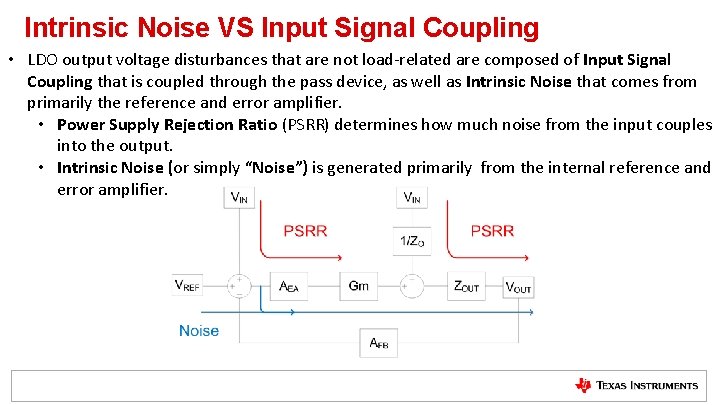
Intrinsic Noise VS Input Signal Coupling • LDO output voltage disturbances that are not load-related are composed of Input Signal Coupling that is coupled through the pass device, as well as Intrinsic Noise that comes from primarily the reference and error amplifier. • Power Supply Rejection Ratio (PSRR) determines how much noise from the input couples into the output. • Intrinsic Noise (or simply “Noise”) is generated primarily from the internal reference and error amplifier.

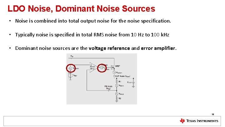
LDO Noise, Dominant Noise Sources • Noise is combined into total output noise for the noise specification. • Typically noise is specified in total RMS noise from 10 Hz to 100 k. Hz • Dominant noise sources are the voltage reference and error amplifier. 19

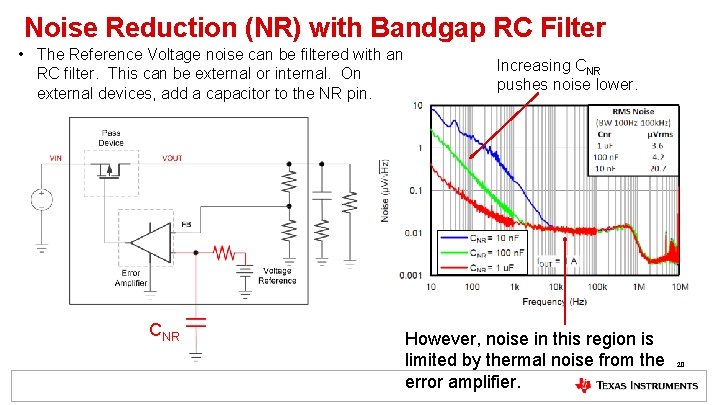
Noise Reduction (NR) with Bandgap RC Filter • The Reference Voltage noise can be filtered with an RC filter. This can be external or internal. On external devices, add a capacitor to the NR pin. CNR Increasing CNR pushes noise lower. However, noise in this region is limited by thermal noise from the error amplifier. 20

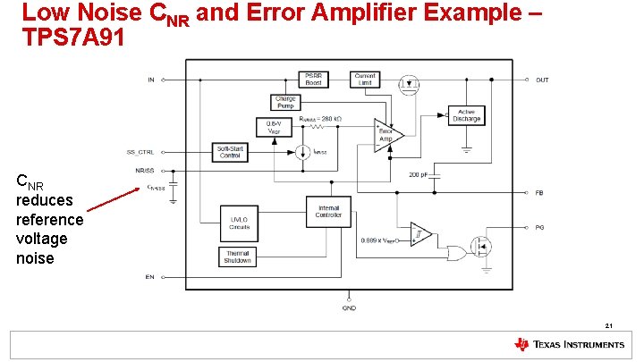
Low Noise CNR and Error Amplifier Example – TPS 7 A 91 CNR reduces reference voltage noise 21

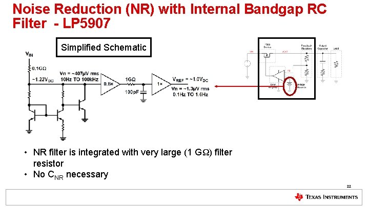
Noise Reduction (NR) with Internal Bandgap RC Filter - LP 5907 Simplified Schematic • NR filter is integrated with very large (1 GΩ) filter resistor • No CNR necessary 22

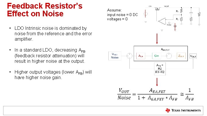
Feedback Resistor’s Effect on Noise Assume: input noise = 0 DC voltages = 0 • LDO Intrinsic noise is dominated by noise from the reference and the error amplifier. • In a standard LDO, decreasing AFB (feedback resistor attenuation) will result in higher noise at the output. • Higher output voltages (lower AFB) will have higher noise gain.

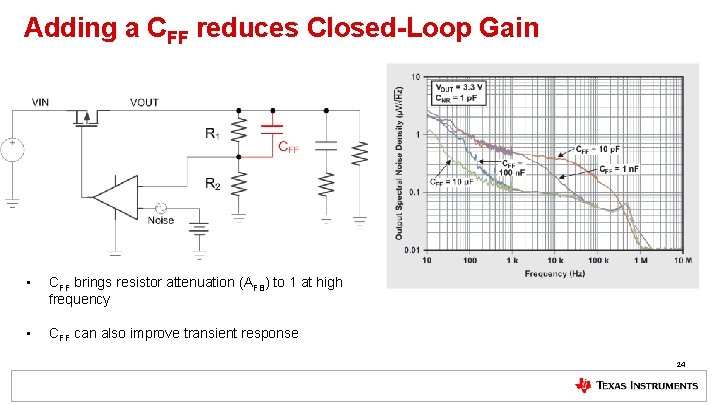
Adding a CFF reduces Closed-Loop Gain • CFF brings resistor attenuation (AFB) to 1 at high frequency • CFF can also improve transient response 24

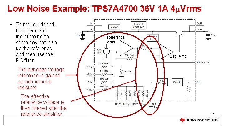
Low Noise Example: TPS 7 A 4700 36 V 1 A 4 Vrms • To reduce closedloop gain, and therefore noise, some devices gain up the reference, and then use the RC filter. Reference Amp Error Amp The bandgap voltage reference is gained up with internal resistors. The effective reference voltage is then filtered after the reference amplifier. 25

Overview • General Block Diagram Review • Small Signal Model • LDO Pass Devices – PMOS – NMOS – BJT • LDO Performance – – Dropout Noise PSRR Startup 26

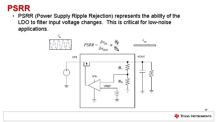
PSRR • PSRR (Power Supply Ripple Rejection) represents the ability of the LDO to filter input voltage changes. This is critical for low-noise applications. 27

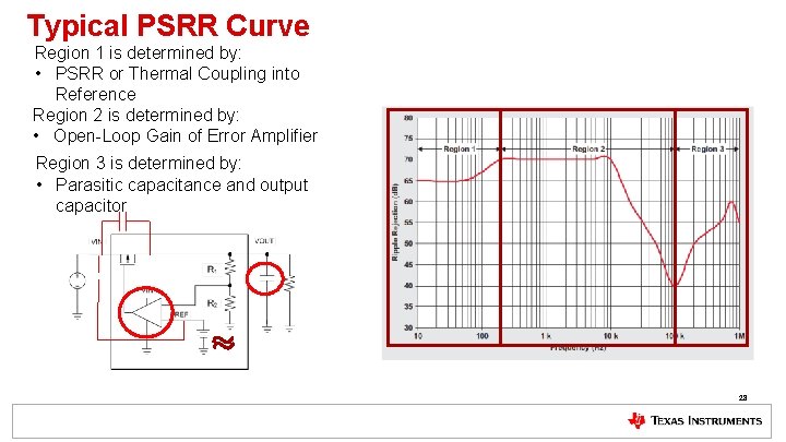
Typical PSRR Curve Region 1 is determined by: • PSRR or Thermal Coupling into Reference Region 2 is determined by: • Open-Loop Gain of Error Amplifier Region 3 is determined by: • Parasitic capacitance and output capacitor 28

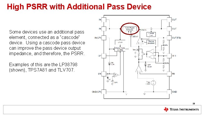
High PSRR with Additional Pass Device Some devices use an additional pass element, connected as a “cascode” device. Using a cascode pass device can improve the pass device output impedance, and therefore, the PSRR. Examples of this are the LP 38798 (shown), TPS 7 A 81 and TLV 707. 29

Overview • General Block Diagram Review • Small Signal Model • LDO Pass Devices – PMOS – NMOS – BJT • LDO Performance – – Dropout Noise PSRR Startup 30

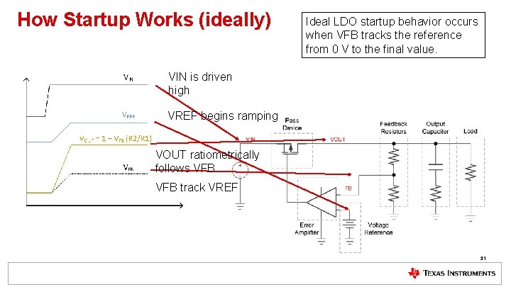
How Startup Works (ideally) Ideal LDO startup behavior occurs when VFB tracks the reference from 0 V to the final value. VIN is driven high VREF begins ramping VOUT ratiometrically follows VFB track VREF 31

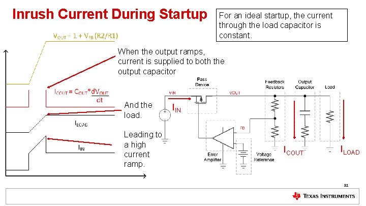
Inrush Current During Startup For an ideal startup, the current through the load capacitor is constant. When the output ramps, current is supplied to both the output capacitor And the load. Leading to a high current ramp. IIN ICOUT ILOAD 32

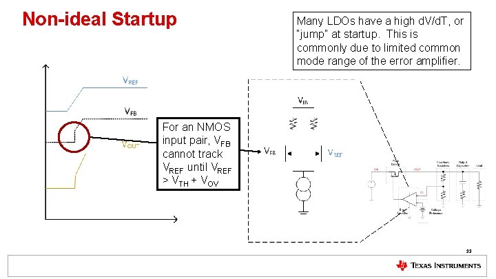
Non-ideal Startup Many LDOs have a high d. V/d. T, or “jump” at startup. This is commonly due to limited common mode range of the error amplifier. For an NMOS input pair, VFB cannot track VREF until VREF > VTH + VOV 33

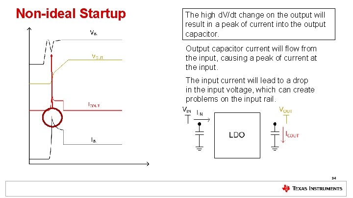
Non-ideal Startup The high d. V/dt change on the output will result in a peak of current into the output capacitor. Output capacitor current will flow from the input, causing a peak of current at the input. The input current will lead to a drop in the input voltage, which can create problems on the input rail. 34

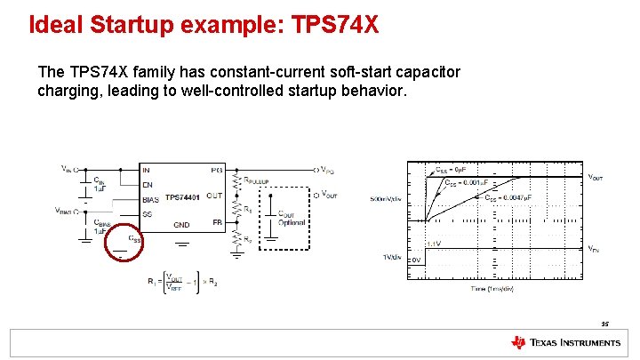
Ideal Startup example: TPS 74 X The TPS 74 X family has constant-current soft-start capacitor charging, leading to well-controlled startup behavior. 35

© Copyright 2017 Texas Instruments Incorporated. All rights reserved. This material is provided strictly “as-is, ” for informational purposes only, and without any warranty. Use of this material is subject to TI’s Terms of Use, viewable at TI. com