JRASRF Work Package 7 Power Couplers Hassen Jenhani
- Slides: 21

JRA-SRF Work Package 7 Power Couplers Hassen Jenhani (LAL) CARE’ 08, CERN, December 2008

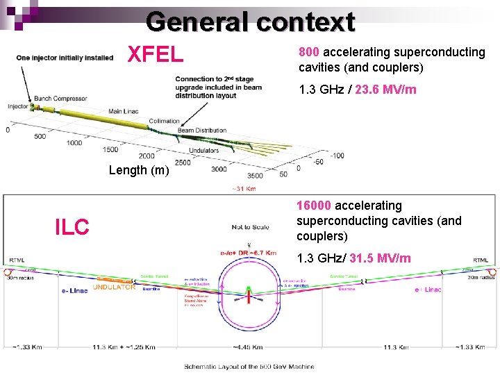
General context XFEL 800 accelerating superconducting cavities (and couplers) 1. 3 GHz / 23. 6 MV/m Length (m) ILC 16000 accelerating superconducting cavities (and couplers) 1. 3 GHz/ 31. 5 MV/m

RF conditioning All couplers need to be cleaned and tested (RF conditioning) before their assembly on the cavities Coupler RF conditioning: High RF power For XFEL: 1 MW for short pulses & 0. 5 MW for 1. 3 ms pulses For ILC: 2 MW for short pulses & 1 MW for 1. 5 ms pulses Possibility of arcs Possibility of strong vacuum bursts Strong multipacting (resonant electron avalanches) …. . RF conditioning should be: ü well mastered security for the coupler üoptimized short conditioning time Damage the coupler

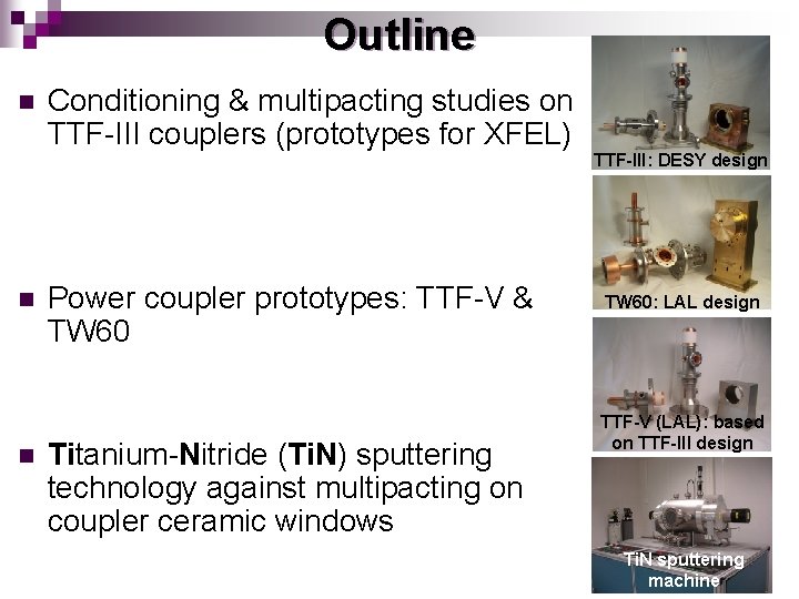
Outline n n n Conditioning & multipacting studies on TTF-III couplers (prototypes for XFEL) Power coupler prototypes: TTF-V & TW 60 Titanium-Nitride (Ti. N) sputtering technology against multipacting on coupler ceramic windows TTF-III: DESY design TW 60: LAL design TTF-V (LAL): based on TTF-III design Ti. N sputtering machine

Studies on the TTF-III couplers

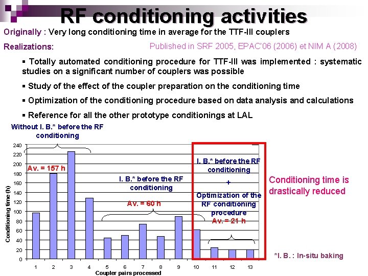
RF conditioning activities Originally : Very long conditioning time in average for the TTF-III couplers Published in SRF 2005, EPAC’ 06 (2006) et NIM A (2008) Realizations: § Totally automated conditioning procedure for TTF-III was implemented : systematic studies on a significant number of couplers was possible § Study of the effect of the coupler preparation on the conditioning time § Optimization of the conditioning procedure based on data analysis and calculations § Reference for all the other prototype conditionings at LAL Without I. B. * before the RF conditioning 240 220 200 Conditioning time (h) 180 I. B. * before the RF conditioning Av. = 157 h I. B. * before the RF conditioning 160 140 Av. = 60 h 120 100 80 + Optimization of the RF conditioning procedure Av. = 21 h Conditioning time is drastically reduced 60 40 20 *I. B. : In-situ baking 0 1 2 3 4 5 6 7 8 Coupler pairs processed 9 10 11 12 13

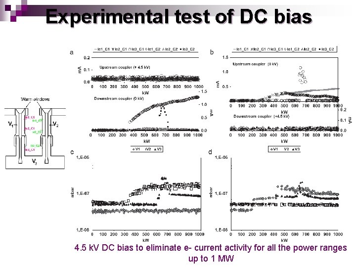
Experimental test of DC bias 4. 5 k. V DC bias to eliminate e- current activity for all the power ranges up to 1 MW

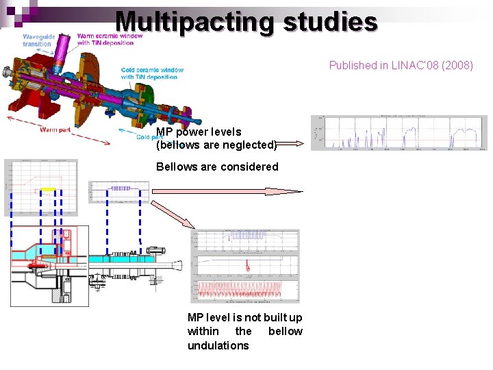
Multipacting studies Published in LINAC’ 08 (2008) MP power levels (bellows are neglected) Bellows are considered MP level is not built up within the bellow undulations Comparison between MP simulation and e- current measurements

New prototype couplers: TTFV &TW 60

Need for prototypes TTF-III is the baseline coupler for the ILC: ü Well known coupler ü Tested on high performance TESLA cavities (35 MV/m) ü Short conditioning time But: ü Complex geometry ü Expensive Two axes for prototypes were investigated at LAL : § Similar coupler with best performances: TTF-V power coupler § New coupler design with simpler geometry: TW 60 power coupler Two coupler pairs of each model were designed, ordered and received at LAL. Only one pair of each model was already tested using the TTF-III coupler conditioning procedure

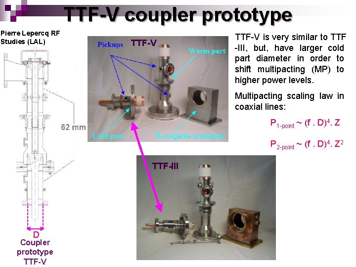
TTF-V coupler prototype Pierre Lepercq RF Studies (LAL) TTF-V is very similar to TTF -III, but, have larger cold part diameter in order to shift multipacting (MP) to higher power levels. Multipacting scaling law in coaxial lines: P 1 -point ~ (f. D)4. Z P 2 -point ~ (f. D)4. Z 2 TTF-III D Coupler prototype TTF-V

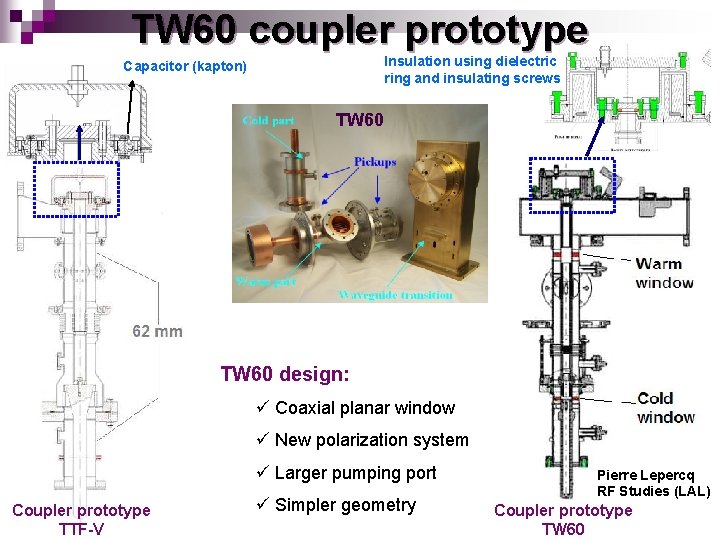
TW 60 coupler prototype Insulation using dielectric ring and insulating screws Capacitor (kapton) TW 60 design: ü Coaxial planar window ü New polarization system ü Larger pumping port Coupler prototype TTF-V ü Simpler geometry Pierre Lepercq RF Studies (LAL) Coupler prototype TW 60

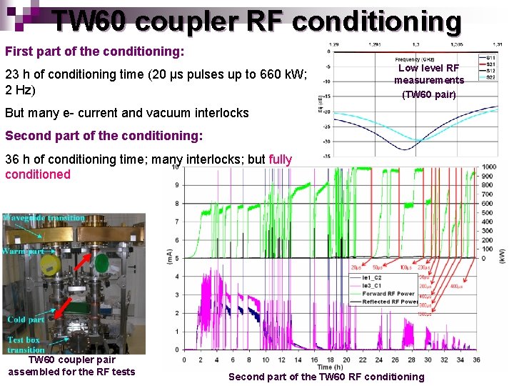
TW 60 coupler RF conditioning First part of the conditioning: 23 h of conditioning time (20 µs pulses up to 660 k. W; 2 Hz) Low level RF measurements (TW 60 pair) But many e- current and vacuum interlocks Second part of the conditioning: 36 h of conditioning time; many interlocks; but fully conditioned TW 60 coupler pair assembled for the RF tests Second part of the TW 60 RF conditioning

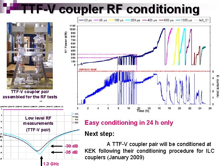
TTF-V coupler RF conditioning TTF-V RF conditioning Published in LINAC’ 08 (2008) TTF-V coupler pair assembled for the RF tests Frequency (GHz) Low level RF measurements (TTF-V pair) Easy conditioning in 24 h only Next step: d. B) -30 d. B -35 d. B 1. 3 GHz A TTF-V coupler pair will be conditioned at KEK following their conditioning procedure for ILC couplers (January 2009)

Titanium-nitride coating activity for the coupler ceramic windows

Objective Nanometric Titanium-Nitride (Ti. N) layer is needed to be deposed on the coupler RF windows to avoid harmful multipacting. Only few laboratories and industries master this technology. Our aims: § mastery of Ti. N sputtering technology § optimization of the deposition process § obtaining good surface behavior against MP § and study of the MP process using the produced samples with well known surface characteristics

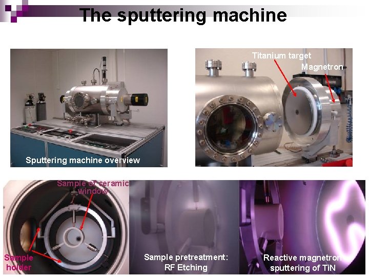
The sputtering machine Titanium target Magnetron Sputtering machine overview Sample of ceramic window Sample holder Sample pretreatment: RF Etching Reactive magnetron sputtering of Ti. N

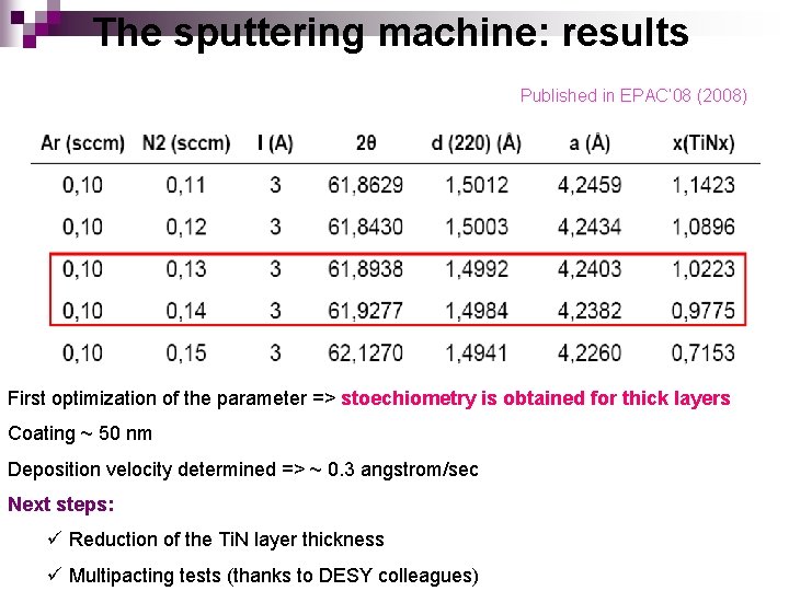
The sputtering machine: results Published in EPAC’ 08 (2008) First optimization of the parameter => stoechiometry is obtained for thick layers Coating ~ 50 nm Deposition velocity determined => ~ 0. 3 angstrom/sec Next steps: ü Reduction of the Ti. N layer thickness ü Multipacting tests (thanks to DESY colleagues)

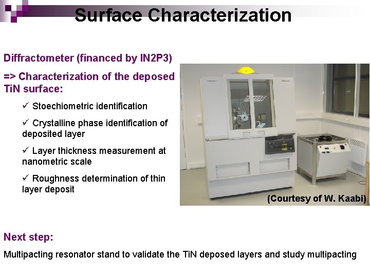
Surface Characterization Diffractometer (financed by IN 2 P 3) => Characterization of the deposed Ti. N surface: ü Stoechiometric identification ü Crystalline phase identification of deposited layer ü Layer thickness measurement at nanometric scale ü Roughness determination of thin layer deposit (Courtesy of W. Kaabi) Next step: Multipacting resonator stand to validate the Ti. N deposed layers and study multipacting

Summary CARE support had a strong impact on the coupler activities at LAL: n Drastic reduction of the conditioning time of the TTF-III couplers was achieved: very good result for the XFEL and ILC. n Good expertise in RF power couplers was acquired at LAL: LAL in charge of XFEL couplers industrialization. n Two coupler prototypes TTF-V and TW 60 (alternatives for the ILC baseline coupler) were designed at LAL. RF conditioning was successful and more tests are planned. n Ti. N deposition activity is effective at LAL: first results are fully satisfactory & local surface characterization facility is growing with the participation of the IN 2 P 3 (funds for the diffractometer)

Acknowledgment Thanks to J. Bastide, S. Cavalier, F. Cordillot, T. Chabaud, L. Grandsire, T. Garvey, W. Kaabi, M. Lacroix, P. Lepercq, B. Mercier, M. Omeich, C. Prévost, Yann Peinaud, A. Thiebault, A. Variola and J. Vieira from LAL. Thanks to our DESY colleagues especially A. Brinkmann, S. Choroba, D. Kostin, W-D. Möller and D. Proch. Thanks to G. Keppel, V. Palmieri and F. Strada from INFN/LNL We acknowledge the support of the European Community-Research Infrastructure Activity under the FP 6 ‘‘Structuring the European Research Area’’ programme (CARE, Contract no. RII 3 -CT-2003 -506395).