FCC Week Amsterdam April 9 13 2018 Overview
- Slides: 21

FCC Week - Amsterdam, April 9 -13, 2018 Overview of Conductor R&D at Fermilab Emanuela Barzi US Magnet Development Program Fermi National Accelerator Laboratory

Outline • Jc increase: • Motivation • Nb 3 Sn (traditional) HT optimization • Artificial Pinning Centers • High-Cp: • Motivation • Demonstration (FNAL/Hypertech) • Industrialization (FNAL/B-OST+B-EAS) • Improve Ic retention (stress/strain sensitivity): • Motivation • Nb 3 Al • Nb 3 Sn • HTS E. Barzi, Overview of Conductor R&D at Fermilab, FCC 2018 o Second level 2

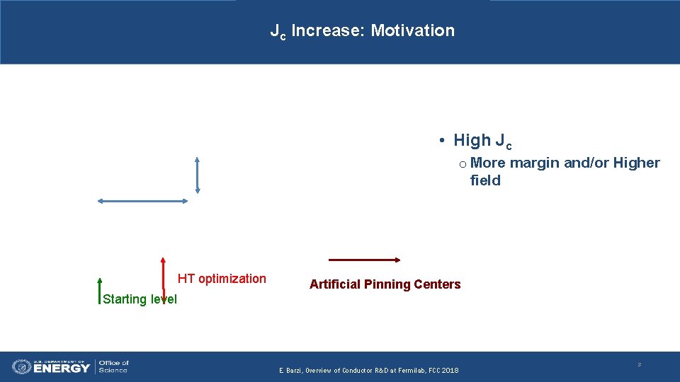
Jc Increase: Motivation • High Jc o More margin and/or Higher field HT optimization Artificial Pinning Centers Starting level E. Barzi, Overview of Conductor R&D at Fermilab, FCC 2018 o Second level 3

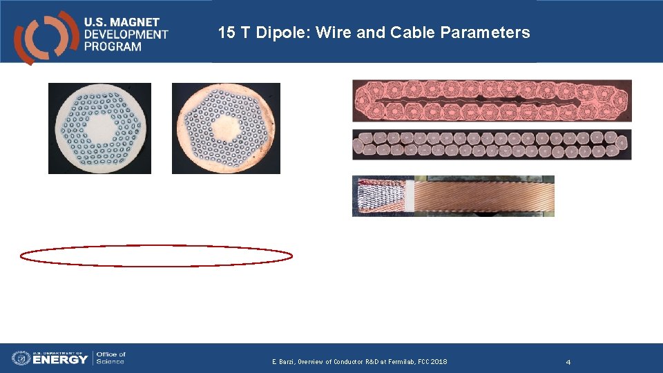
15 T Dipole: Wire and Cable Parameters E. Barzi, Overview of Conductor R&D at Fermilab, FCC 2018 4

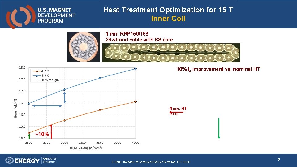
Heat Treatment Optimization for 15 T Inner Coil 1 mm RRP 150/169 28 -strand cable with SS core 10% Ic improvement vs. nominal HT Nom. HT Ave. ~10% E. Barzi, Overview of Conductor R&D at Fermilab, FCC 2018 o Second level 5

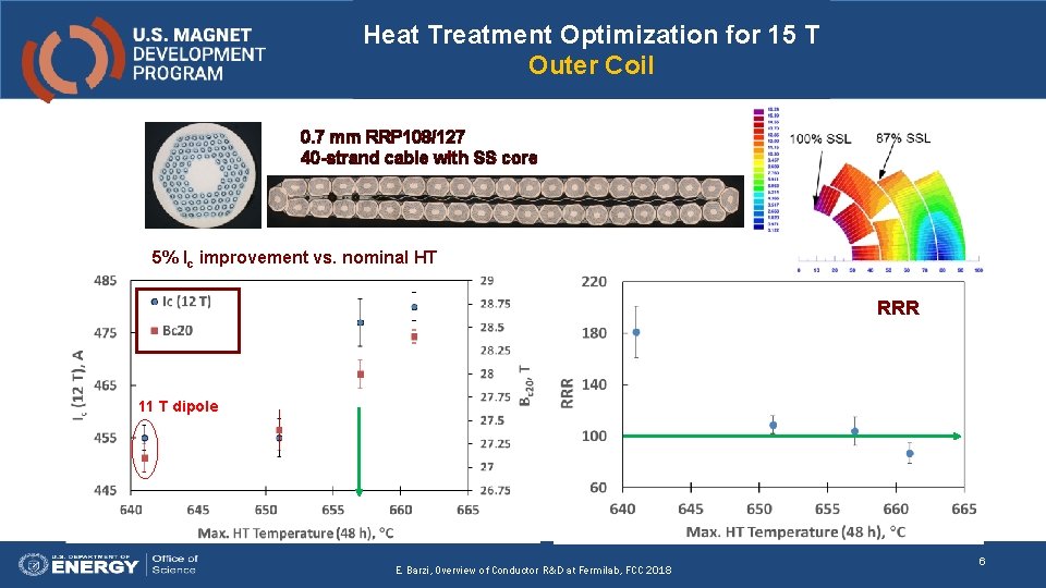
Heat Treatment Optimization for 15 T Outer Coil 0. 7 mm RRP 108/127 40 -strand cable with SS core 5% Ic improvement vs. nominal HT RRR 11 T dipole E. Barzi, Overview of Conductor R&D at Fermilab, FCC 2018 o Second level 6

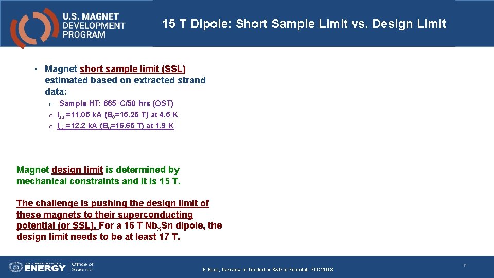
15 T Dipole: Short Sample Limit vs. Design Limit • Magnet short sample limit (SSL) estimated based on extracted strand data: o Sample HT: 665 o. C/50 hrs (OST) o Issl=11. 05 k. A (B 0=15. 25 T) at 4. 5 K o Issl=12. 2 k. A (B 0=16. 65 T) at 1. 9 K Magnet design limit is determined by mechanical constraints and it is 15 T. The challenge is pushing the design limit of these magnets to their superconducting potential (or SSL). For a 16 T Nb 3 Sn dipole, the design limit needs to be at least 17 T. E. Barzi, Overview of Conductor R&D at Fermilab, FCC 2018 7

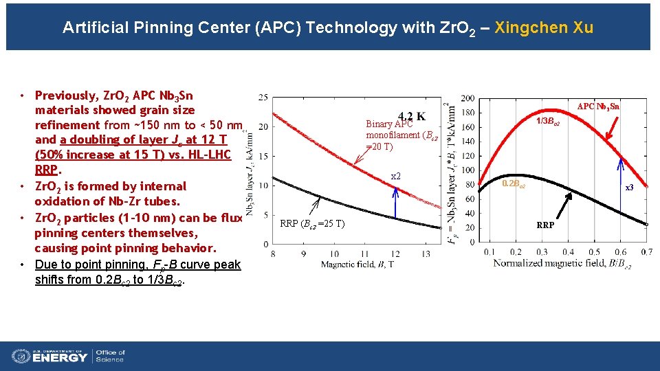
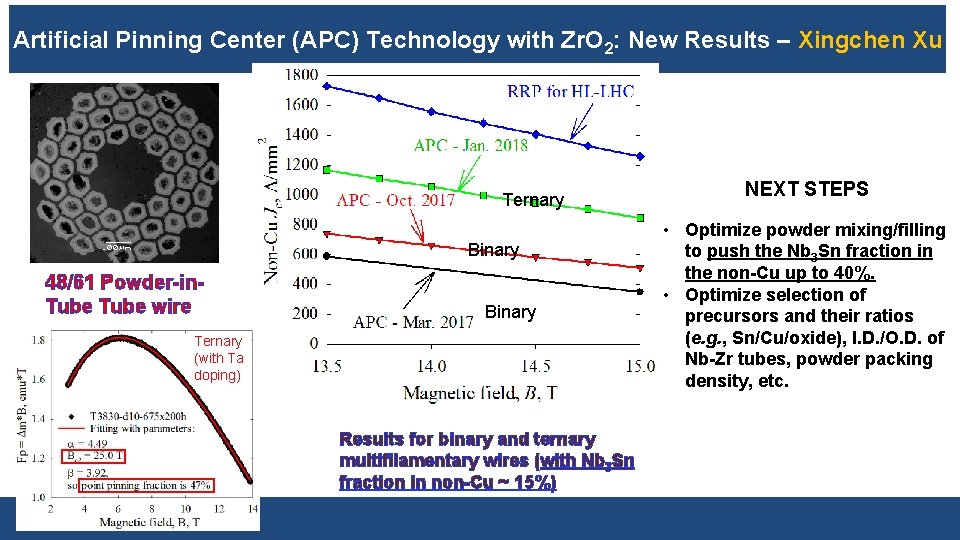
Artificial Pinning Center (APC) Technology with Zr. O 2 – Xingchen Xu • Previously, Zr. O 2 APC Nb 3 Sn materials showed grain size refinement from ~150 nm to < 50 nm and a doubling of layer Jc at 12 T (50% increase at 15 T) vs. HL-LHC RRP. • Zr. O 2 is formed by internal oxidation of Nb-Zr tubes. • Zr. O 2 particles (1 -10 nm) can be flux pinning centers themselves, causing point pinning behavior. • Due to point pinning, Fp-B curve peak shifts from 0. 2 Bc 2 to 1/3 Bc 2. 8 APC Nb 3 Sn 1/3 Bc 2 Binary APC monofilament (Bc 2 =20 T) x 2 RRP (Bc 2 =25 T) 0. 2 Bc 2 x 3 RRP

Artificial Pinning Center (APC) Technology with Zr. O 2: New Results – Xingchen Xu Ternary Binary 48/61 Powder-in. Tube wire Binary Ternary (with Ta doping) Results for binary and ternary multifilamentary wires (with Nb 3 Sn fraction in non-Cu ~ 15%) 9 NEXT STEPS • Optimize powder mixing/filling to push the Nb 3 Sn fraction in the non-Cu up to 40%. • Optimize selection of precursors and their ratios (e. g. , Sn/Cu/oxide), I. D. /O. D. of Nb-Zr tubes, powder packing density, etc.

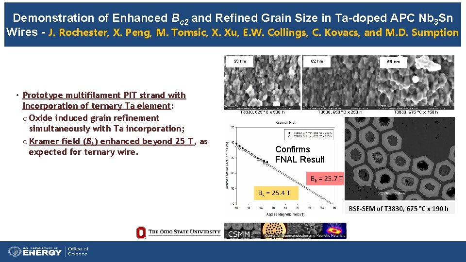
Demonstration of Enhanced Bc 2 and Refined Grain Size in Ta-doped APC Nb 3 Sn Wires - J. Rochester, X. Peng, M. Tomsic, X. Xu, E. W. Collings, C. Kovacs, and M. D. Sumption 62 nm 53 nm • Prototype multifilament PIT strand with incorporation of ternary Ta element: o Oxide induced grain refinement simultaneously with Ta incorporation; o Kramer field (Bk) enhanced beyond 25 T, as expected for ternary wire. 10 T 3830, 625 °C x 500 h T 3830, 650 °C x 250 h Confirms FNAL Result 68 nm T 3830, 675 °C x 150 h

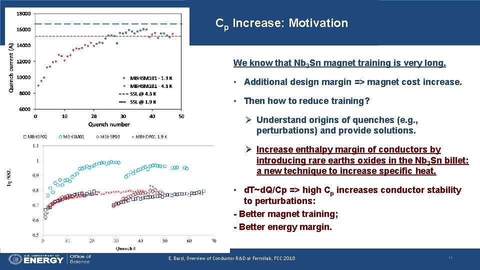
Cp Increase: Motivation We know that Nb 3 Sn magnet training is very long. • Additional design margin => magnet cost increase. • Then how to reduce training? Ø Understand origins of quenches (e. g. , perturbations) and provide solutions. Ø Increase enthalpy margin of conductors by introducing rare earths oxides in the Nb 3 Sn billet: a new technique to increase specific heat. • d. T~d. Q/Cp => high Cp increases conductor stability to perturbations: - Better magnet training; - Better energy margin. E. Barzi, Overview of Conductor R&D at Fermilab, FCC 2018 11

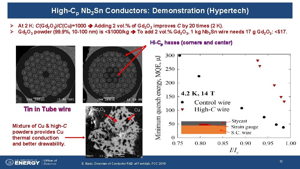
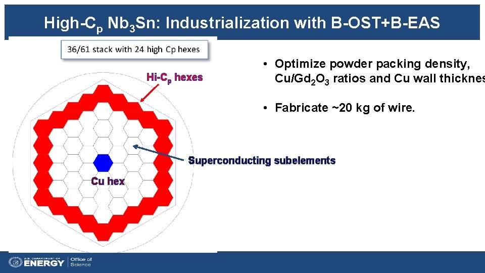
High-Cp Nb 3 Sn Conductors: Demonstration (Hypertech) Ø At 2 K: C(Gd 2 O 3)/C(Cu)=1000 Adding 2 vol. % of Gd 2 O 3 improves C by 20 times (2 K). Ø Gd 2 O 3 powder (99. 9%, 10 -100 nm) is <$1000/kg To add 2 vol. % Gd 2 O 3, 1 kg Nb 3 Sn wire needs 17 g Gd 2 O 3: <$17. Hi-Cp hexes (corners and center) Tin in Tube wire Gd 2 O 3 Cu Mixture of Cu & high-C powders provides Cu thermal conduction and better drawability. E. Barzi, Overview of Conductor R&D at Fermilab, FCC 2018 12

High-Cp Nb 3 Sn: Industrialization with B-OST+B-EAS Hi-Cp hexes • Optimize powder packing density, Cu/Gd 2 O 3 ratios and Cu wall thicknes • Fabricate ~20 kg of wire. Superconducting subelements Cu hex

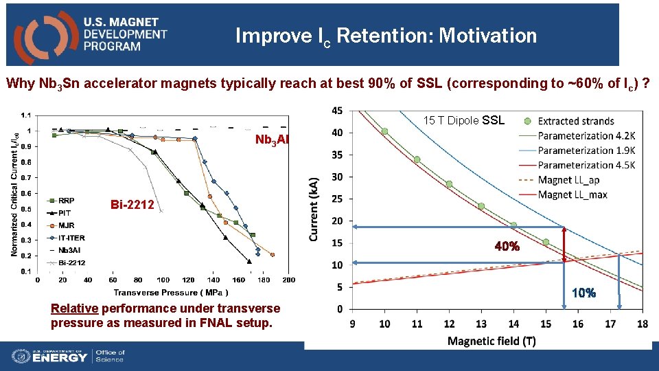
Improve Ic Retention: Motivation Why Nb 3 Sn accelerator magnets typically reach at best 90% of SSL (corresponding to ~60% of Ic) ? 15 T Dipole SSL Nb 3 Al Bi-2212 40% 10% Relative performance under transverse pressure as measured in FNAL setup. 14

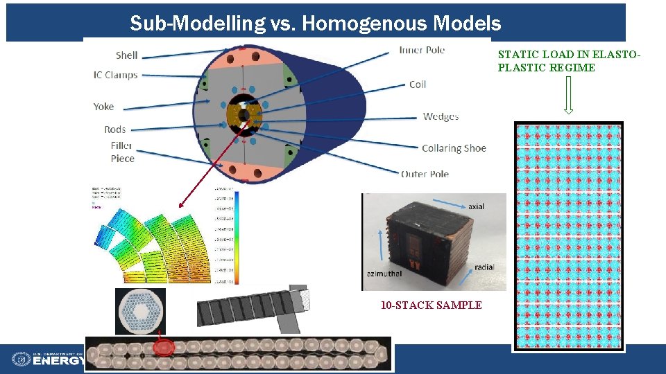
Sub-Modelling vs. Homogenous Models STATIC LOAD IN ELASTOPLASTIC REGIME Four magnetic cryostats with up to 15 T/17 T background field, and with cold apertures between 64 mm and 147 mm are connected to new vent and vacuum systems. 10 -STACK SAMPLE 15

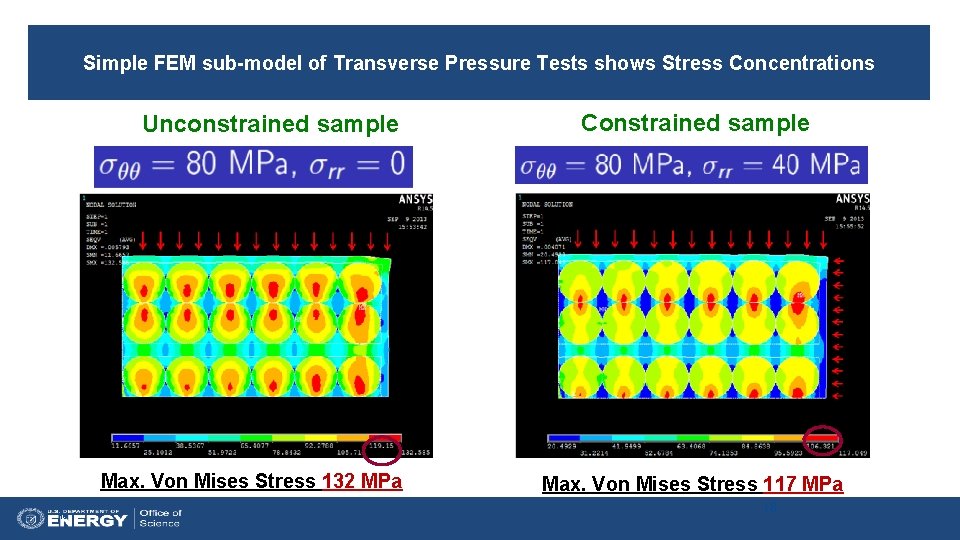
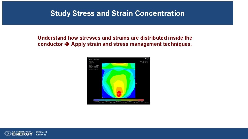
Simple FEM sub-model of Transverse Pressure Tests shows Stress Concentrations Unconstrained sample Max. Von Mises Stress 132 MPa 16 Constrained sample Max. Von Mises Stress 117 MPa 16

Study Stress and Strain Concentration Understand how stresses and strains are distributed inside the conductor Apply strain and stress management techniques. 17

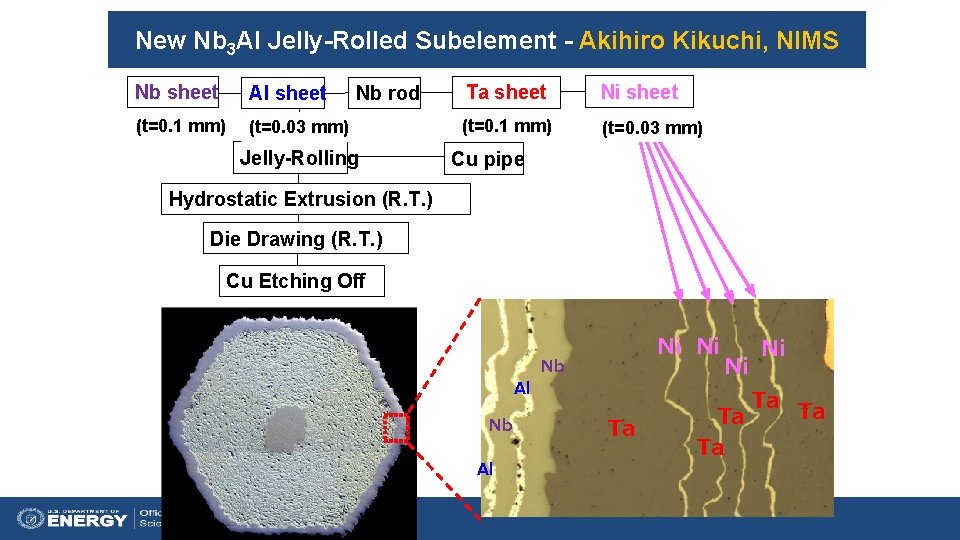
New Nb 3 Al Jelly-Rolled Subelement - Akihiro Kikuchi, NIMS Nb sheet Al sheet (t=0. 1 mm) (t=0. 03 mm) Nb rod Jelly-Rolling Ta sheet Ni sheet (t=0. 1 mm) (t=0. 03 mm) Cu pipe Hydrostatic Extrusion (R. T. ) Die Drawing (R. T. ) Cu Etching Off Al Nb Al Ni Ni Nb Ta Ni Ni Ta Ta

Jelly Roll Nb 3 Al Performance vs HL-LHC and FCC Specs

Conclusions • SC wire and cable R&D for the 15 T Dipole demonstrator: o Cables were designed and optimized based on the properties of present Nb 3 Sn wires. o Sensitivities studies to heat treatment were performed to push performance to nominal required. o Next: Sub-modelling studies to identify stress and strain concentration areas. • R&D on next generation Nb 3 Sn wires with high Jc and high Cp for accelerator magnets is a must: o Improving Jc using Artificial Pinning Centers supported by several sources o Improving Cp by adding high-Cp substances supported by FNAL GARD. • Support of strain resistant Nb 3 Al by NIMS would reduce risk in case strain management solutions fail. E. Barzi, Overview of Conductor R&D at Fermilab, FCC 2018 o Second level 20

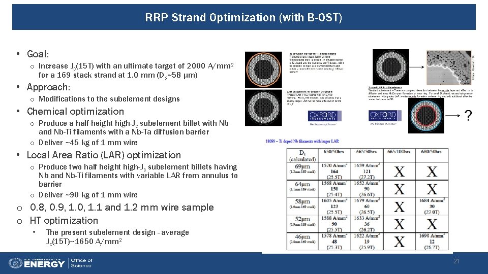
RRP Strand Optimization (with B-OST) • Goal: o Increase Jc(15 T) with an ultimate target of 2000 A/mm 2 for a 169 stack strand at 1. 0 mm (Ds~58 µm) • Approach: o Modifications to the subelement designs • Chemical optimization o Produce a half height high-Jc subelement billet with Nb and Nb-Ti filaments with a Nb-Ta diffusion barrier o Deliver ~45 kg of 1 mm wire • Local Area Ratio (LAR) optimization o Produce two half height high-Jc subelement billets having Nb and Nb-Ti filaments with variable LAR from annulus to barrier o Deliver ~90 kg of 1 mm wire o 0. 8, 0. 9, 1. 0, 1. 1 and 1. 2 mm wire sample o HT optimization • The present subelement design - average Jc(15 T)~1650 A/mm 2 21