ENR 116 Engineering Materials Module 4 Nonmetals Dr


- Slides: 24

ENR 116 Engineering Materials Module 4 Non-metals Dr David Steele

Copyright Notice Do not remove this notice. COMMMONWEALTH OF AUSTRALIA Copyright Regulations 1969 WARNING This material has been produced and communicated to you by or on behalf of the University of South Australia pursuant to Part VB of the Copyright Act 1968 (the Act). The material in this communication may be subject to copyright under the Act. Any further reproduction or communication of this material by you may be the subject of copyright protection under the Act. Do not remove this notice.

Semiconductors Week 12 C

Intended Learning Outcomes At the end of this section, students will be able to: - • Describe the electronic band structure present in materials. • Understand the importance of electrons and holes in semiconductors.

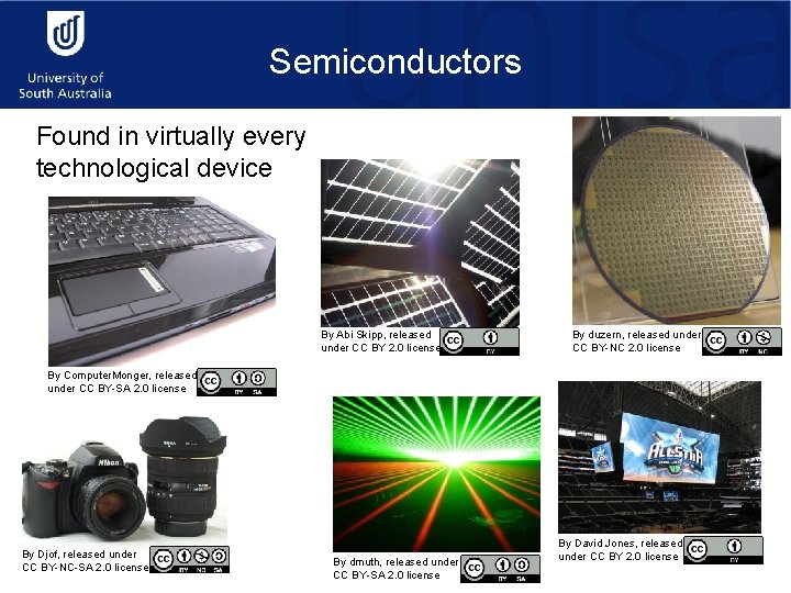
Semiconductors Found in virtually every technological device By Abi Skipp, released under CC BY 2. 0 license By duzern, released under CC BY-NC 2. 0 license By Computer. Monger, released under CC BY-SA 2. 0 license By Djof, released under CC BY-NC-SA 2. 0 license By dmuth, released under CC BY-SA 2. 0 license By David Jones, released under CC BY 2. 0 license

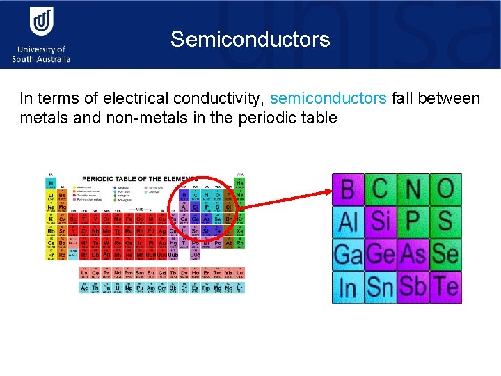
Semiconductors In terms of electrical conductivity, semiconductors fall between metals and non-metals in the periodic table

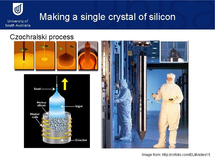
Making a single crystal of silicon Czochralski process Image from: http: //cnfolio. com/ELMnotes 15

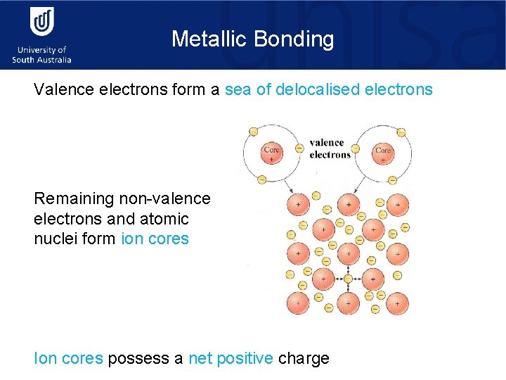
Metallic Bonding Valence electrons form a sea of delocalised electrons Remaining non-valence electrons and atomic nuclei form ion cores Ion cores possess a net positive charge

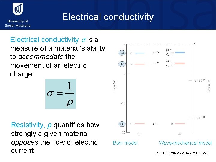
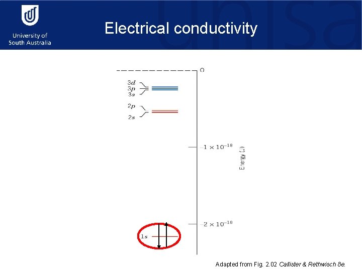
Electrical conductivity is a measure of a material's ability to accommodate the movement of an electric charge Resistivity, ρ quantifies how strongly a given material opposes the flow of electric current. Bohr model Wave-mechanical model Fig. 2. 02 Callister & Rethwisch 8 e.

Electrical conductivity Adapted from Fig. 2. 02 Callister & Rethwisch 8 e.

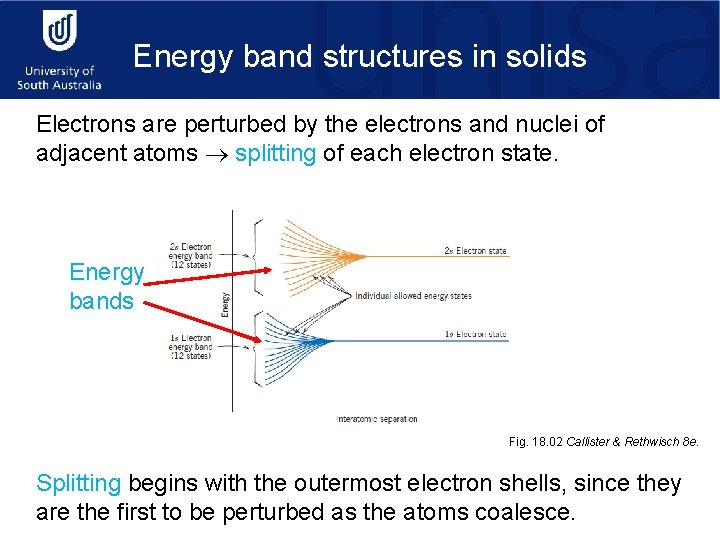
Energy band structures in solids Electrons are perturbed by the electrons and nuclei of adjacent atoms splitting of each electron state. Energy bands Fig. 18. 02 Callister & Rethwisch 8 e. Splitting begins with the outermost electron shells, since they are the first to be perturbed as the atoms coalesce.

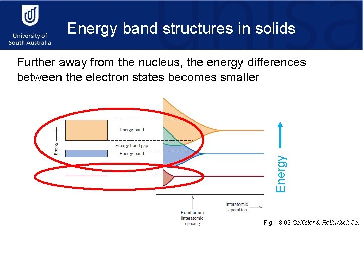
Energy band structures in solids Energy Further away from the nucleus, the energy differences between the electron states becomes smaller Fig. 18. 03 Callister & Rethwisch 8 e.

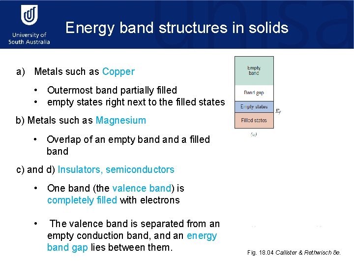
Energy band structures in solids a) Metals such as Copper • Outermost band partially filled • empty states right next to the filled states b) Metals such as Magnesium • Overlap of an empty band a filled band c) and d) Insulators, semiconductors Ef • One band (the valence band) is completely filled with electrons • The valence band is separated from an empty conduction band, and an energy band gap lies between them. Fig. 18. 04 Callister & Rethwisch 8 e.

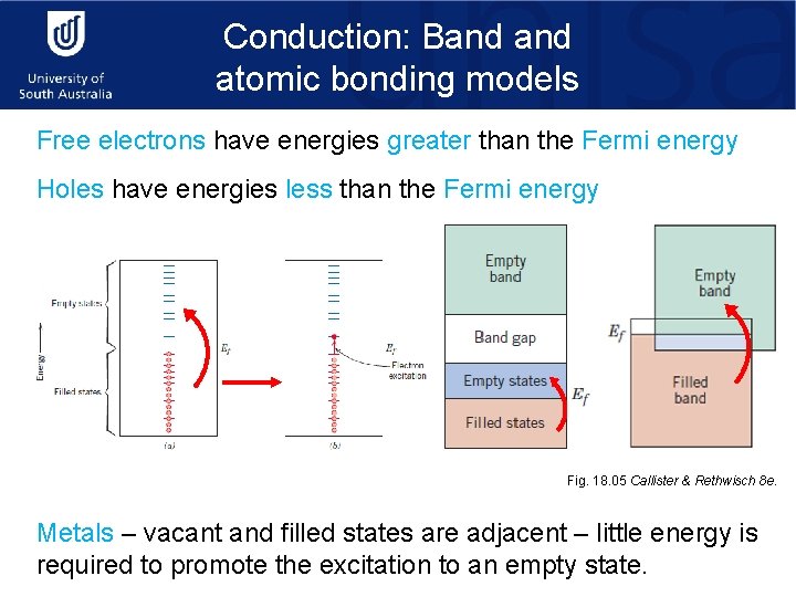
Conduction: Band atomic bonding models Free electrons have energies greater than the Fermi energy Holes have energies less than the Fermi energy Fig. 18. 05 Callister & Rethwisch 8 e. Metals – vacant and filled states are adjacent – little energy is required to promote the excitation to an empty state.

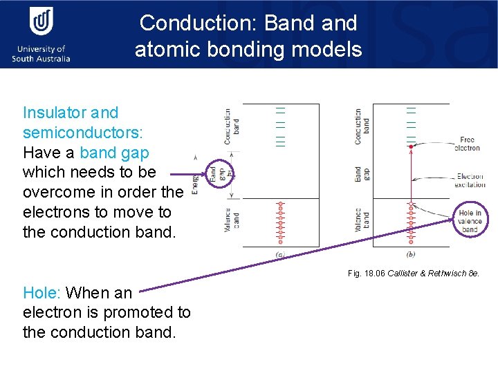
Conduction: Band atomic bonding models Insulator and semiconductors: Have a band gap which needs to be overcome in order the electrons to move to the conduction band. Fig. 18. 06 Callister & Rethwisch 8 e. Hole: When an electron is promoted to the conduction band.

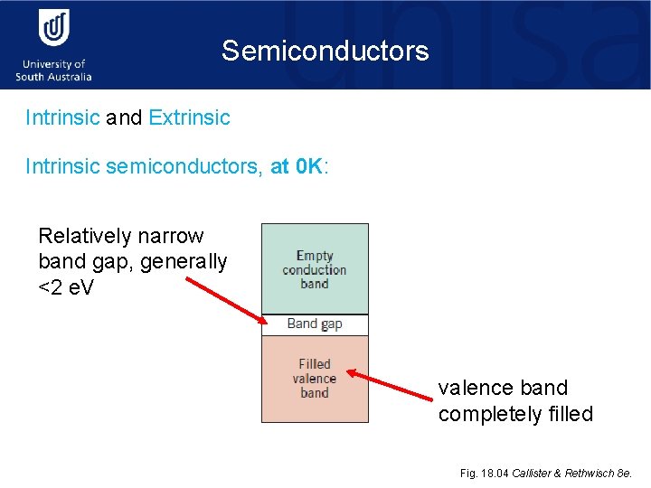
Semiconductors Intrinsic and Extrinsic Intrinsic semiconductors, at 0 K: Relatively narrow band gap, generally <2 e. V • Si • Ge • • Ga. AS In. Sb Cd. S Zn. Te valence band completely filled Fig. 18. 04 Callister & Rethwisch 8 e.

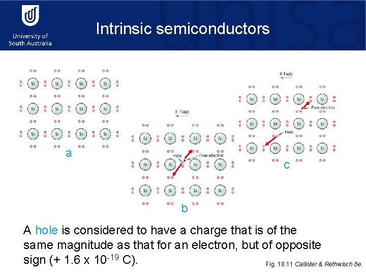
Intrinsic semiconductors a c b A hole is considered to have a charge that is of the same magnitude as that for an electron, but of opposite sign (+ 1. 6 x 10 -19 C). Fig. 18. 11 Callister & Rethwisch 8 e.

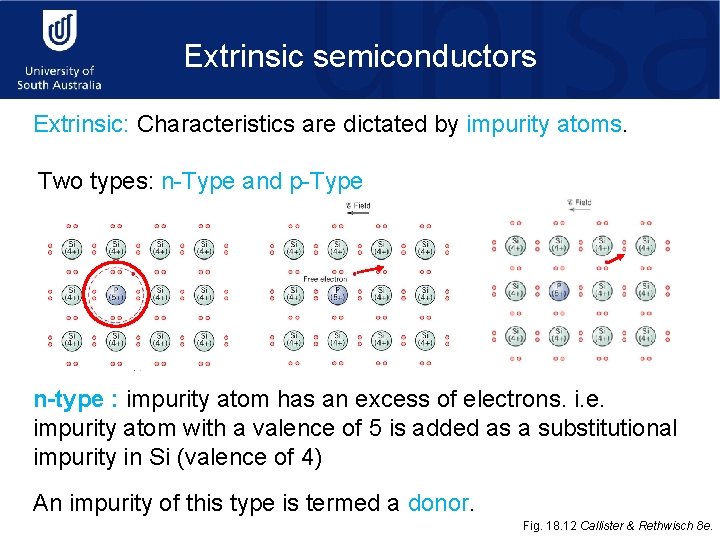
Extrinsic semiconductors Extrinsic: Characteristics are dictated by impurity atoms. Two types: n-Type and p-Type n-type : impurity atom has an excess of electrons. i. e. impurity atom with a valence of 5 is added as a substitutional impurity in Si (valence of 4) An impurity of this type is termed a donor. Fig. 18. 12 Callister & Rethwisch 8 e.

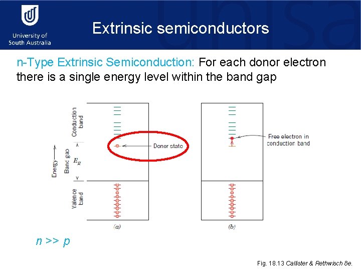
Extrinsic semiconductors n-Type Extrinsic Semiconduction: For each donor electron there is a single energy level within the band gap n >> p Fig. 18. 13 Callister & Rethwisch 8 e.

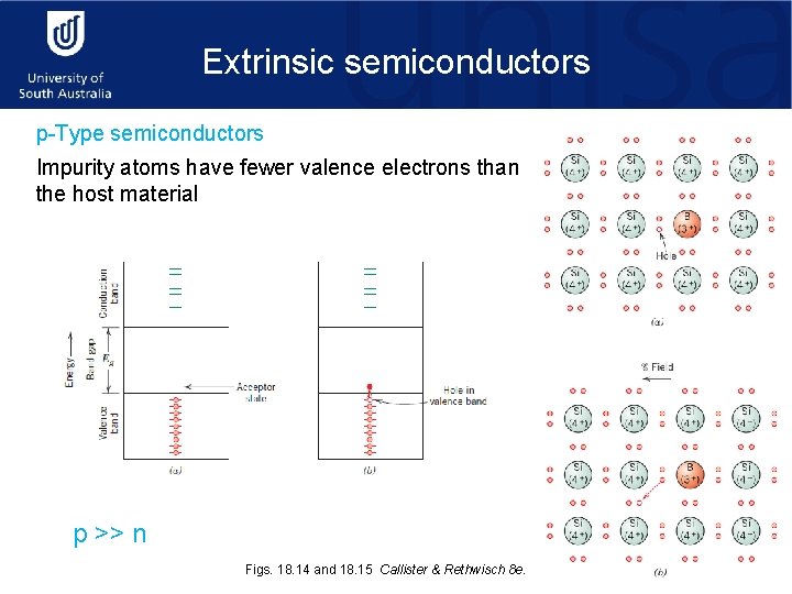
Extrinsic semiconductors p-Type semiconductors Impurity atoms have fewer valence electrons than the host material p >> n Figs. 18. 14 and 18. 15 Callister & Rethwisch 8 e.

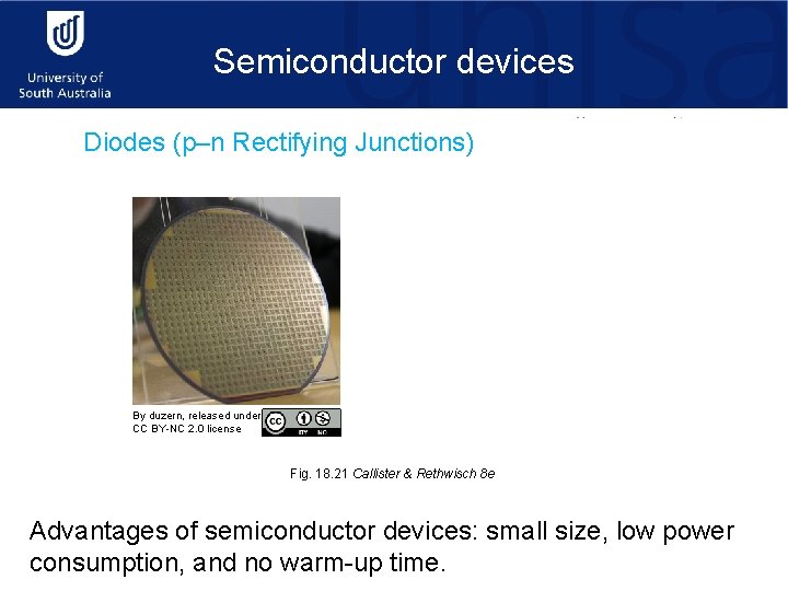
Semiconductor devices Diodes (p–n Rectifying Junctions) By duzern, released under CC BY-NC 2. 0 license Fig. 18. 21 Callister & Rethwisch 8 e. Advantages of semiconductor devices: small size, low power consumption, and no warm-up time.

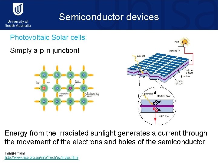
Semiconductor devices Photovoltaic Solar cells: Simply a p-n junction! Energy from the irradiated sunlight generates a current through the movement of the electrons and holes of the semiconductor Images from http: //www. rise. org. au/info/Tech/pv/index. html

Summary • The number of free electrons depends on the electronic band structure of the material. • Semiconductors can be classified as either intrinsic or extrinsic.

ENR 116 – Mod. 5 - Slide No. 24 Thank you