EMT 112 4 ANALOGUE ELECTRONICS Lecture III Class
- Slides: 25

EMT 112 / 4 ANALOGUE ELECTRONICS Lecture III Class AB Power Amplifiers 24 March 2010 1600 – 1700 DKP 2

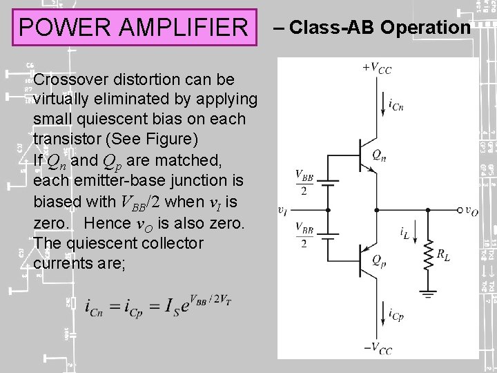
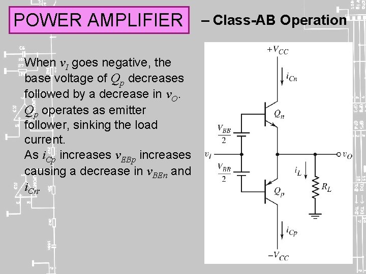
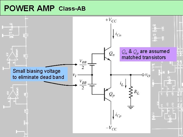
POWER AMPLIFIER Crossover distortion can be virtually eliminated by applying small quiescent bias on each transistor (See Figure) If Qn and Qp are matched, each emitter-base junction is biased with VBB/2 when v. I is zero. Hence v. O is also zero. The quiescent collector currents are; – Class-AB Operation

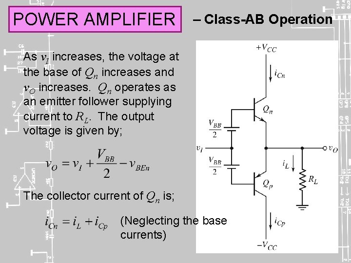
POWER AMPLIFIER – Class-AB Operation As v. I increases, the voltage at the base of Qn increases and v. O increases. Qn operates as an emitter follower supplying current to RL. The output voltage is given by; The collector current of Qn is; (Neglecting the base currents)

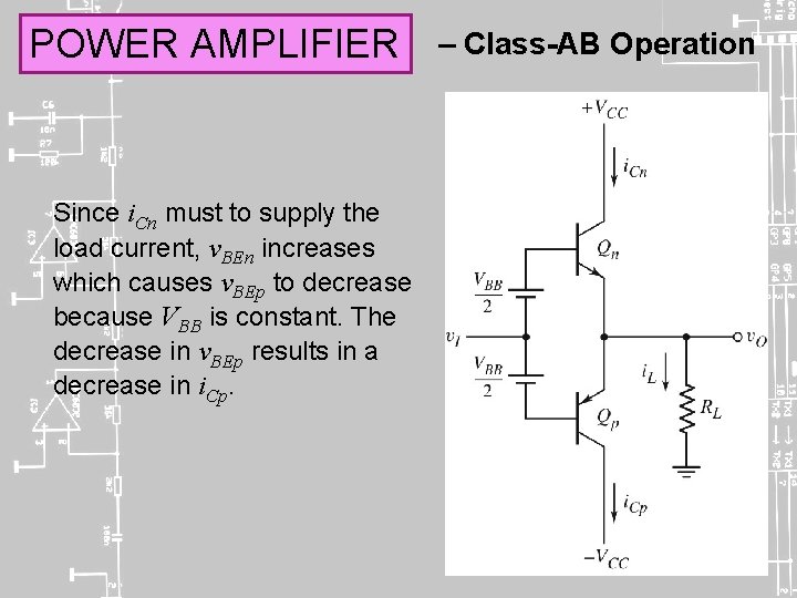
POWER AMPLIFIER Since i. Cn must to supply the load current, v. BEn increases which causes v. BEp to decrease because VBB is constant. The decrease in v. BEp results in a decrease in i. Cp. – Class-AB Operation

POWER AMPLIFIER When v. I goes negative, the base voltage of Qp decreases followed by a decrease in v. O. Qp operates as emitter follower, sinking the load current. As i. Cp increases v. EBp increases causing a decrease in v. BEn and i. Cn. – Class-AB Operation

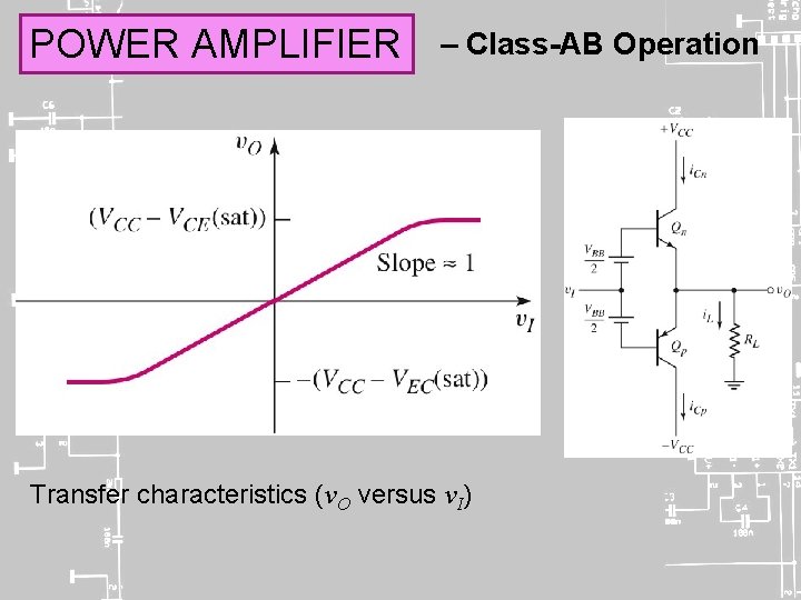
POWER AMPLIFIER – Class-AB Operation Transfer characteristics (v. O versus v. I)

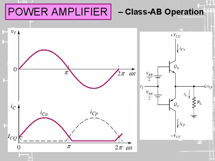
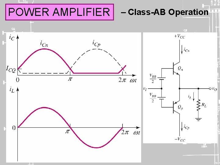
POWER AMPLIFIER – Class-AB Operation

POWER AMPLIFIER – Class-AB Operation

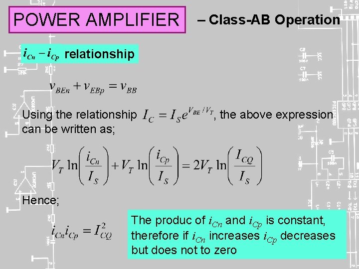
POWER AMPLIFIER – Class-AB Operation relationship Using the relationship can be written as; , the above expression Hence; The produc of i. Cn and i. Cp is constant, therefore if i. Cn increases i. Cp decreases but does not to zero

POWER AMP Class-AB Qn & Qp are assumed matched transistors Small biasing voltage to eliminate dead band

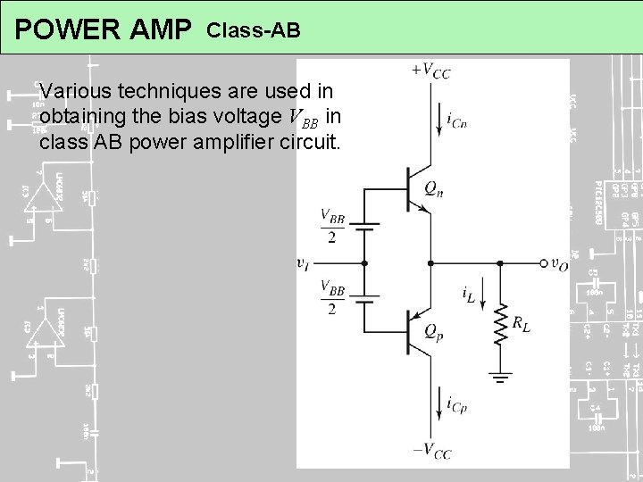
POWER AMP Class-AB Various techniques are used in obtaining the bias voltage VBB in class AB power amplifier circuit.

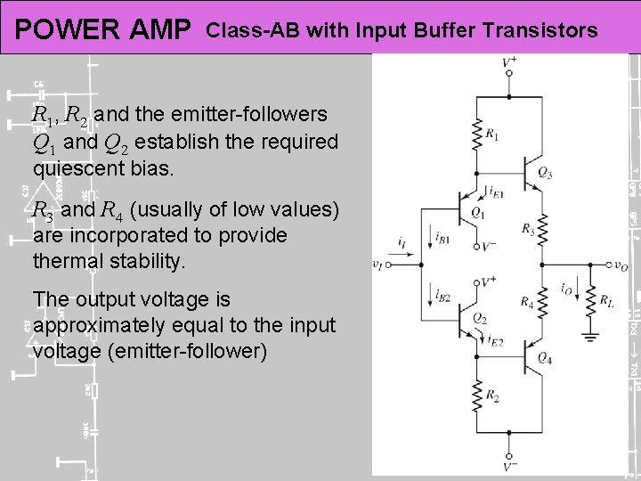
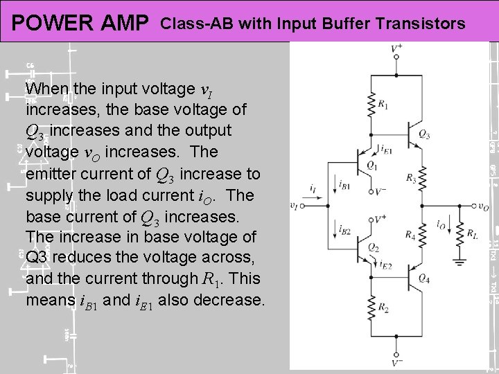
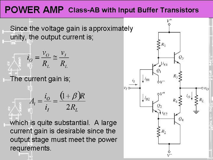
POWER AMP Class-AB with Input Buffer Transistors R 1, R 2 and the emitter-followers Q 1 and Q 2 establish the required quiescent bias. R 3 and R 4 (usually of low values) are incorporated to provide thermal stability. The output voltage is approximately equal to the input voltage (emitter-follower)

POWER AMP Class-AB with Input Buffer Transistors When the input voltage v. I increases, the base voltage of Q 3 increases and the output voltage v. O increases. The emitter current of Q 3 increase to supply the load current i. O. The base current of Q 3 increases. The increase in base voltage of Q 3 reduces the voltage across, and the current through R 1. This means i. B 1 and i. E 1 also decrease.

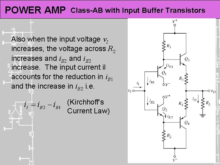
POWER AMP Class-AB with Input Buffer Transistors Also when the input voltage v. I increases, the voltage across R 2 increases and i. E 2 increase. The input current i. I accounts for the reduction in i. B 1 and the increase in i. B 2 i. e. (Kirchhoff’s Current Law)

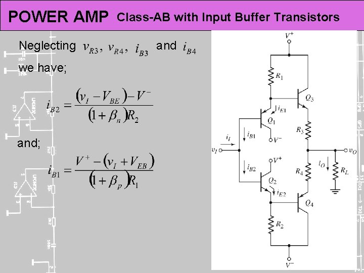
POWER AMP Neglecting we have; and; Class-AB with Input Buffer Transistors and

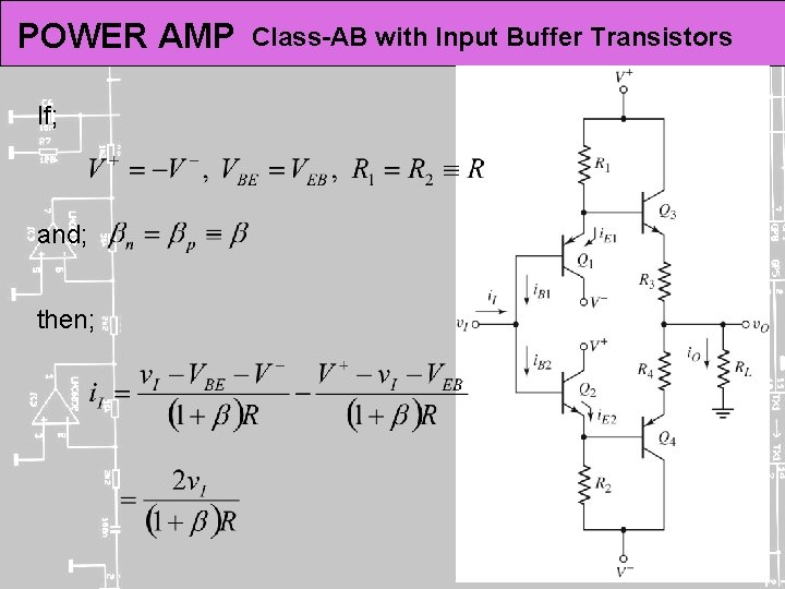
POWER AMP If; and; then; Class-AB with Input Buffer Transistors

POWER AMP Class-AB with Input Buffer Transistors Since the voltage gain is approximately unity, the output current is; The current gain is; which is quite substantial. A large current gain is desirable since the output stage must meet the power requrements.

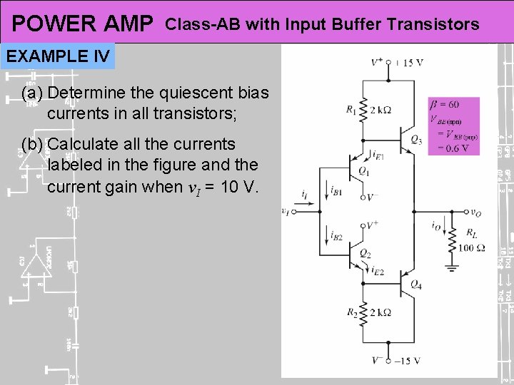
POWER AMP Class-AB with Input Buffer Transistors EXAMPLE IV (a) Determine the quiescent bias currents in all transistors; (b) Calculate all the currents labeled in the figure and the current gain when v. I = 10 V.

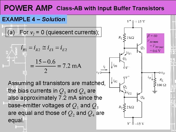
POWER AMP Class-AB with Input Buffer Transistors EXAMPLE 4 – Solution (a) For v. I = 0 (quiescent currents); Assuming all transistors are matched, the bias currents in Q 3 and Q 4 are also approximately 7. 2 m. A since the base-emitter voltages of Q 1 and Q 3 are equal and those of Q 2 and Q 4 are equal.

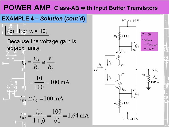
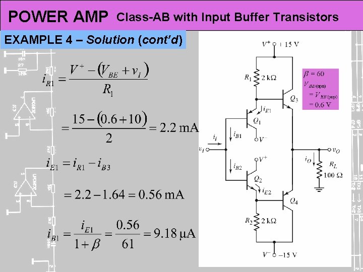
POWER AMP Class-AB with Input Buffer Transistors EXAMPLE 4 – Solution (cont’d) (b) For v. I = 10; Because the voltage gain is approx. unity;

POWER AMP Class-AB with Input Buffer Transistors EXAMPLE 4 – Solution (cont’d)

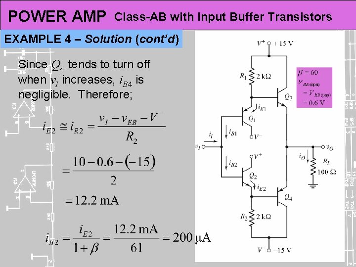
POWER AMP Class-AB with Input Buffer Transistors EXAMPLE 4 – Solution (cont’d) Since Q 4 tends to turn off when v. I increases, i. B 4 is negligible. Therefore;

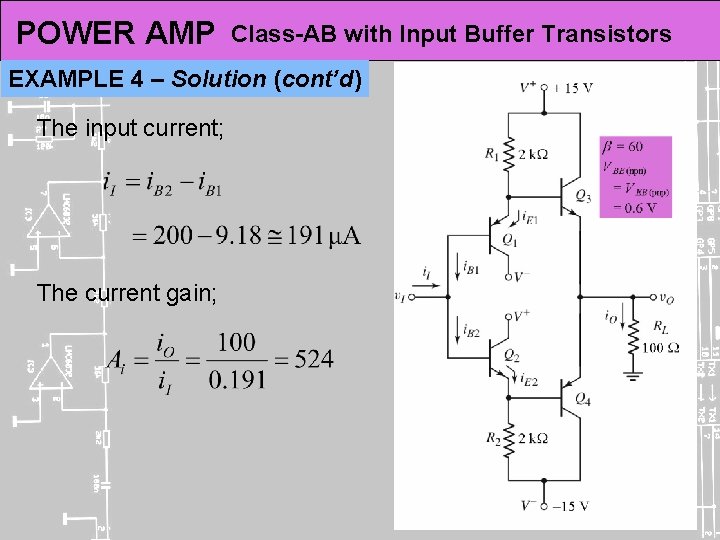
POWER AMP Class-AB with Input Buffer Transistors EXAMPLE 4 – Solution (cont’d) The input current; The current gain;

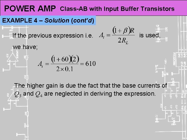
POWER AMP Class-AB with Input Buffer Transistors EXAMPLE 4 – Solution (cont’d) If the previous expression i. e. is used, we have; The higher gain is due the fact that the base currents of Q 3 and Q 4 are neglected in deriving the expression.

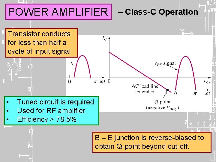
POWER AMPLIFIER – Class-C Operation Transistor conducts for less than half a cycle of input signal • • • Tuned circuit is required. Used for RF amplifier. Efficiency > 78. 5% B – E junction is reverse-biased to obtain Q-point beyond cut-off.