EMT 359 ELECTRONIC ANALOGUE II CHAPTER 2 OPAMP
- Slides: 53

EMT 359 ELECTRONIC ANALOGUE II CHAPTER 2 : OP-AMP APPLICATION & FREQUENCY RESPONSE

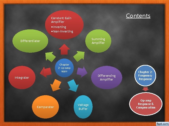
Contents Constant Gain Amplifier • Inverting • Non-inverting Summing Amplifier Differentiator Chapter 2: op-amp apps Differencing Amplifier Integrator Comparator Voltage Buffer Chapter 2: Frequency Response Op-amp Response & Compensation

Op-amp Application • Introduction Op-amps are used in many different applications. We will discuss the operation of the fundamental op-amp applications. • Keep in mind that the basic operation and characteristics of the op-amps do not change — the only thing that changes is how we use them

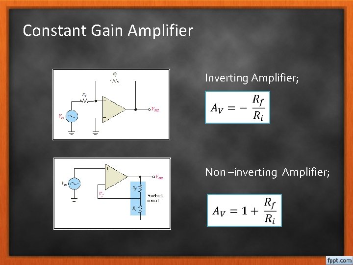
Constant Gain Amplifier Inverting Amplifier; Non –inverting Amplifier;

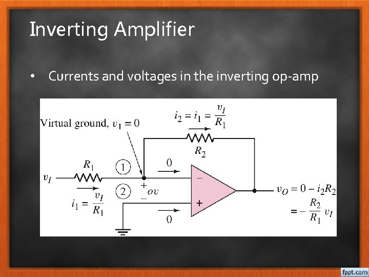
Inverting Amplifier • Currents and voltages in the inverting op-amp

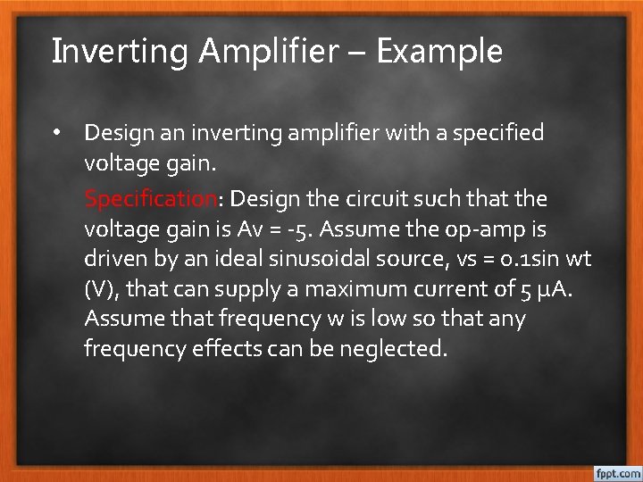
Inverting Amplifier – Example • Design an inverting amplifier with a specified voltage gain. Specification: Design the circuit such that the voltage gain is Av = -5. Assume the op-amp is driven by an ideal sinusoidal source, vs = 0. 1 sin wt (V), that can supply a maximum current of 5 µA. Assume that frequency w is low so that any frequency effects can be neglected.

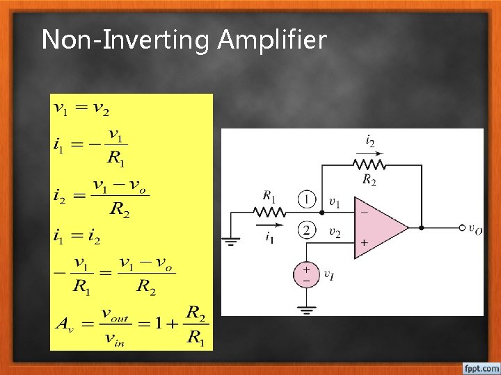
Non-Inverting Amplifier

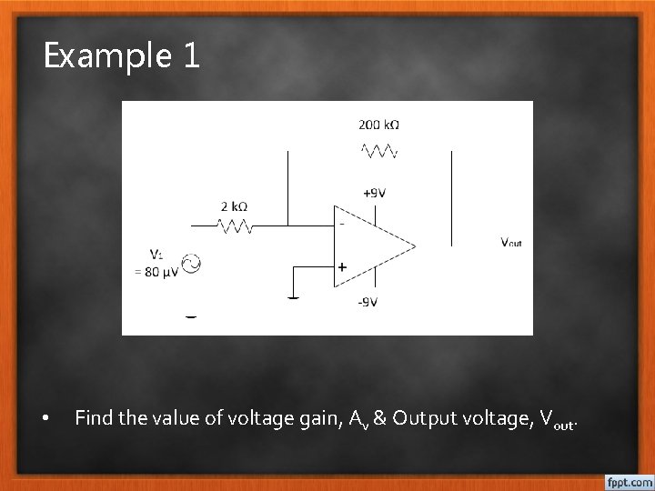
Example 1 • Find the value of voltage gain, Av & Output voltage, Vout.

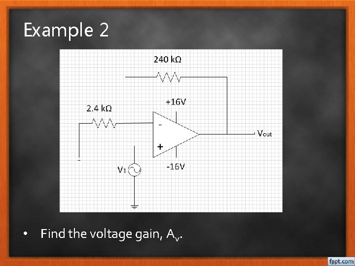
Example 2 • Find the voltage gain, Av.

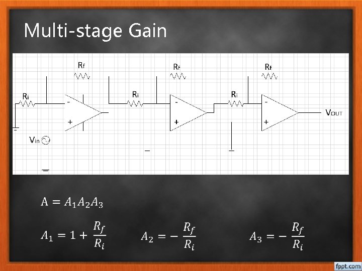
Multi-stage Gain

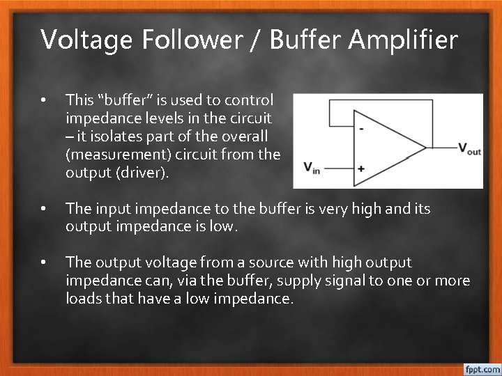
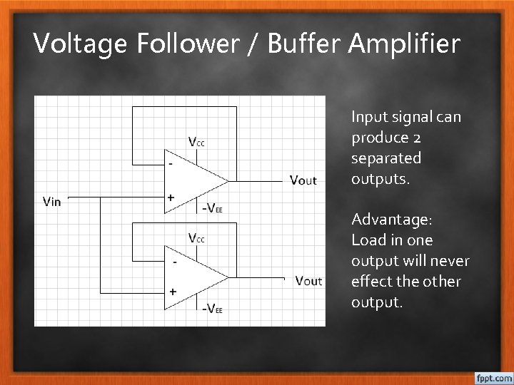
Voltage Follower / Buffer Amplifier • This “buffer” is used to control impedance levels in the circuit – it isolates part of the overall (measurement) circuit from the output (driver). • The input impedance to the buffer is very high and its output impedance is low. • The output voltage from a source with high output impedance can, via the buffer, supply signal to one or more loads that have a low impedance.

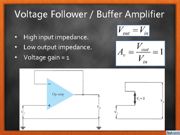
Voltage Follower / Buffer Amplifier • High input impedance. • Low output impedance. • Voltage gain = 1

Voltage Follower / Buffer Amplifier Input signal can produce 2 separated outputs. Advantage: Load in one output will never effect the other output.

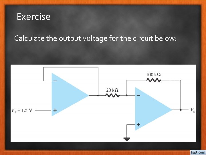
Exercise Calculate the output voltage for the circuit below:

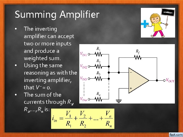
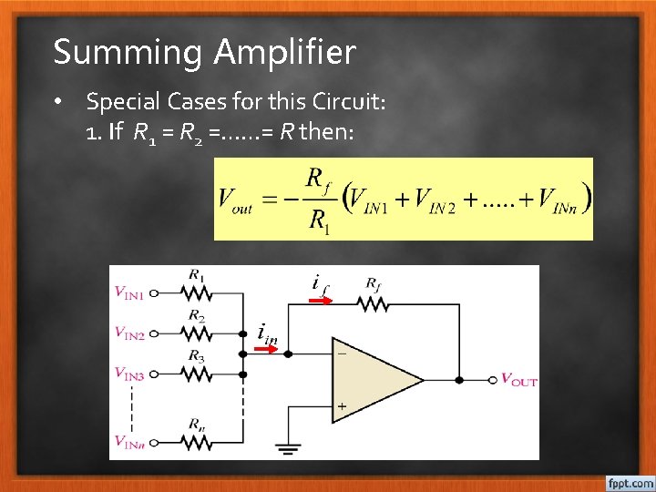
Summing Amplifier • • • The inverting amplifier can accept two or more inputs and produce a weighted sum. Using the same reasoning as with the inverting amplifier, that V ≈ 0. The sum of the currents through R 1, R 2, …, Rn is:

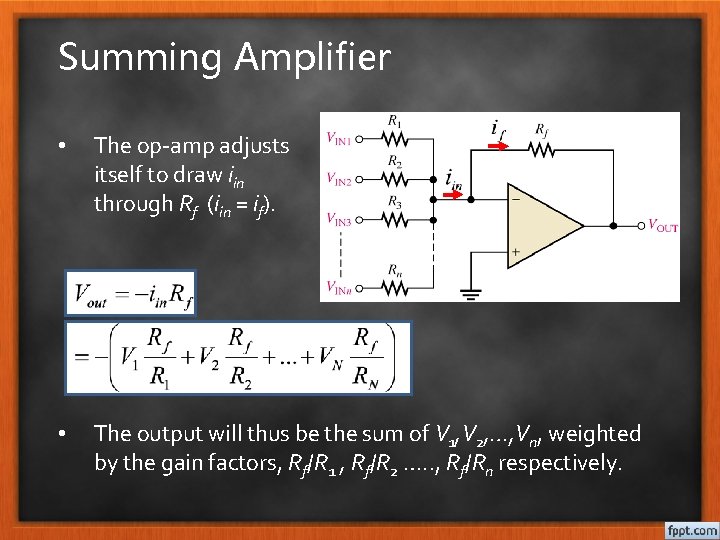
Summing Amplifier • The op-amp adjusts itself to draw iin through Rf (iin = if). • The output will thus be the sum of V 1, V 2, …, Vn, weighted by the gain factors, Rf/R 1 , Rf/R 2 …. . , Rf/Rn respectively.

Summing Amplifier • Special Cases for this Circuit: 1. If R 1 = R 2 =……= R then:

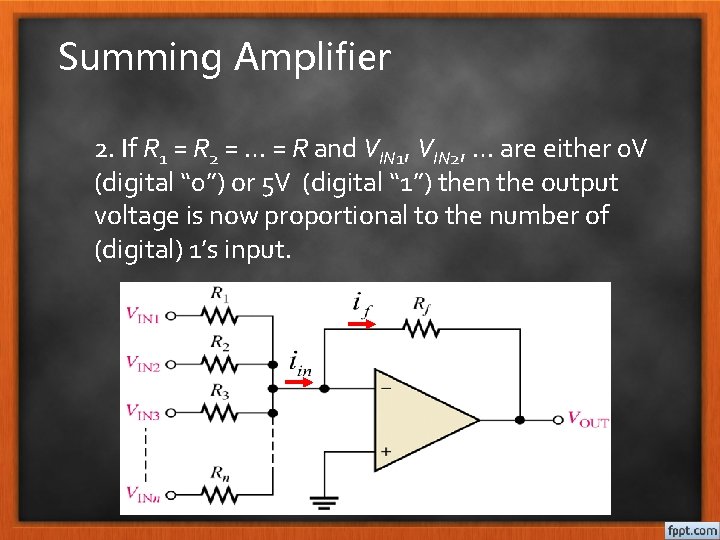
Summing Amplifier 2. If R 1 = R 2 = … = R and VIN 1, VIN 2, … are either 0 V (digital “ 0”) or 5 V (digital “ 1”) then the output voltage is now proportional to the number of (digital) 1’s input.

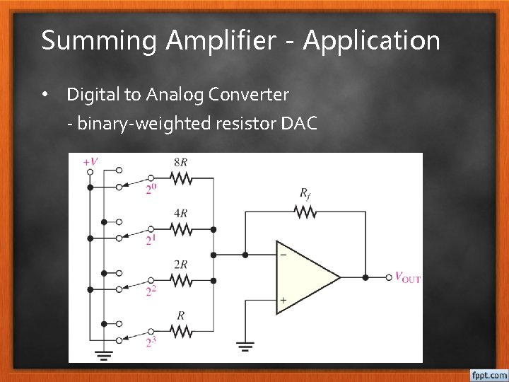
Summing Amplifier - Application • Digital to Analog Converter - binary-weighted resistor DAC

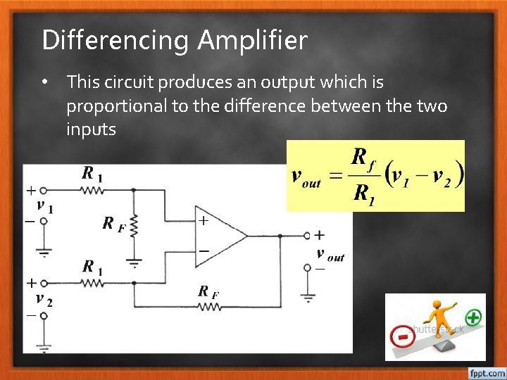
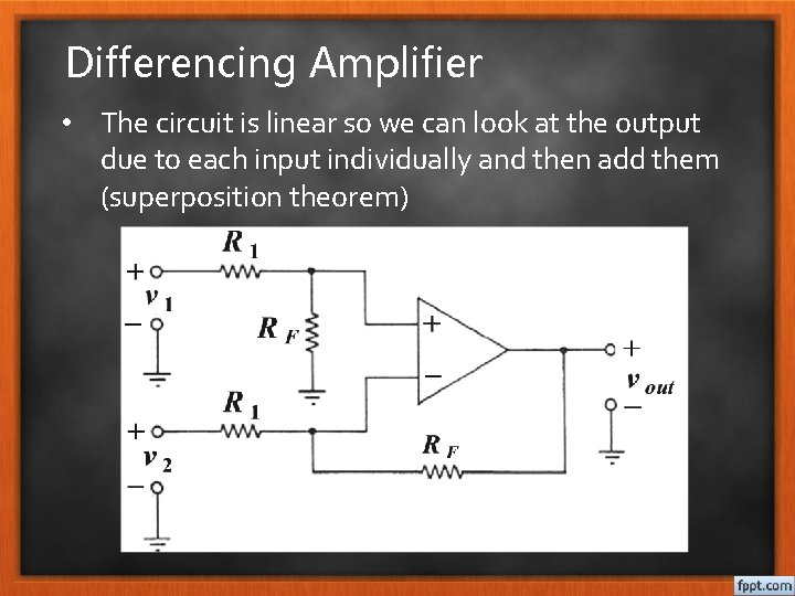
Differencing Amplifier • This circuit produces an output which is proportional to the difference between the two inputs

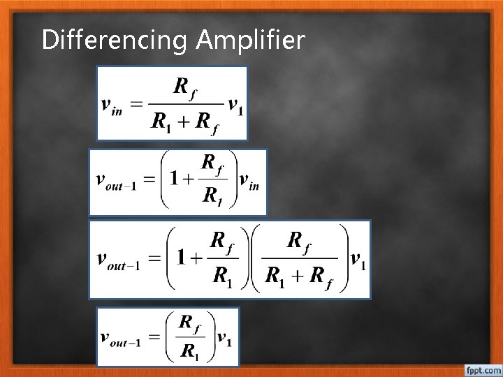
Differencing Amplifier • The circuit is linear so we can look at the output due to each input individually and then add them (superposition theorem)

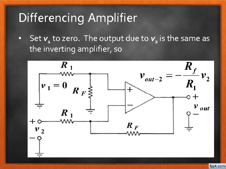
Differencing Amplifier • Set v 1 to zero. The output due to v 2 is the same as the inverting amplifier, so

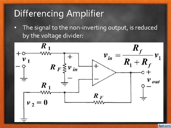
Differencing Amplifier • The signal to the non-inverting output, is reduced by the voltage divider:

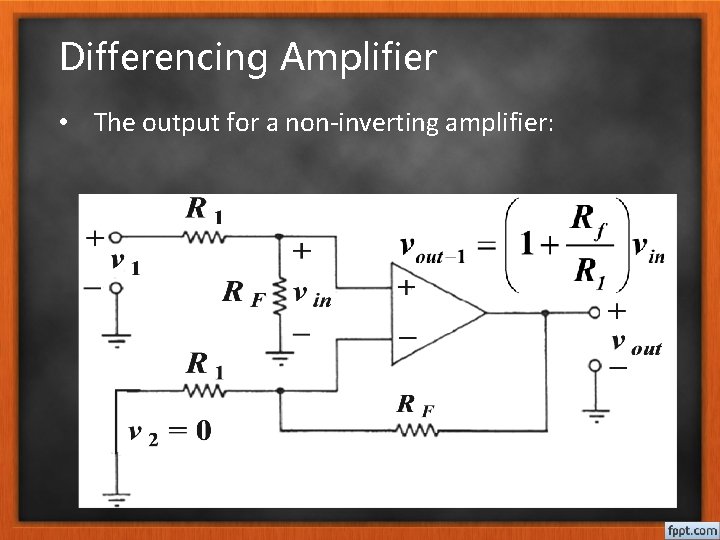
Differencing Amplifier • The output for a non-inverting amplifier:

Differencing Amplifier

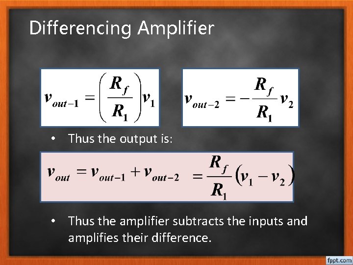
Differencing Amplifier • Thus the output is: • Thus the amplifier subtracts the inputs and amplifies their difference.

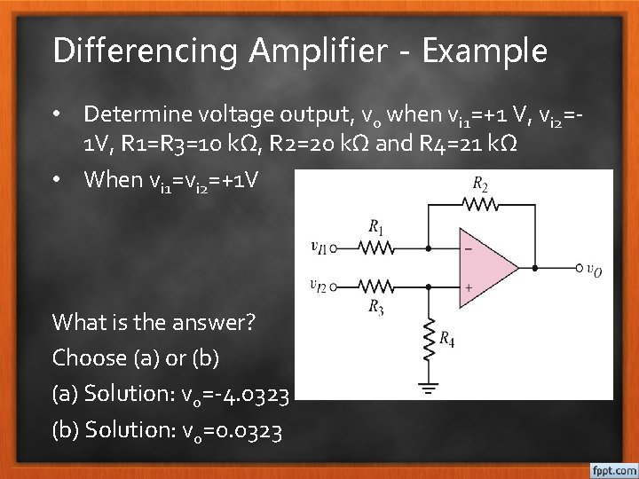
Differencing Amplifier - Example • Determine voltage output, vo when vi 1=+1 V, vi 2=1 V, R 1=R 3=10 kΩ, R 2=20 kΩ and R 4=21 kΩ • When vi 1=vi 2=+1 V What is the answer? Choose (a) or (b) (a) Solution: vo=-4. 0323 (b) Solution: vo=0. 0323

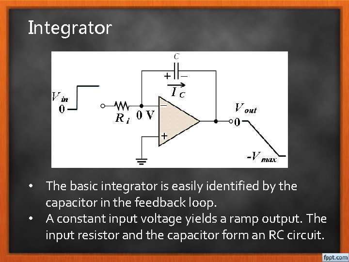
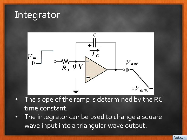
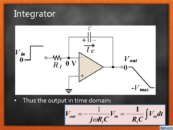
Integrator • The basic integrator is easily identified by the capacitor in the feedback loop. • A constant input voltage yields a ramp output. The input resistor and the capacitor form an RC circuit.

Integrator • The slope of the ramp is determined by the RC time constant. • The integrator can be used to change a square wave input into a triangular wave output.

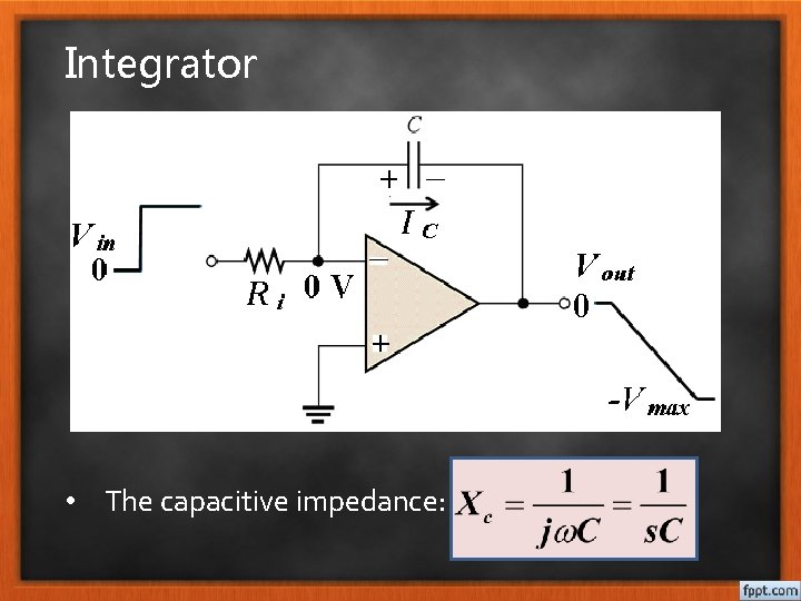
Integrator • The capacitive impedance:

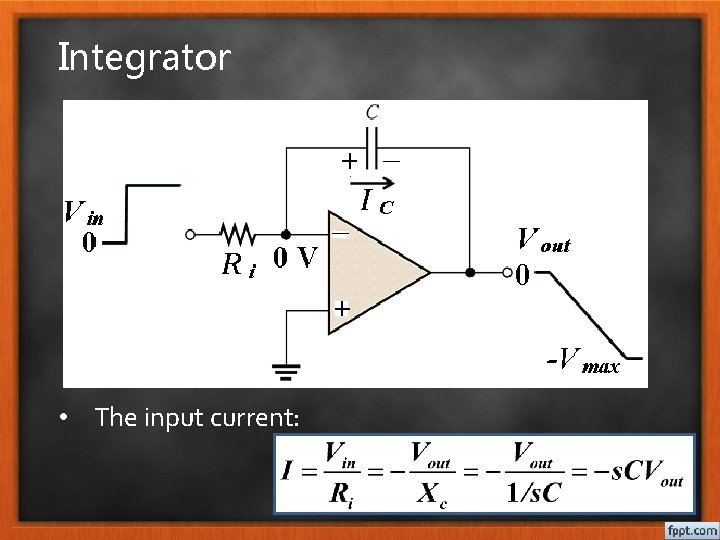
Integrator • The input current:

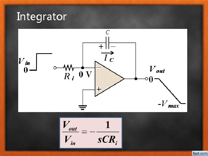
Integrator

Integrator • Thus the output in time domain:

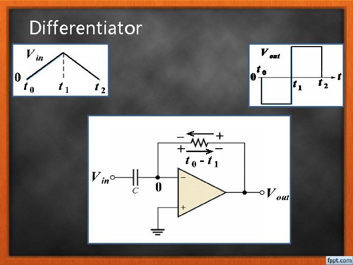
Differentiator

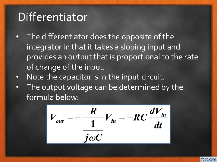
Differentiator • The differentiator does the opposite of the integrator in that it takes a sloping input and provides an output that is proportional to the rate of change of the input. • Note the capacitor is in the input circuit. • The output voltage can be determined by the formula below:

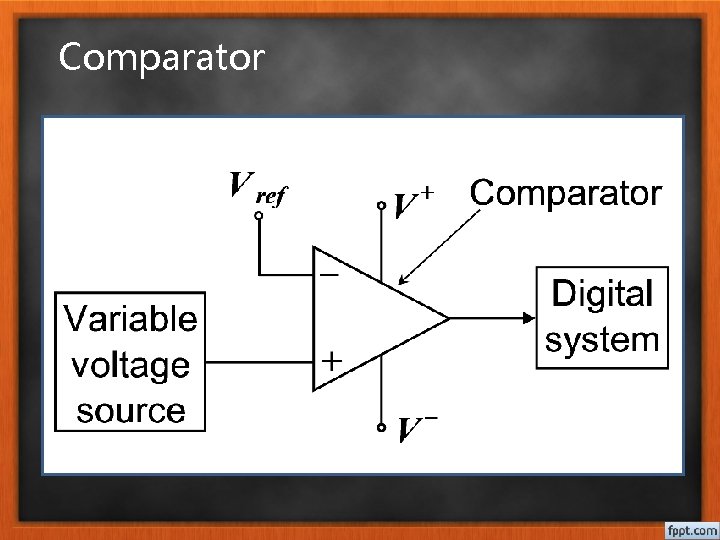
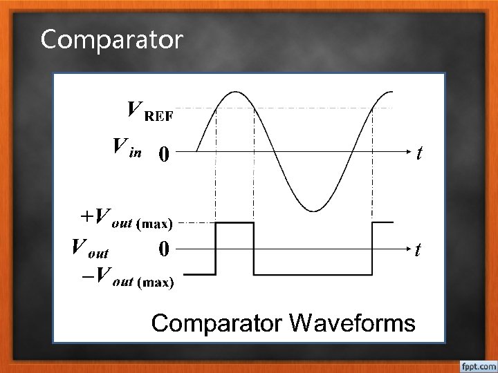
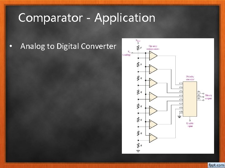
Comparator • The comparator is an op-amp circuit that compares two input voltages and produces an output indicating the relationship between them. • The inputs can be two signals (such as two sine waves) or a signal and a fixed dc reference voltage. • Comparators are most commonly used in digital applications.

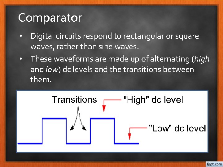
Comparator • Digital circuits respond to rectangular or square waves, rather than sine waves. • These waveforms are made up of alternating (high and low) dc levels and the transitions between them.

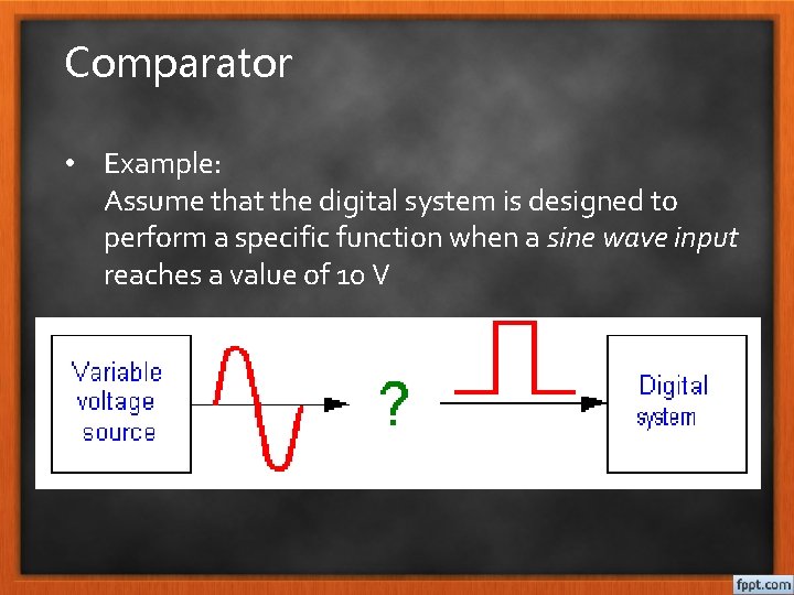
Comparator • Example: Assume that the digital system is designed to perform a specific function when a sine wave input reaches a value of 10 V

Comparator

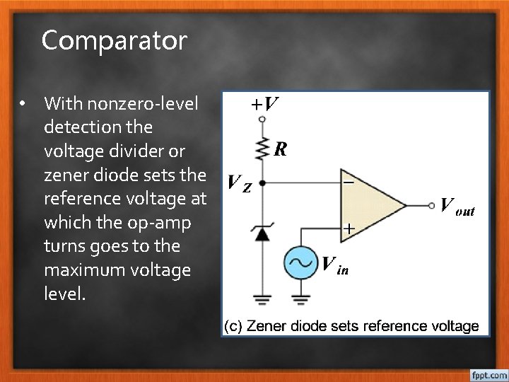
Comparator • With nonzero-level detection the voltage divider or zener diode sets the reference voltage at which the op-amp turns goes to the maximum voltage level.

Comparator

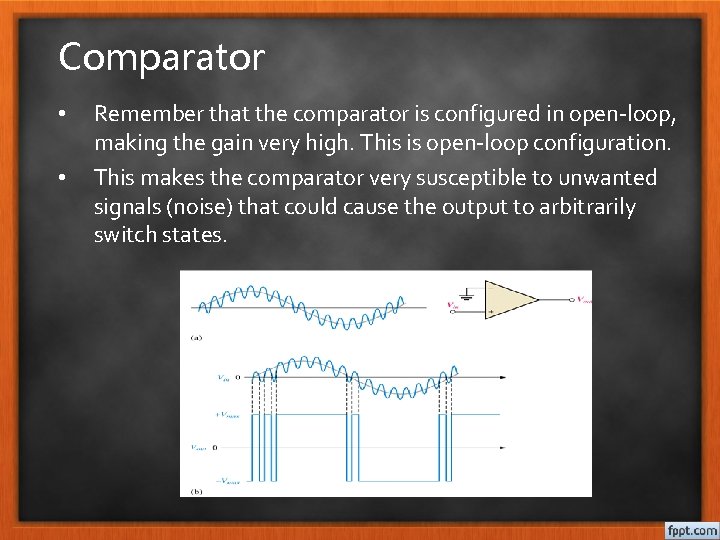
Comparator • • Remember that the comparator is configured in open-loop, making the gain very high. This is open-loop configuration. This makes the comparator very susceptible to unwanted signals (noise) that could cause the output to arbitrarily switch states.

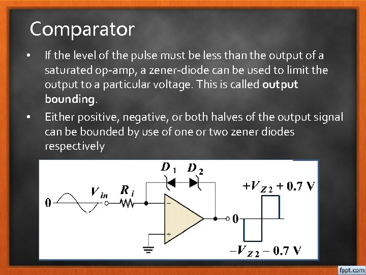
Comparator • • If the level of the pulse must be less than the output of a saturated op-amp, a zener-diode can be used to limit the output to a particular voltage. This is called output bounding. Either positive, negative, or both halves of the output signal can be bounded by use of one or two zener diodes respectively

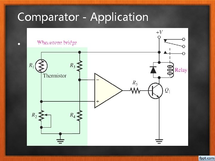
Comparator - Application • Over-Temperature Sensing circuit

Comparator - Application • Analog to Digital Converter

Summary • • • The summing amplifier’s output is the sum of the inputs. An averaging amplifier yields an output that is the average of all the inputs. The scaling adder has inputs of different weight with each contributing more or less to the input. Integrators change a constant voltage input to a sloped output. Differentiators change a sloping input into a step voltage proportional to the rate of change. The op-amp comparator’s output changes state when the input voltage exceeds the reference voltage.

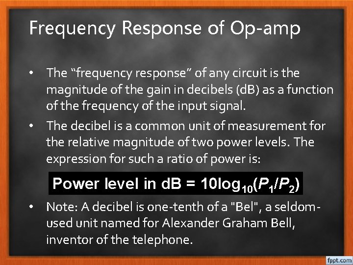
Frequency Response of Op-amp • The “frequency response” of any circuit is the magnitude of the gain in decibels (d. B) as a function of the frequency of the input signal. • The decibel is a common unit of measurement for the relative magnitude of two power levels. The expression for such a ratio of power is: Power level in d. B = 10 log 10(P 1/P 2) • Note: A decibel is one-tenth of a "Bel", a seldomused unit named for Alexander Graham Bell, inventor of the telephone.

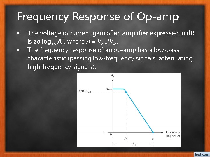
Frequency Response of Op-amp • • The voltage or current gain of an amplifier expressed in d. B is 20 log 10|A|, where A = Vout/Vin. The frequency response of an op-amp has a low-pass characteristic (passing low-frequency signals, attenuating high-frequency signals).

Frequency Response of Op-amp • The bandwidth is the frequency at which the power of the output signal is reduced to half that of the maximum output power. • This occurs when the power gain A drops by 3 d. B. In Figure shown before, the bandwidth is fc Hz. • For all op-amps, the Gain*Bandwidth product is a constant. • Hence, if the gain of an op-amp is decreased, its operational bandwidth increases proportionally.

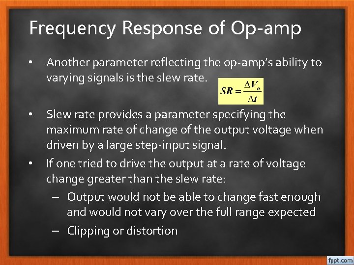
Frequency Response of Op-amp • Another parameter reflecting the op-amp’s ability to varying signals is the slew rate. • Slew rate provides a parameter specifying the maximum rate of change of the output voltage when driven by a large step-input signal. If one tried to drive the output at a rate of voltage change greater than the slew rate: – Output would not be able to change fast enough and would not vary over the full range expected – Clipping or distortion •

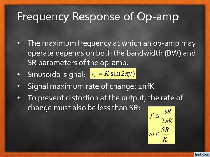
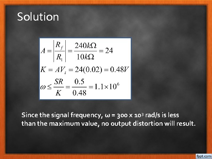
Frequency Response of Op-amp • The maximum frequency at which an op-amp may operate depends on both the bandwidth (BW) and SR parameters of the op-amp. • Sinusoidal signal: • Signal maximum rate of change: 2πf. K • To prevent distortion at the output, the rate of change must also be less than SR:

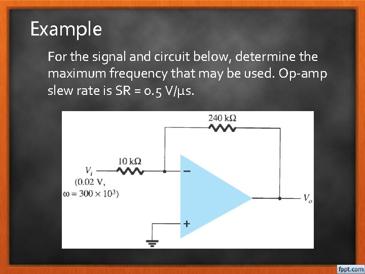
Example For the signal and circuit below, determine the maximum frequency that may be used. Op-amp slew rate is SR = 0. 5 V/µs.

Solution Since the signal frequency, ω = 300 x 103 rad/s is less than the maximum value, no output distortion will result.