Digital Systems Lecture 8 Dr Ing Erwin Sitompul
- Slides: 34

Digital Systems Lecture 8 Dr. -Ing. Erwin Sitompul President University http: //zitompul. wordpress. com 2 0 1 7 President University Erwin Sitompul Digital Systems 8/1

Digital Systems Section 10 Sequential Circuits: Flip-Flops President University Erwin Sitompul Digital Systems 8/2

Lecture Digital Systems Clock Signals n Digital systems can operate either asynchronously or synchronously. n In asynchronous systems, the outputs of logic circuits can change state any time one or more of the inputs change. n In synchronous system, the exact times at which any output can change states are determined by a signal commonly called as the enable/control or the clock. n Enable/control is used in latch circuit. The inputs can affect the output only when the enable/control signal has a certain value. n Clock is used in flip-flop circuit. The inputs can affect the output only when the clock signal changes (rising/positive edge or falling/negative edge). President University Erwin Sitompul Digital Systems 8/3

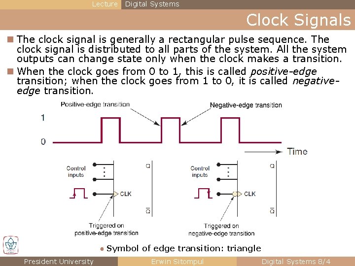
Lecture Digital Systems Clock Signals n The clock signal is generally a rectangular pulse sequence. The clock signal is distributed to all parts of the system. All the system outputs can change state only when the clock makes a transition. n When the clock goes from 0 to 1, this is called positive-edge transition; when the clock goes from 1 to 0, it is called negativeedge transition. ● Symbol of edge transition: triangle President University Erwin Sitompul Digital Systems 8/4

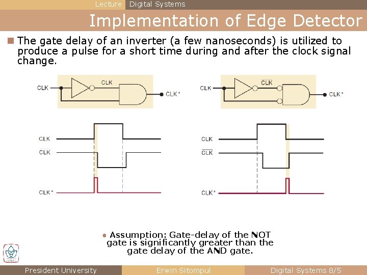
Lecture Digital Systems Implementation of Edge Detector n The gate delay of an inverter (a few nanoseconds) is utilized to produce a pulse for a short time during and after the clock signal change. ● Assumption: Gate-delay of the NOT gate is significantly greater than the gate delay of the AND gate. President University Erwin Sitompul Digital Systems 8/5

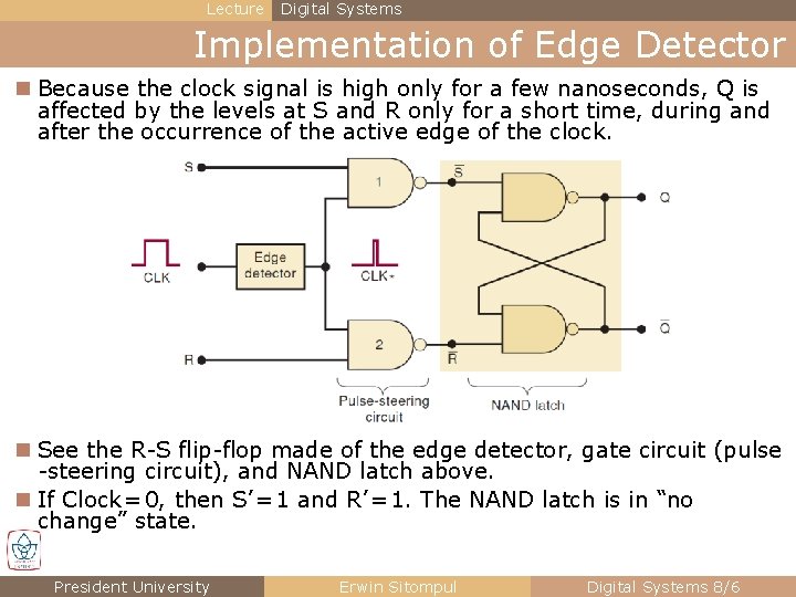
Lecture Digital Systems Implementation of Edge Detector n Because the clock signal is high only for a few nanoseconds, Q is affected by the levels at S and R only for a short time, during and after the occurrence of the active edge of the clock. n See the R-S flip-flop made of the edge detector, gate circuit (pulse -steering circuit), and NAND latch above. n If Clock = 0, then S’ = 1 and R’ = 1. The NAND latch is in “no change” state. President University Erwin Sitompul Digital Systems 8/6

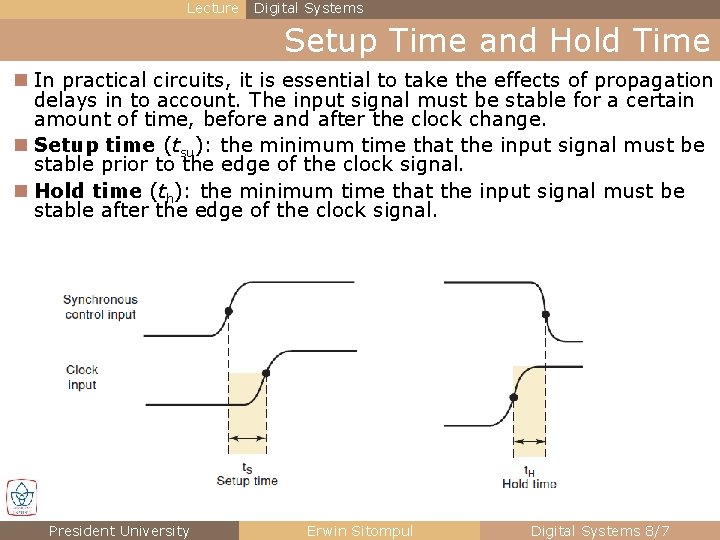
Lecture Digital Systems Setup Time and Hold Time n In practical circuits, it is essential to take the effects of propagation delays in to account. The input signal must be stable for a certain amount of time, before and after the clock change. n Setup time (tsu): the minimum time that the input signal must be stable prior to the edge of the clock signal. n Hold time (th): the minimum time that the input signal must be stable after the edge of the clock signal. President University Erwin Sitompul Digital Systems 8/7

Lecture Digital Systems Flip-Flops n A flip-flop is a storage element based on the gated latch principle. n The output of a flip-flop output depends on the clock signal. n Flip-flops are edge-triggered: output changes happen only when the active edge of the clock occurs. The active edge can be positive-edge (clock change from low to high) or negative-edge (clock change from high to low). n Flip-flops can be built from one gated latch or two latches (i. e. , master-slave flip-flop). n Master-slave flip-flops: consist of 2 latches, output changes in every full cycle of the clock. In one half-cycle, the master is active and the input is acquired, in the other half-cycle, the slave is active and the input is delivered to the output. President University Erwin Sitompul Digital Systems 8/8

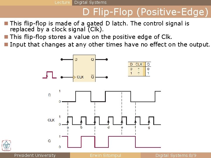
Lecture Digital Systems D Flip-Flop (Positive-Edge) n This flip-flop is made of a gated D latch. The control signal is replaced by a clock signal (Clk). n This flip-flop stores a value on the positive edge of Clk. n Input that changes at any other times have no effect on the output. President University Erwin Sitompul Digital Systems 8/9

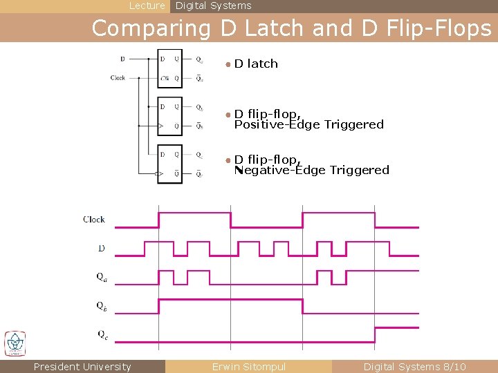
Lecture Digital Systems Comparing D Latch and D Flip-Flops ● D latch ● D flip-flop, Positive-Edge Triggered ● D flip-flop, Negative-Edge Triggered President University Erwin Sitompul Digital Systems 8/10

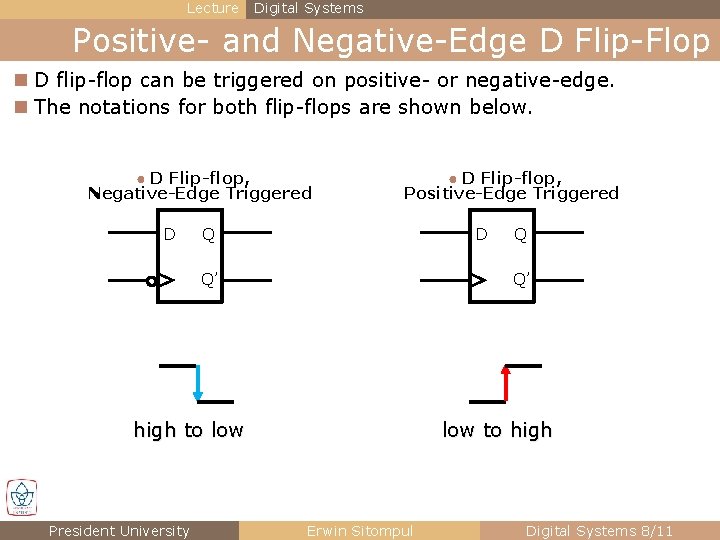
Lecture Digital Systems Positive- and Negative-Edge D Flip-Flop n D flip-flop can be triggered on positive- or negative-edge. n The notations for both flip-flops are shown below. ● D Flip-flop, Negative-Edge Triggered D ● D Flip-flop, Positive-Edge Triggered D Q Q’ Q’ low to high to low President University Q Erwin Sitompul Digital Systems 8/11

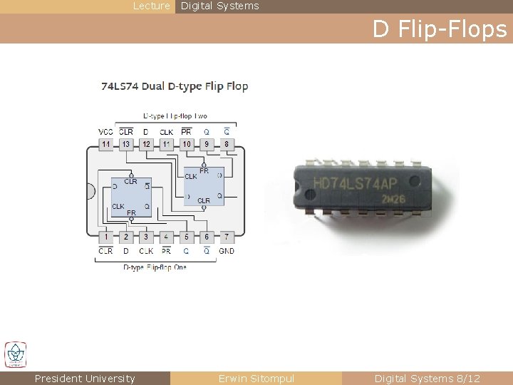
Lecture Digital Systems D Flip-Flops President University Erwin Sitompul Digital Systems 8/12

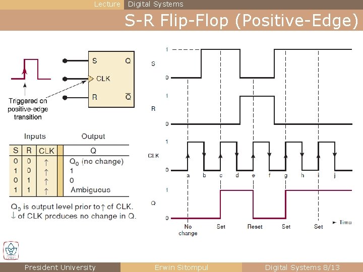
Lecture Digital Systems S-R Flip-Flop (Positive-Edge) President University Erwin Sitompul Digital Systems 8/13

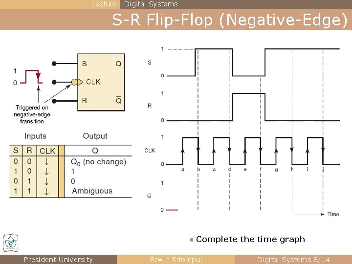
Lecture Digital Systems S-R Flip-Flop (Negative-Edge) ● Complete the time graph President University Erwin Sitompul Digital Systems 8/14

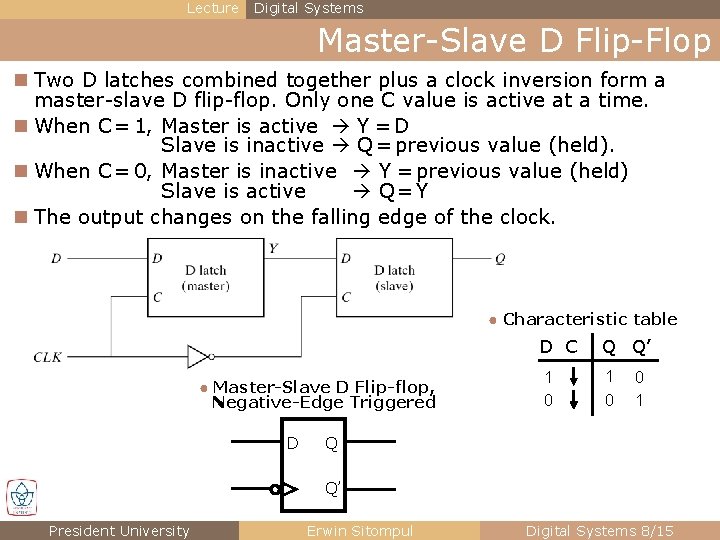
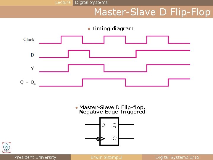
Lecture Digital Systems Master-Slave D Flip-Flop n Two D latches combined together plus a clock inversion form a master-slave D flip-flop. Only one C value is active at a time. n When C = 1, Master is active Y = D Slave is inactive Q = previous value (held). n When C = 0, Master is inactive Y = previous value (held) Slave is active Q=Y n The output changes on the falling edge of the clock. ● Characteristic table D C ● Master-Slave D Flip-flop, Negative-Edge Triggered D 1 0 Q Q’ /1 0 0 1 Q Q’ President University Erwin Sitompul Digital Systems 8/15

Lecture Digital Systems Master-Slave D Flip-Flop ● Timing diagram ● Master-Slave D Flip-flop, Negative-Edge Triggered D Q Q’ President University Erwin Sitompul Digital Systems 8/16

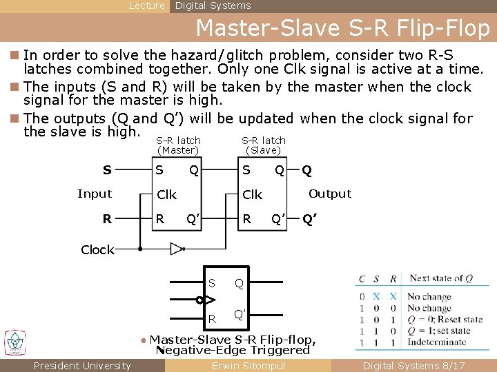
Lecture Digital Systems Master-Slave S-R Flip-Flop n In order to solve the hazard/ glitch problem, consider two R-S latches combined together. Only one Clk signal is active at a time. n The inputs (S and R) will be taken by the master when the clock signal for the master is high. n The outputs (Q and Q’) will be updated when the clock signal for the slave is high. S Input R S-R latch (Master) S-R latch (Slave) S S Q Clk R Q Output Clk Q’ R Q Q’ Q’ Clock S Q R Q’ ● Master-Slave S-R Flip-flop, Negative-Edge Triggered President University Erwin Sitompul Digital Systems 8/17

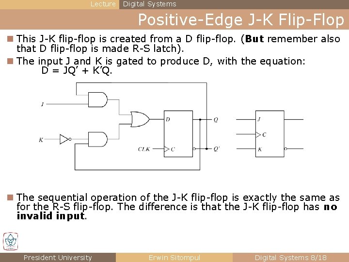
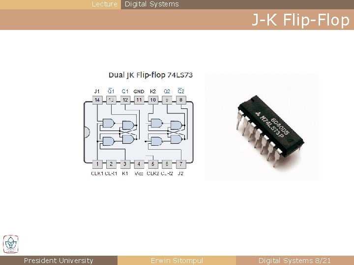
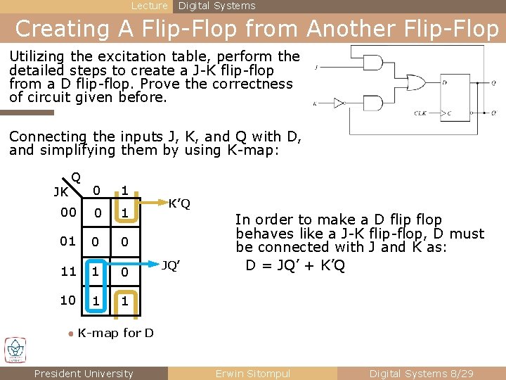
Lecture Digital Systems Positive-Edge J-K Flip-Flop n This J-K flip-flop is created from a D flip-flop. (But remember also that D flip-flop is made R-S latch). n The input J and K is gated to produce D, with the equation: D = JQ’ + K’Q. n The sequential operation of the J-K flip-flop is exactly the same as for the R-S flip-flop. The difference is that the J-K flip-flop has no invalid input. President University Erwin Sitompul Digital Systems 8/18

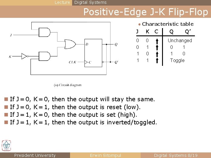
Lecture Digital Systems Positive-Edge J-K Flip-Flop ● Characteristic table n If J = 0, J = 1, K = 0, K = 1, then President University the the output J K C 0 0 1 1 0 1 Q Q’ Unchanged 0 1 Toggle will stay the same. is reset (low). is set (high). is inverted/toggled. Erwin Sitompul Digital Systems 8/19

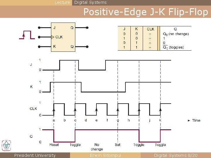
Lecture Digital Systems Positive-Edge J-K Flip-Flop Two data inputs, J and K J -> set, K -> reset, if J=K=1 then toggle output President University Erwin Sitompul Digital Systems 8/20

Lecture Digital Systems J-K Flip-Flop President University Erwin Sitompul Digital Systems 8/21

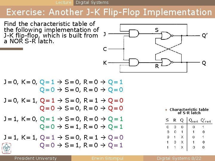
Lecture Digital Systems Exercise: Another J-K Flip-Flop Implementation Find the characteristic table of the following implementation of J-K flip-flop, which is built from J a NOR S-R latch. S Q’ C K Q R J = 0, K = 0, Q = 1 S = 0, R = 0 Q = 1 Q = 0 S = 0, R = 0 Q = 0 J = 0, K = 1, Q = 1 S = 0, R = 1 Q = 0 S = 0, R = 0 Q = 0 ● Characteristic table of S-R latch J = 1, K = 0, Q = 1 S = 0, R = 0 Q = 1 Q = 0 S = 1, R = 0 Q = 1 J = 1, K = 1, Q = 1 S = 0, R = 1 Q = 0 S = 1, R = 0 Q = 1 President University Erwin Sitompul Digital Systems 8/22

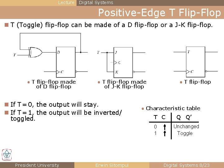
Lecture Digital Systems Positive-Edge T Flip-Flop n T (Toggle) flip-flop can be made of a D flip-flop or a J-K flip-flop. ● T flip-flop made of D flip-flop ● T flip-flop made of J-K flip-flop n If T = 0, the output will stay. n If T = 1, the output will be inverted/ toggled. ● T flip-flop ● Characteristic table T C 0 1 President University Erwin Sitompul Q Q’ Unchanged Toggle Digital Systems 8/23

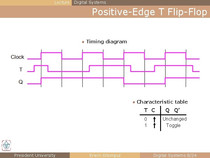
Lecture Digital Systems Positive-Edge T Flip-Flop ● Timing diagram ● Characteristic table T C 0 1 President University Erwin Sitompul Q Q’ Unchanged Toggle Digital Systems 8/24

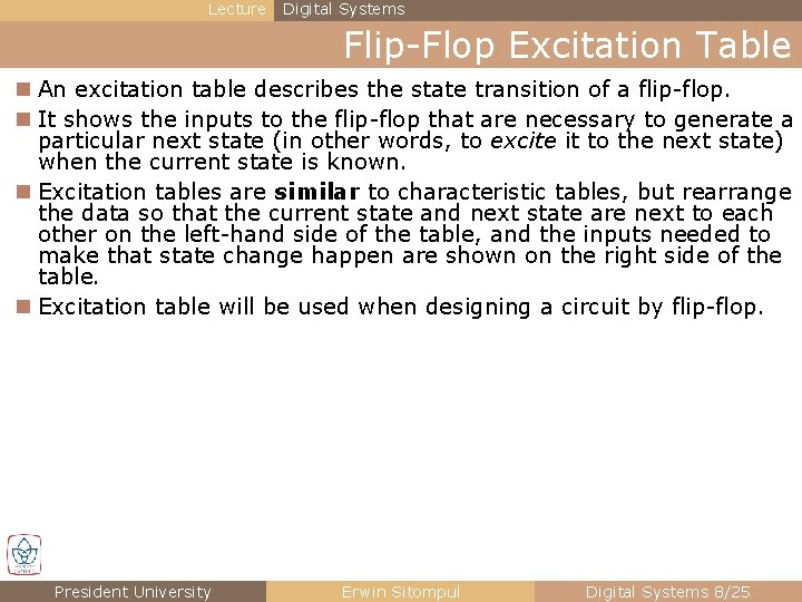
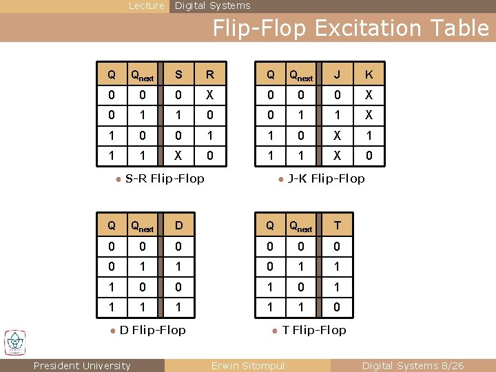
Lecture Digital Systems Flip-Flop Excitation Table n An excitation table describes the state transition of a flip-flop. n It shows the inputs to the flip-flop that are necessary to generate a particular next state (in other words, to excite it to the next state) when the current state is known. n Excitation tables are similar to characteristic tables, but rearrange the data so that the current state and next state are next to each other on the left-hand side of the table, and the inputs needed to make that state change happen are shown on the right side of the table. n Excitation table will be used when designing a circuit by flip-flop. President University Erwin Sitompul Digital Systems 8/25

Lecture Digital Systems Flip-Flop Excitation Table Q Qnext S R Q Qnext J K 0 0 0 X 0 1 1 0 0 1 1 X 1 0 0 1 1 0 X 1 1 1 X 0 ● S-R Flip-Flop ● J-K Flip-Flop Q Qnext D Q Qnext T 0 0 0 0 1 1 1 1 0 ● D Flip-Flop President University ● T Flip-Flop Erwin Sitompul Digital Systems 8/26

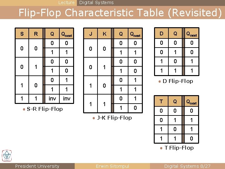
Lecture Digital Systems Flip-Flop Characteristic Table (Revisited) S 0 0 R 0 1 1 Q Qnext 0 0 1 1 1 inv ● S-R Flip-Flop J 0 0 1 1 K 0 1 Q Qnext D Q Qnext 0 0 0 1 1 0 1 1 1 0 ● J-K Flip-Flop ● D Flip-Flop T Q Qnext 0 0 1 1 1 0 ● T Flip-Flop President University Erwin Sitompul Digital Systems 8/27

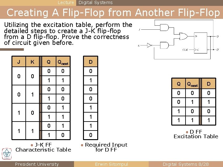
Lecture Digital Systems Creating A Flip-Flop from Another Flip-Flop Utilizing the excitation table, perform the detailed steps to create a J-K flip-flop from a D flip-flop. Prove the correctness of circuit given before. J 0 0 1 1 K 0 1 Q Qnext D 0 0 ? 0 1 1 ? 1 0 0 0 1 1 1 0 0 ● J-K FF Characteristic Table President University Q Qnext D 0 0 1 1 1 ● D FF Excitation Table ● Required Input for D FF Erwin Sitompul Digital Systems 8/28

Lecture Digital Systems Creating A Flip-Flop from Another Flip-Flop Utilizing the excitation table, perform the detailed steps to create a J-K flip-flop from a D flip-flop. Prove the correctness of circuit given before. Connecting the inputs J, K, and Q with D, and simplifying them by using K-map: Q 0 1 00 0 1 01 0 0 11 1 0 10 1 1 JK K’Q JQ’ In order to make a D flip flop behaves like a J-K flip-flop, D must be connected with J and K as: D = JQ’ + K’Q ● K-map for D President University Erwin Sitompul Digital Systems 8/29

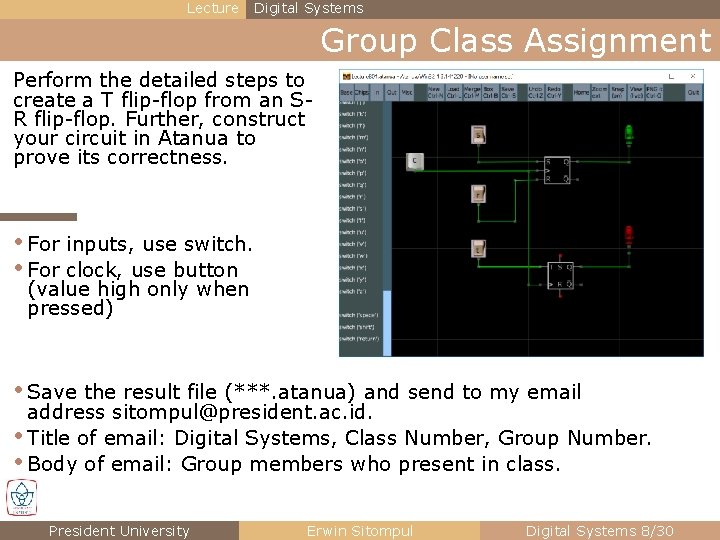
Lecture Digital Systems Group Class Assignment Perform the detailed steps to create a T flip-flop from an SR flip-flop. Further, construct your circuit in Atanua to prove its correctness. • For inputs, use switch. • For clock, use button (value high only when pressed) • Save the result file (***. atanua) and send to my email address sitompul@president. ac. id. • Title of email: Digital Systems, Class Number, Group Number. • Body of email: Group members who present in class. President University Erwin Sitompul Digital Systems 8/30

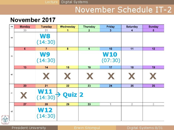
Lecture Digital Systems November Schedule IT-2 W 8 (14: 30) W 9 W 10 (14: 30) X X W 11 (07: 30) X X X Quiz 2 (14: 30) W 12 (14: 30) President University Erwin Sitompul Digital Systems 8/31

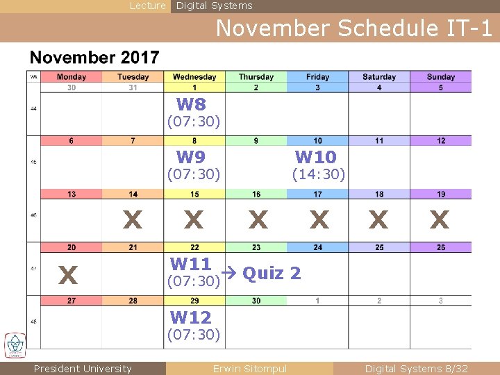
Lecture Digital Systems November Schedule IT-1 W 8 (07: 30) W 9 W 10 (07: 30) X X X W 11 (14: 30) X X Quiz 2 (07: 30) W 12 (07: 30) President University Erwin Sitompul Digital Systems 8/32

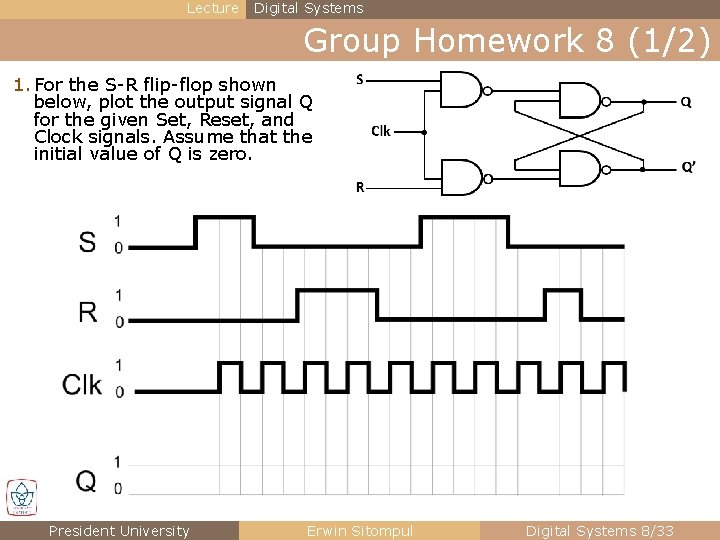
Lecture Digital Systems Group Homework 8 (1/2) 1. For the S-R flip-flop shown below, plot the output signal Q for the given Set, Reset, and Clock signals. Assume that the initial value of Q is zero. President University Erwin Sitompul Digital Systems 8/33

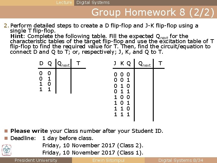
Lecture Digital Systems Group Homework 8 (2/2) 2. Perform detailed steps to create a D flip-flop and J-K flip-flop using a single T flip-flop. Hint: Complete the following table. Fill the expected Qnext for the characteristic tables of the target flip-flop and use the excitation table of T flip-flop to find the required value for T. Then, find the circuit/equation to connect D and Q to T; or, respectively; J, K, and Q to T. D Q Qnext 0 0 1 1 0 1 T J K Q 0 0 1 1 Qnext T 0 1 0 1 n Please write your Class number after your Student ID. n Deadline: 1 day before class. Friday, 10 November 2017 (Class 2). Friday, 10 November 2017 (Class 1). President University Erwin Sitompul Digital Systems 8/34