Data transmitting ASIC for liquid Argon TPC for
- Slides: 33

Data transmitting ASIC for liquid Argon TPC for the DUNE experiment Davide Braga, Fermilab Front End Electronics, Jouvence, 21 May 2018

Outline • • Cold electronics for DUNE Requirements for cryogenic operation, HCE and choice of technology Development of custom cryogenic Spice models Development of a custom library of standard cells for cryogenic operation LVDS Transmitter and Receiver COLDATA CDP 1: COLDATA Prototype chip • Test setup and results • Conclusions 2 5/21/2018 Davide Braga | FEE 2018

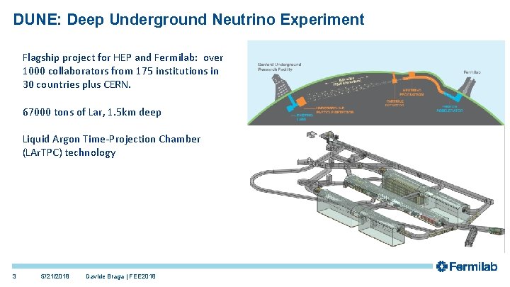
DUNE: Deep Underground Neutrino Experiment Flagship project for HEP and Fermilab: over 1000 collaborators from 175 institutions in 30 countries plus CERN. 67000 tons of Lar, 1. 5 km deep Liquid Argon Time-Projection Chamber (LAr. TPC) technology 3 5/21/2018 Davide Braga | FEE 2018

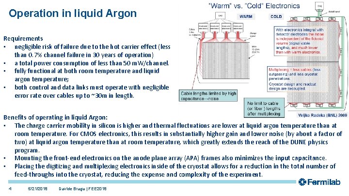
Operation in liquid Argon Requirements • negligible risk of failure due to the hot carrier effect (less than 0. 7% channel failure in 30 years of operation) • a total power consumption of less than 50 m. W/channel. • fully functional at both room temperature and liquid argon temperature; • both control and data links must operate with negligible error rate over cables up to ~30 m in length. Benefits of operating in liquid Argon: • The charge carrier mobility in silicon is higher and thermal fluctuations are lower at liquid argon temperature than at room temperature. For CMOS electronics, this results in substantially higher gain and lower noise (by about a factor of two) at liquid argon temperature than at room temperature, which greatly extends the reach of the DUNE physics program. • Mounting the front-end electronics on the anode plane array (APA) frames also minimizes the input capacitance. • Placing the digitizing and multiplexing electronics inside of the cryostat allows for a reduction in the total number of feed-throughs into the cryostat, reducing the expense and complexity of the experiment. 4 5/21/2018 Davide Braga | FEE 2018

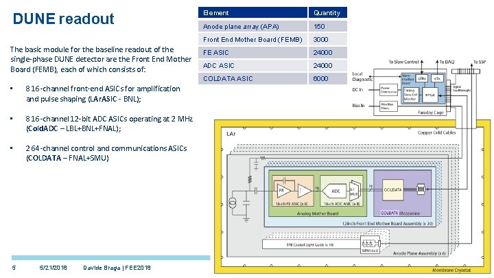
DUNE readout The basic module for the baseline readout of the single-phase DUNE detector are the Front End Mother Board (FEMB), each of which consists of: • 8 16 -channel front-end ASICs for amplification and pulse shaping (LAr. ASIC - BNL); • 8 16 -channel 12 -bit ADC ASICs operating at 2 MHz (Cold. ADC – LBL+BNL+FNAL); • 2 64 -channel control and communications ASICs (COLDATA – FNAL+SMU) 5 5/21/2018 Davide Braga | FEE 2018 Element Quantity Anode plane array (APA) 150 Front End Mother Board (FEMB) 3000 FE ASIC 24000 ADC ASIC 24000 COLDATA ASIC 6000

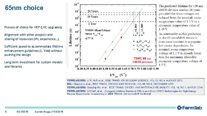
65 nm choice Process of choice for HEP (LHC upgrades). Alignment with other projects and sharing of resources (IPs, experience…). Sufficient speed to accommodate lifetime enhancement guidelines (L, Vdd) without pushing the design. Long term investment for custom models and libraries. 6 5/21/2018 Davide Braga | FEE 2018

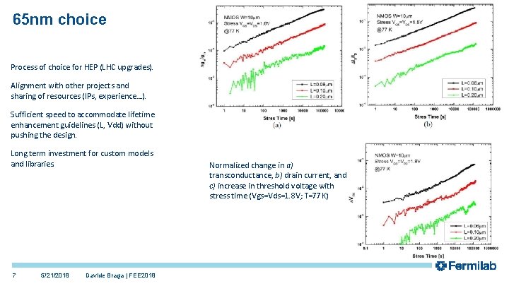
65 nm choice Process of choice for HEP (LHC upgrades). Alignment with other projects and sharing of resources (IPs, experience…). Sufficient speed to accommodate lifetime enhancement guidelines (L, Vdd) without pushing the design. Long term investment for custom models and libraries. 7 5/21/2018 Davide Braga | FEE 2018 Normalized change in a) transconductance, b) drain current, and c) increase in threshold voltage with stress time (Vgs=Vds=1. 8 V; T=77 K)

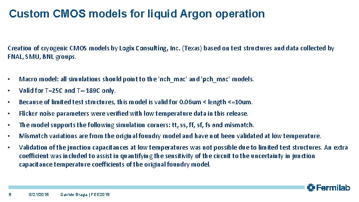
Custom CMOS models for liquid Argon operation Creation of cryogenic CMOS models by Logix Consulting, Inc. (Texas) based on test structures and data collected by FNAL, SMU, BNL groups. • Macro model: all simulations should point to the 'nch_mac' and 'pch_mac' models. • Valid for T=25 C and T=-189 C only. • Because of limited test structures, this model is valid for 0. 06 um < length <=10 um. • Flicker noise parameters were verified with low temperature data in this release. • The model supports the following simulation corners: tt, ss, ff, sf, fs and mismatch. • Mismatch variations are from the original foundry model and have not been validated at low temperature. • Validation of the junction capacitances at low temperatures was not possible due to limited test structures. An extra coefficient was included to assist in quantifying the sensitivity of the circuit to the uncertainty in junction capacitance temperature coefficients of the original foundry model. 8 5/21/2018 Davide Braga | FEE 2018

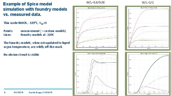
Example of Spice model simulation with foundry models vs. measured data. Thin oxide NMOS, -189°C, VBS=0 Points: Lines: measurement ( = custom models) foundry models at -189 C The foundry models, when extrapolated to liquid argon temperature, are wildly off-the-mark. No obvious trend is visible 9 5/21/2018 Davide Braga | FEE 2018

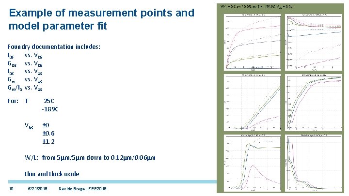
Example of measurement points and model parameter fit Foundry documentation includes: IDS vs. VDS GDS vs. VDS IDS vs. VGS Gm/ID vs. VGS For: T 25 C -189 C VBS ± 0. 6 ± 1. 2 W/L: from 5µm/5µm down to 0. 12µm/0. 06µm thin and thick oxide 10 5/21/2018 Davide Braga | FEE 2018

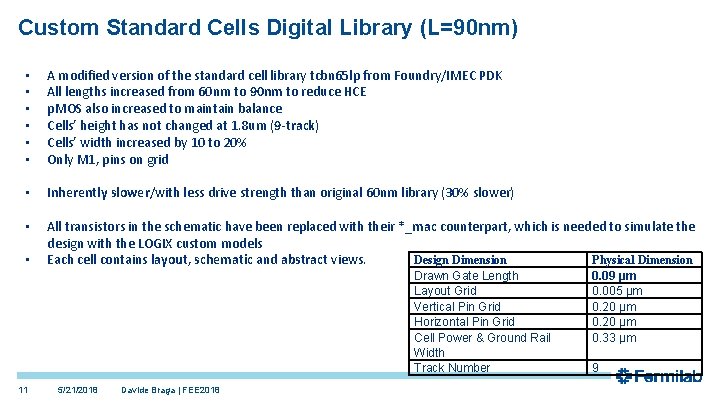
Custom Standard Cells Digital Library (L=90 nm) • • • A modified version of the standard cell library tcbn 65 lp from Foundry/IMEC PDK All lengths increased from 60 nm to 90 nm to reduce HCE p. MOS also increased to maintain balance Cells’ height has not changed at 1. 8 um (9 -track) Cells’ width increased by 10 to 20% Only M 1, pins on grid • Inherently slower/with less drive strength than original 60 nm library (30% slower) • All transistors in the schematic have been replaced with their *_mac counterpart, which is needed to simulate the design with the LOGIX custom models Design Dimension Physical Dimension Each cell contains layout, schematic and abstract views. • Drawn Gate Length Layout Grid Vertical Pin Grid Horizontal Pin Grid Cell Power & Ground Rail Width Track Number 11 5/21/2018 Davide Braga | FEE 2018 0. 09 μm 0. 005 μm 0. 20 μm 0. 33 μm 9

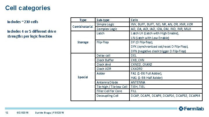
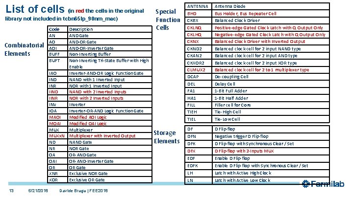
Cell categories Includes ~230 cells Includes 4 or 5 different drive strengths per logic function Type Sub-type Simple Logic Combinatorial Complex Logic Latch Storage Special Flip-Flop Delay cell Clock Buffer Clock And Clock XOR Adder Antenna Diode Tie-high / Tie-low Cell Filler Cell for Core Decoupling Cell 12 5/21/2018 Davide Braga | FEE 2018 Cells INV, BUFF, BUFT, ND, NR, AN, OR, XNR, XOR AO, OA, AOI, IAO, IOA, OAI, IND, INR, MUX Latch LH (Latch with High Enable), LN (Latch with Low Enable) DF (D Flip-flop), DFK (synchronized set/reset D Flip-Flop), DFN (negative clock trigger D Flip-Flop) DEL CKB, CKND 2, CKAN 2 CKXOR 2 FA 1 (1 -Bit Full Adder), HA 1 (1 -Bit Half Adder) ANTENNA TIEH, TIEL FILL DCAP, DCAP 4, DCAP 8, DCAP 16, DCAP 32, DCAP 64

List of cells (in red the cells in the original library not included in tcbn 65 lp_90 nm_mac) Combinatorial Elements Code AN AO AOI BUFF BUFT IAO IND INR IIND IINR INV IOA MAOI MOAI MUXx. N ND NR OA OAI OR XNR XOR 13 5/21/2018 Description AND Gate AND-OR-Inverter Gate Non-Inverting Buffer Non-Inverting Tri-State Buffer with High Enable Inverter-AND-OR Logic Function Gate NAND with 1 Inverted Input NOR with 1 Inverted Input NAND with 2 Inverted Inputs NOR with 2 Inverted Inputs Inverter-OR-AND Logic Function Gate Modified AOI Logic Modified OAI Logic Multiplexer with Inverted Output NAND Gate NOR Gate OR-AND-Inverter Gate OR Gate Exclusive NOR Gate Exclusive OR Gate Davide Braga | FEE 2018 Special Function Cells Storage Elements ANTENNA BHD CKBX CKLNQ CKLHQ CKNX CKND 2 CKAN 2 CKXOR 2 CLMUX 2 DCAP DEL FA 1 HA 1 FILL TIEH TIEL Antenna Diode Bus Holder, Bus Repeater Cell Balanced Clock Driver Positive-edge Gated Clock Latch with Q Output Only Negative-edge Gated Clock Latch with Q Output Only Balanced Clock Driver with Inverted Output Balanced clock cell for 2 input NAND type Balanced clock cell for 2 input XOR type Balanced clock cell for 2 to 1 multiplexer type De-coupling Cell Delay Cell 1 -Bit Full Adder 1 -Bit Half Adder Filler cell for Core Tie-High Cell Tie-Low Cell DF DFN DFK DFX EDFK LH LN D Flip-flop Negative trigger D Flip-flop with Synchronous Clear / Set D Flip-flop with 2 -Inputs MUX Enable D Flip-flop with Synchronous Clear / Set Latch with Active High Clock Latch with Active Low Clock

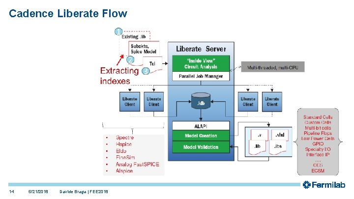
Cadence Liberate Flow 14 5/21/2018 Davide Braga | FEE 2018

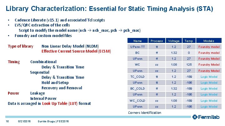
Library Characterization: Essential for Static Timing Analysis (STA) • • • Cadence Liberate (v 15. 1) and associated Tcl scripts LVS/QRC extraction of the cells Script to modify the model name (nch nch_mac, pch_mac) Foundry and custom model files Type of library Non Linear Delay Model (NLDM) Effective Current Source Model (ECSM) Timing Combinational Delay & Transition Time Sequential Delay & Transition Time Hold and Setup Recovery and Removal Power Leakage Internal Power Data is arranged in Look Up Table (LUT) format Name Process Voltage Temp Models UPenn-TT tt 1. 2 27 Foundry model BC ff 1. 32 0 Foundry model UPenn ff 1. 2 27 Foundry Model WC ss 1. 08 125 Foundry Model UPenn ss 1. 2 27 Foundry Model TC_COLD tt 1. 2 -189 Logix Model UPenn tt 1. 2 -186 Logix Model BC_COLD ff 1. 32 -189 Logix Model UPenn ff 1. 2 -186 Logix Model WC_COLD ss 1. 08 -189 Logix Model UPenn ss 1. 2 -186 Logix Model Corners Identification 15 5/21/2018 Davide Braga | FEE 2018

LVDS Transmitter and Receiver for liquid Argon • Designed to comply with LVDS standard (2. 5 V thick oxide transistors), but also to operate reliably down to VDD=1. 8 V • Programmable output current • Non-minimum length transistors for lifetime operation at liquid argon temperature (89 K) • Include level shifters to interface to 1. 2 V core voltage Both Tx and Rx have been prototyped and proven to work at both room and LAr temperatures, but have yet to be stress tested and characterized. In this prototype, Rx and Tx are linked through a I 2 C slave block, which limits the data rates. A dedicated test structure has been manufactured and is expected soon. 16 5/21/2018 Davide Braga | FEE 2018

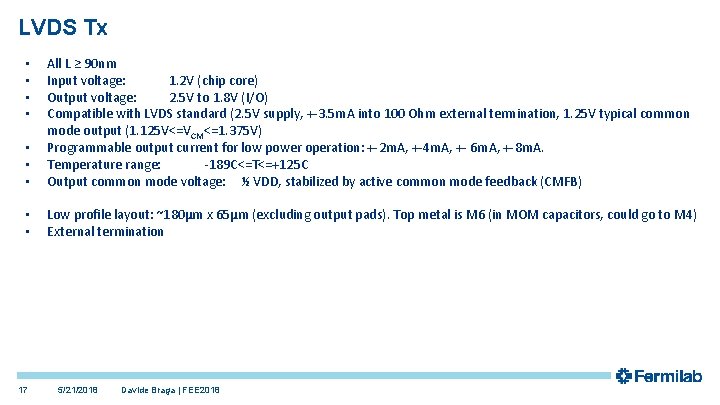
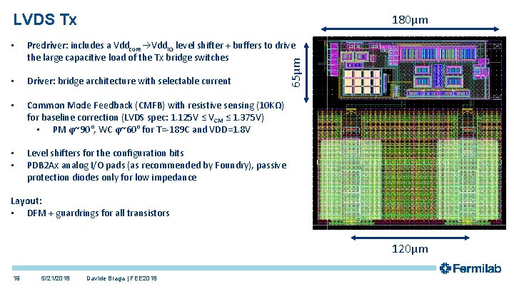
LVDS Tx • • • All L ≥ 90 nm Input voltage: 1. 2 V (chip core) Output voltage: 2. 5 V to 1. 8 V (I/O) Compatible with LVDS standard (2. 5 V supply, +-3. 5 m. A into 100 Ohm external termination, 1. 25 V typical common mode output (1. 125 V<=VCM<=1. 375 V) Programmable output current for low power operation: +-2 m. A, +-4 m. A, +- 6 m. A, +-8 m. A. Temperature range: -189 C<=T<=+125 C Output common mode voltage: ½ VDD, stabilized by active common mode feedback (CMFB) • • Low profile layout: ~180µm x 65µm (excluding output pads). Top metal is M 6 (in MOM capacitors, could go to M 4) External termination • • 17 5/21/2018 Davide Braga | FEE 2018

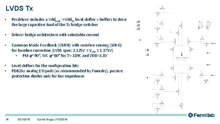
LVDS Tx • Predriver: includes a Vddcore Vdd. IO level shifter + buffers to drive the large capacitive load of the Tx bridge switches • Driver: bridge architecture with selectable current • Common Mode Feedback (CMFB) with resistive sensing (10 KΩ) for baseline correction (LVDS spec: 1. 125 V ≤ VCM ≤ 1. 375 V) • PM ϕ~90°, WC ϕ~60° for T=-189 C and VDD=1. 8 V • • Level shifters for the configuration bits PDB 2 Ax analog I/O pads (as recommended by Foundry), passive protection diodes only for low impedance 18 5/21/2018 Davide Braga | FEE 2018

LVDS Tx 180µm Predriver: includes a Vddcore Vdd. IO level shifter + buffers to drive the large capacitive load of the Tx bridge switches • Driver: bridge architecture with selectable current • Common Mode Feedback (CMFB) with resistive sensing (10 KΩ) for baseline correction (LVDS spec: 1. 125 V ≤ VCM ≤ 1. 375 V) • PM ϕ~90°, WC ϕ~60° for T=-189 C and VDD=1. 8 V • • Level shifters for the configuration bits PDB 2 Ax analog I/O pads (as recommended by Foundry), passive protection diodes only for low impedance 65µm • Layout: • DFM + guardrings for all transistors 120µm 19 5/21/2018 Davide Braga | FEE 2018

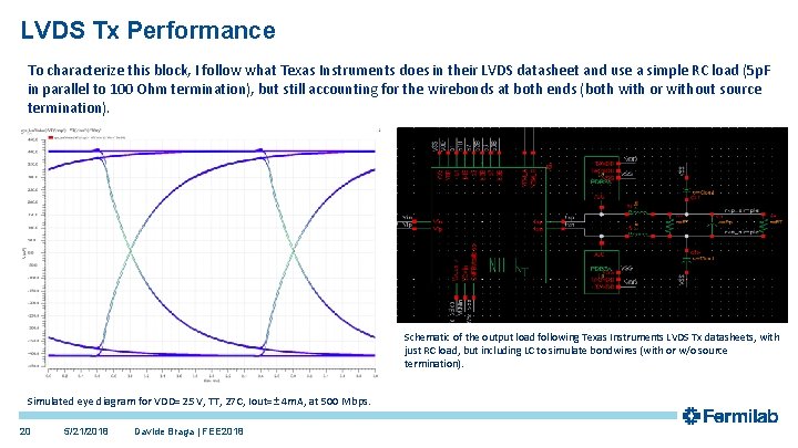
LVDS Tx Performance To characterize this block, I follow what Texas Instruments does in their LVDS datasheet and use a simple RC load (5 p. F in parallel to 100 Ohm termination), but still accounting for the wirebonds at both ends (both with or without source termination). Schematic of the output load following Texas Instruments LVDS Tx datasheets, with just RC load, but including LC to simulate bondwires (with or w/o source termination). Simulated eye diagram for VDD=2. 5 V, TT, 27 C, Iout=± 4 m. A, at 500 Mbps. 20 5/21/2018 Davide Braga | FEE 2018

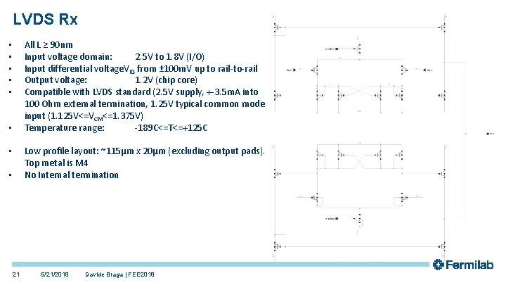
LVDS Rx All L ≥ 90 nm Input voltage domain: 2. 5 V to 1. 8 V (I/O) Input differential voltage. VID from ± 100 m. V up to rail-to-rail Output voltage: 1. 2 V (chip core) Compatible with LVDS standard (2. 5 V supply, +-3. 5 m. A into 100 Ohm external termination, 1. 25 V typical common mode input (1. 125 V<=VCM<=1. 375 V) Temperature range: -189 C<=T<=+125 C • • • Low profile layout: ~115µm x 20µm (excluding output pads). Top metal is M 4 No Internal termination • • 21 5/21/2018 Davide Braga | FEE 2018

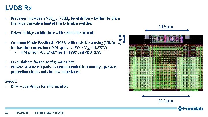
LVDS Rx Predriver: includes a Vddcore Vdd. IO level shifter + buffers to drive the large capacitive load of the Tx bridge switches • Driver: bridge architecture with selectable current • Common Mode Feedback (CMFB) with resistive sensing (10 KΩ) for baseline correction (LVDS spec: 1. 125 V ≤ VCM ≤ 1. 375 V) • PM ϕ~90°, WC ϕ~60° for T=-189 C and VDD=1. 8 V • • Level shifters for the configuration bits PDB 2 Ax analog I/O pads (as recommended by Foundry), passive protection diodes only for low impedance 115µm 20µm • Layout: • DFM + guardrings for all transistors 120µm 22 5/21/2018 Davide Braga | FEE 2018

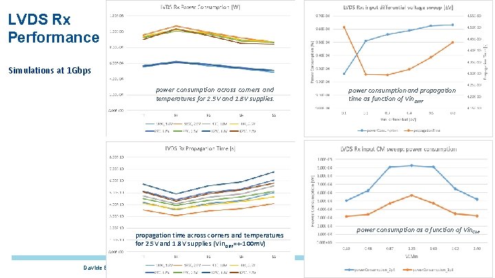
LVDS Rx Performance Simulations at 1 Gbps power consumption across corners and temperatures for 2. 5 V and 1. 8 V supplies. propagation time across corners and temperatures for 2. 5 V and 1. 8 V supplies (Vin. DIFF=+-100 m. V) Davide Braga 23| FEE 2018 5/21/2018 power consumption and propagation time as function of Vin. DIFF. power consumption as a function of Vin. CM.

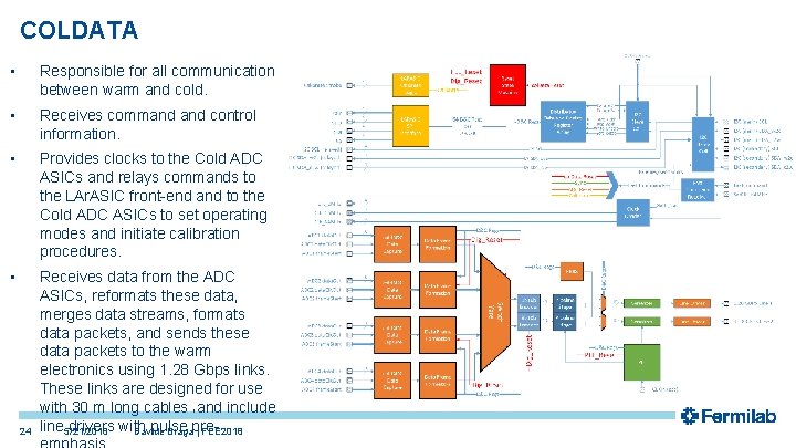
COLDATA • Responsible for all communication between warm and cold. • Receives command control information. • Provides clocks to the Cold ADC ASICs and relays commands to the LAr. ASIC front-end and to the Cold ADC ASICs to set operating modes and initiate calibration procedures. • Receives data from the ADC ASICs, reformats these data, merges data streams, formats data packets, and sends these data packets to the warm electronics using 1. 28 Gbps links. These links are designed for use with 30 m long cables and include line 5/21/2018 drivers with pulse Davide Bragapre| FEE 2018 1 24

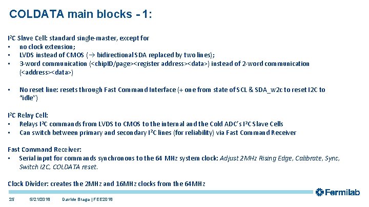
COLDATA main blocks - 1: I 2 C Slave Cell: standard single-master, except for • no clock extension; • LVDS instead of CMOS ( bidirectional SDA replaced by two lines); • 3 -word communication (<chip. ID/page><register address><data>) instead of 2 -word communication (<address><data>) • No reset line: resets through Fast Command Interface (+ one from state of SCL & SDA_w 2 c to reset I 2 C to “idle”) I 2 C Relay Cell: • Relays I 2 C commands from LVDS to CMOS to the internal and the Cold ADC’s I 2 C Slave Cells • Can switch between primary and secondary I 2 C lines (for reliability) via Fast Command Receiver: • Serial input for commands synchronous to the 64 MHz system clock: Adjust 2 MHz Rising Edge, Calibrate, Sync, Switch I 2 C, COLDATA reset. Clock Divider: creates the 2 MHz and 16 MHz clocks from the 64 MHz 25 5/21/2018 Davide Braga | FEE 2018

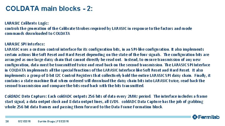
COLDATA main blocks - 2: LARASIC Calibrate Logic: controls the generation of the Calibrate Strobes required by LARASIC in response to the factors and mode commands downloaded to COLDATA LARASIC SPI Interface: LARASIC uses a custom control interface for its configuration bits, in an SPI-like configuration. It also implements certain actions like Soft Reset and Hard Reset depending on the state of the four signals. The configuration bits are arranged as one large daisy chain that cannot directly be read out. Instead, to ensure transmission of any new configuration, data must be transmitted twice and read back on the second transmission. The LARASIC SPI Interface in COLDATA implements all the special functions of the LARASIC Interface like Soft Reset and Hard Reset. It also implements a group of 8 -bit I 2 C Control Registers that collectively hold the entire LARASIC SPI daisy chain. Finally, it contains a state machine that when ordered will download the daisy chain bits into LARASIC twice, read back the second transmission and compare the bits read back with the bits transmitted. Cold. ADC Data Capture: Each cold. ADC outputs 256 bits of data every 2 MHz period. The interface includes a frame start signal, a data output clock and 8 data output lines, all LVDS. cold. ADC Data Capture has the job of grabbing whole 256 bit data frames and passing them forward to the Data Frame Formation block. 26 5/21/2018 Davide Braga | FEE 2018

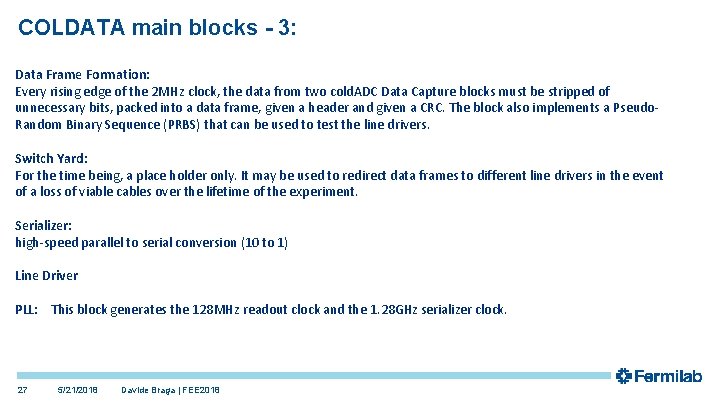
COLDATA main blocks - 3: Data Frame Formation: Every rising edge of the 2 MHz clock, the data from two cold. ADC Data Capture blocks must be stripped of unnecessary bits, packed into a data frame, given a header and given a CRC. The block also implements a Pseudo. Random Binary Sequence (PRBS) that can be used to test the line drivers. Switch Yard: For the time being, a place holder only. It may be used to redirect data frames to different line drivers in the event of a loss of viable cables over the lifetime of the experiment. Serializer: high-speed parallel to serial conversion (10 to 1) Line Driver PLL: This block generates the 128 MHz readout clock and the 1. 28 GHz serializer clock. 27 5/21/2018 Davide Braga | FEE 2018

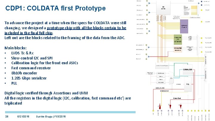
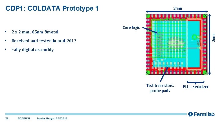
CDP 1: COLDATA first Prototype To advance the project at a time when the specs for COLDATA were still changing, we designed a prototype chip with all the blocks certain to be included in the final full chip. Left out are the blocks related to the framing of the data from the ADC. Main blocks: • LVDS Tx & Rx • Slow-control I 2 C and SPI • Calibration logic for the front end ASICs • Fast command receiver • 8 b 10 b encoder • 1. 285 Gbps serializer • PLL Digital logic verified through Assertions and UVM All the registers in the digital logic (I 2 C, calibration, fast command etc’) are triplicated 28 5/21/2018 Davide Braga | FEE 2018

CDP 1: COLDATA Prototype 1 2 x 2 mm, 65 nm 9 metal • Received and tested in mid-2017 • Fully digital assembly Core logic 2 mm • 2 mm Test transistors, probe pads 29 5/21/2018 Davide Braga | FEE 2018 PLL + serializer

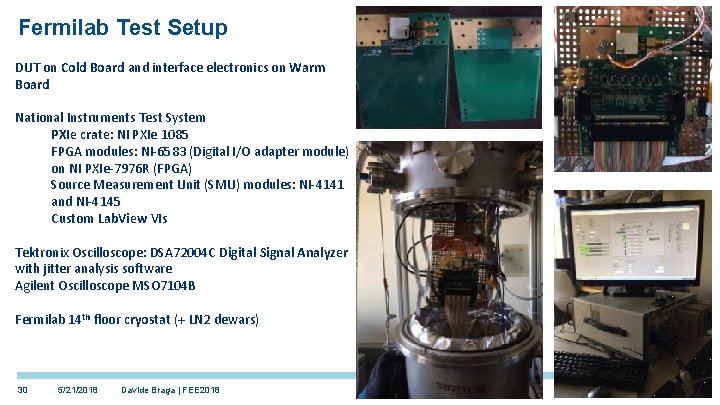
Fermilab Test Setup DUT on Cold Board and interface electronics on Warm Board National Instruments Test System PXIe crate: NI PXIe 1085 FPGA modules: NI-6583 (Digital I/O adapter module) on NI PXIe-7976 R (FPGA) Source Measurement Unit (SMU) modules: NI-4141 and NI-4145 Custom Lab. View VIs Tektronix Oscilloscope: DSA 72004 C Digital Signal Analyzer with jitter analysis software Agilent Oscilloscope MSO 7104 B Fermilab 14 th floor cryostat (+ LN 2 dewars) 30 5/21/2018 Davide Braga | FEE 2018

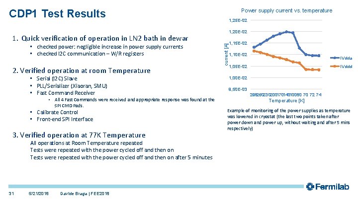
Power supply current vs. temperature CDP 1 Test Results 1, 25 E-02 1, 20 E-02 • checked power: negligible increase in power supply currents • checked I 2 C communication – W/R registers 2. Verified operation at room Temperature • Serial (I 2 C) Slave • PLL/Serializer (Xiaoran, SMU) • Fast Command Receiver • All 4 Fast Commands were received and appropriate response was found at the SPI CMD Pads. • Calibrate Control • Front-end SPI Interface 3. Verified operation at 77 K Temperature All operations at Room Temperature repeated Tests were repeated with the power cycled off and then on after 5 minutes 31 5/21/2018 Davide Braga | FEE 2018 current [A] 1. Quick verification of operation in LN 2 bath in dewar 1, 15 E-02 1, 10 E-02 IVdda 1, 05 E-02 IVddd 1, 00 E-02 9, 50 E-03 29826023020017014010080 70 72 74 Temperature [K] Example of monitoring of the power supplies as temperature was lowered in cryostat (the last two points taken after power down and power up, without waiting and after 5 mins respectively)

Conclusions and Future Developments • • • 32 COLDATA designed in 65 nm CMOS using “cold” transistor models based on data collected by members of the FNAL, BNL, and SMU ASIC groups. A special library of standard cells, based on these models and using a minimum channel length of 90 nm, was developed by members of the FNAL and UPENN groups, to eliminate the risk posed by the hot carrier effect. Both the models and the standard cell library can be made available upon request, provided the NDA with Foundry is in place. Fermilab could manage and maintain such library in a centralized database. The key circuit elements of COLDATA, including the control interface and the PLL and serializer, were prototyped and tested successfully in 2017. The serializer and the PLL have been extensively characterized. All other blocks were also proven functional at both room and LAr temperatures. A test structure for speed and stress tests of the LVDS Tx and Rx is expected soon Submission of COLDATA is expected later this year. 5/21/2018 Davide Braga | FEE 2018

Acknowledgements • Fermilab: Jim Hoff, Sandeep Miryala, Scott Holm, Grzegorz Deptuch, Alpana Shenai, Albert Dyer, Terri Shaw, David Christian • Southern Methodist University (PLL + serializer): Ping Gui, Xiaoran Wang, Tianwei Liu • University of Pennsylvania (library characterization): Mitch Newcomer, Nandor Dressnandt, Paul Keener 33 5/21/2018 Davide Braga | FEE 2018