RF Multiplexing Transmitting and Receiving Unit EE 413


- Slides: 29
RF Multiplexing Transmitting and Receiving Unit EE 413 Final Report By Adam Halstead and Michael Pfetsch
Problem and Solution Problem: There a limited number of frequency bands that can be allocated for sending information over long distances n Solution: Devise a system that enables the transmission of multiple sources of information over a single RF carrier frequency n
Description Digitize analog information from several sources n Multiplex multiple sources to form one source for transmission n Transmit multiplexed source using frequency modulation n Receive frequency modulated signal n Separate single source into its original sources n Convert signal back to analog and output to user n
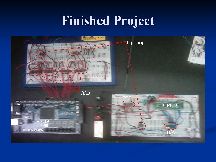
Finished Project Op-amps A/D PLL CPLD FPGA D/A
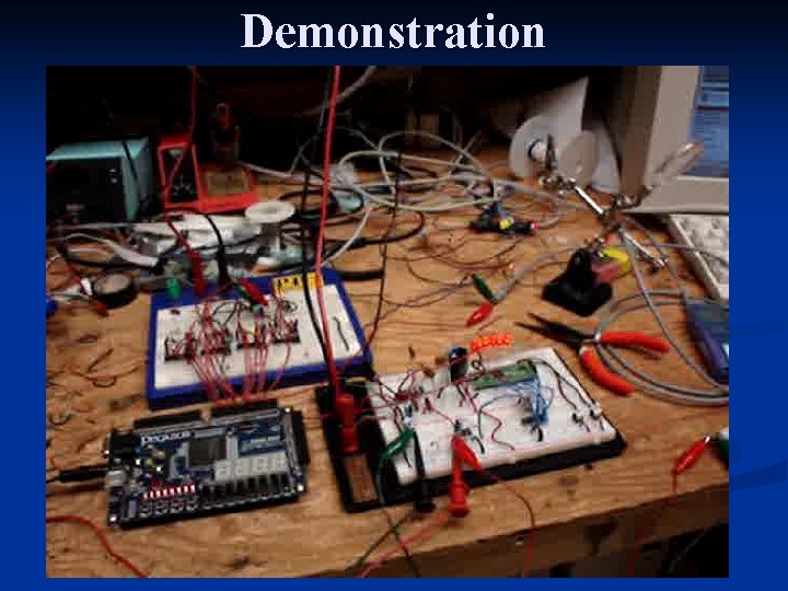
Demonstration
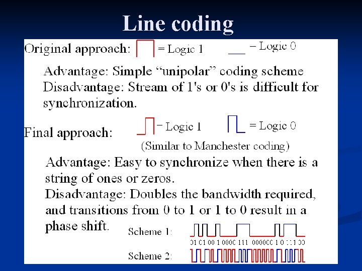
Results n n Successful multiplexing and de-multiplexing of 4 analog audio sources Successful construction of phase locked loop circuit Successful construction of an FM transmitter Could not synchronize transmitter and receiver using phase lock loop n n n Used direct clock connection for final demonstration Tried several different line coding schemes Bandwidth of transmitter/receiver limited to 75 k. Hz n inadequate for transmission rate of 330 kbps
Applications Surround sound radio/television streams: eg. : Front-left, front-right, rear-left, rear-right n Multilingual broadcasts eg. : Cantonese, Hindi, Arabic, English n Two stereo music streams of different genres: eg. : Beethoven’s 9 th Symphony and “I did it” by Dave Matthews Band n Four simultaneous talk radio shows: eg. : health, auto mechanics, poetry, politics n
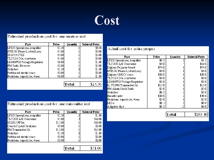
Cost
Transmission Protocol
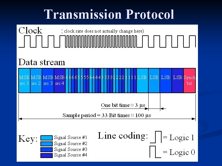
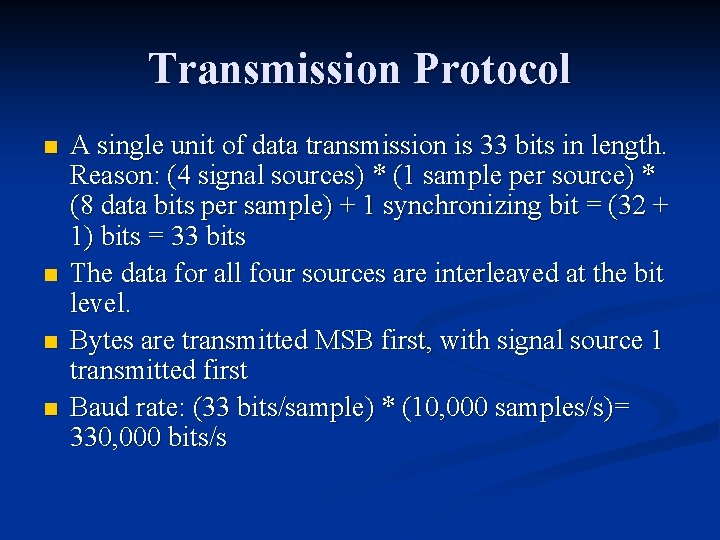
Transmission Protocol n n A single unit of data transmission is 33 bits in length. Reason: (4 signal sources) * (1 sample per source) * (8 data bits per sample) + 1 synchronizing bit = (32 + 1) bits = 33 bits The data for all four sources are interleaved at the bit level. Bytes are transmitted MSB first, with signal source 1 transmitted first Baud rate: (33 bits/sample) * (10, 000 samples/s)= 330, 000 bits/s
Line coding
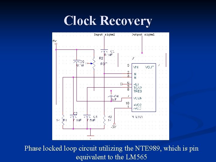
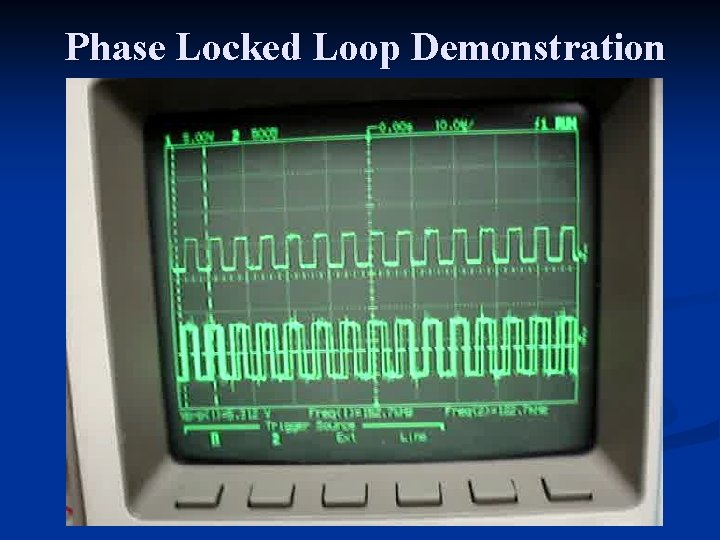
Clock Recovery Phase locked loop circuit utilizing the NTE 989, which is pin equivalent to the LM 565
Phase Locked Loop Demonstration
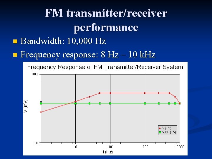
FM transmitter/receiver performance Bandwidth: 10, 000 Hz n Frequency response: 8 Hz – 10 k. Hz n
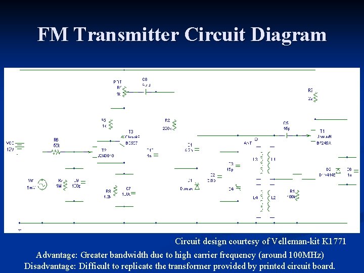
FM Transmitter Circuit Diagram Circuit design courtesy of Velleman-kit K 1771 Advantage: Greater bandwidth due to high carrier frequency (around 100 MHz) Disadvantage: Difficult to replicate the transformer provided by printed circuit board.
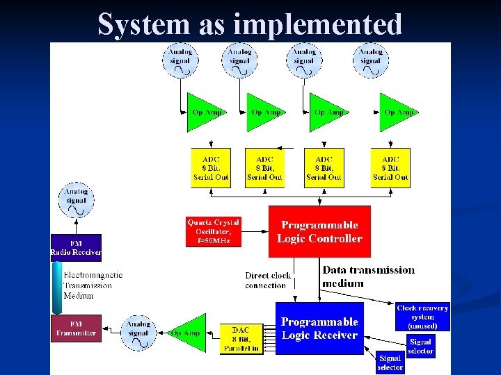
System as implemented
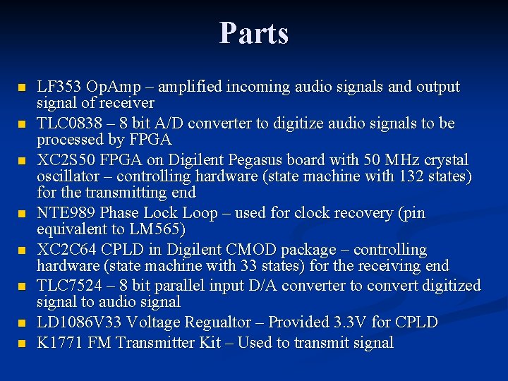
Parts n n n n LF 353 Op. Amp – amplified incoming audio signals and output signal of receiver TLC 0838 – 8 bit A/D converter to digitize audio signals to be processed by FPGA XC 2 S 50 FPGA on Digilent Pegasus board with 50 MHz crystal oscillator – controlling hardware (state machine with 132 states) for the transmitting end NTE 989 Phase Lock Loop – used for clock recovery (pin equivalent to LM 565) XC 2 C 64 CPLD in Digilent CMOD package – controlling hardware (state machine with 33 states) for the receiving end TLC 7524 – 8 bit parallel input D/A converter to convert digitized signal to audio signal LD 1086 V 33 Voltage Regualtor – Provided 3. 3 V for CPLD K 1771 FM Transmitter Kit – Used to transmit signal
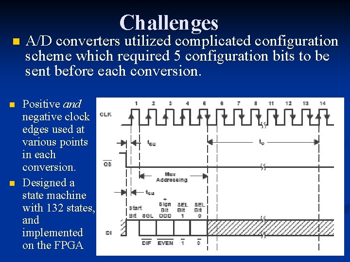
Challenges n n n A/D converters utilized complicated configuration scheme which required 5 configuration bits to be sent before each conversion. Positive and negative clock edges used at various points in each conversion. Designed a state machine with 132 states, and implemented on the FPGA
Challenges n Interfacing a 3. 3 V FPGA with 5 V A/D converters FPGA is 5 V Compliant n Configured I/O pins for TTL signal standard n Used high impedance state for logic 1 n Output pins of FPGA connected to 5 V through 10 kΩ pull up resistors n
Future Work Solve problem encountered in clock recovery with phase locked loop, eliminating need for separate clock connection. n Wireless transmission using TRF-24 G transceiver to provide enough bandwidth for higher quality audio signal. n Increase the number of multiplexed signals, by adding more A/D converters and changing the programmable logic controller. n Utilize digital audio compression/decompression n
References n n n Clark, Jeremy and Mcneil, Kyle James. “Experiment to view T 1 clock recovery”. Retrieved April 12, 2005, from “http: //www. picotech. com/experiments/t 1_clock_recovery/”. Liu, Pao-Lo. “Signal Generation and Conditioning” lecture notes. Retrieved April 4, 2005, from “http: //www. ee. buffalo. edu/faculty/paololiu/413/sigen. ppt”. Tomasi, Wayne. Electronic Communications Systems: Fundamentals Through Advanced, Fifth Edition. Upper Saddle River, New Jersey: Pearson Education, Inc. , 2004.
Questions?
End of show
Extra Slides
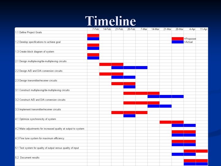
Timeline
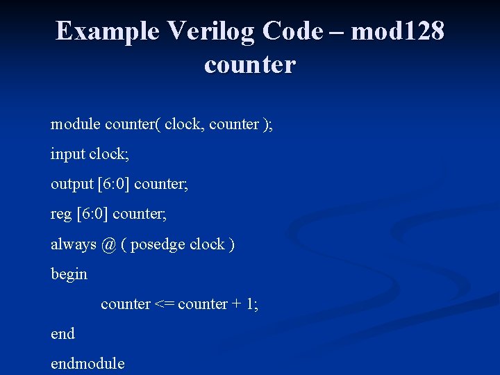
Example Verilog Code – mod 128 counter module counter( clock, counter ); input clock; output [6: 0] counter; reg [6: 0] counter; always @ ( posedge clock ) begin counter <= counter + 1; endmodule
Programmable Logic Devices n n n Complex Programmable Logic Devices (CPLD’s): Typically have 32 to 512 macrocells, each containing combinational logic and a flip flop. Field Programmable Gate Arrays (FPGA’s): A more recent technology, capable of realizing more complicated designs than CPLD’s. Verilog HDL: Hardware description language used to abstractly define a digital system. Useful for implementing a design on a CPLD or an FPGA, although basic schematic design may still be used.
Work Plan 1. 0 Project scope and approach 1. 1 Define project goals 1. 2 Develop specifications to achieve goal 1. 3 Create block diagram of system 2. 0 Design system 2. 1 Design multiplexing/de-multiplexing circuits 2. 2 Design A/D and D/A conversion circuits 2. 3 Design transmitter/receiver circuits 3. 0 Construction 3. 1 Construct multiplexing/de-multiplexing circuits 3. 2 Construct A/D and D/A conversion circuits 3. 3 Implement transmitter/receiver circuits
Work Plan continued 4. 0 Optimization 4. 1 Optimize synchronization of system 4. 2 Make adjustments for increased quality at output to system 4. 3 Fine tune system for maximum efficiency 5. 0 Testing and Documentation 5. 1 Test system for quality of output versus quality of input 5. 2 Document results