Characterization of the Apsel 4 well chip analog
- Slides: 18

Characterization of the Apsel 4 well chip analog front-end fabricated with INMAPS technology S. Zuccaa, c, L. Rattia, c V. Reb, c, G. Traversib, c a. Università b. Università degli Studi di Pavia degli Studi di Bergamo c. INFN Pavia 4 th Super. B Collaboration Meeting- 1 th June 2012

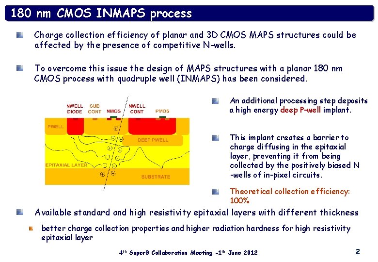
180 nm CMOS INMAPS process Charge collection efficiency of planar and 3 D CMOS MAPS structures could be affected by the presence of competitive N-wells. To overcome this issue the design of MAPS structures with a planar 180 nm CMOS process with quadruple well (INMAPS) has been considered. An additional processing step deposits a high energy deep P-well implant. This implant creates a barrier to charge diffusing in the epitaxial layer, preventing it from being collected by the positively biased N -wells of in-pixel circuits. Theoretical collection efficiency: 100% Available standard and high resistivity epitaxial layers with different thickness better charge collection properties and higher radiation hardness for high resistivity epitaxial layer 4 th Super. B Collaboration Meeting -1 th June 2012 2

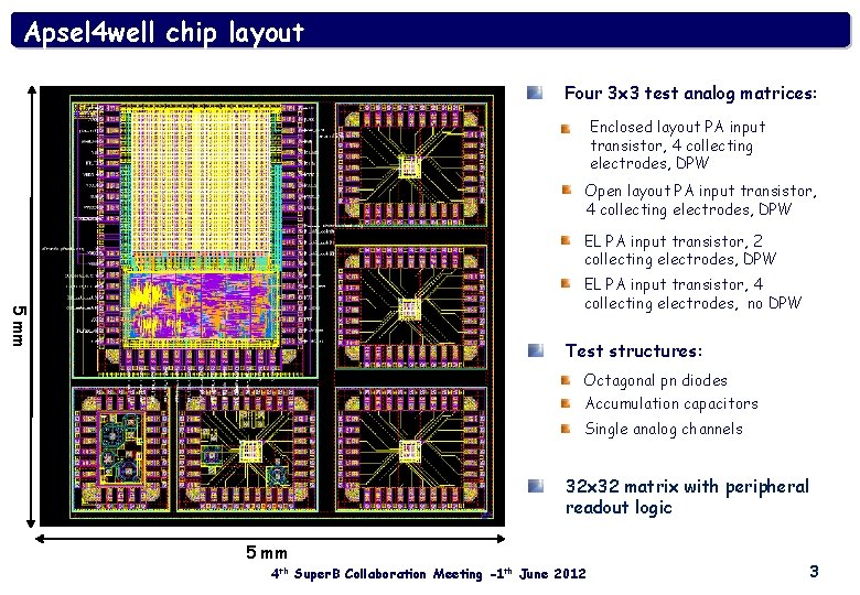
Apsel 4 well chip layout Four 3 x 3 test analog matrices: Enclosed layout PA input transistor, 4 collecting electrodes, DPW Open layout PA input transistor, 4 collecting electrodes, DPW EL PA input transistor, 2 collecting electrodes, DPW 5 mm EL PA input transistor, 4 collecting electrodes, no DPW Test structures: Octagonal pn diodes Accumulation capacitors Single analog channels 32 x 32 matrix with peripheral readout logic 5 mm 4 th Super. B Collaboration Meeting -1 th June 2012 3

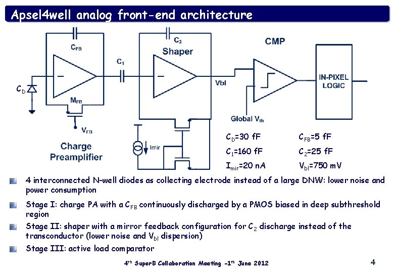
Apsel 4 well analog front-end architecture CD CD=30 f. F CFB=5 f. F C 1=160 f. F C 2=25 f. F Imir=20 n. A Vbl=750 m. V 4 interconnected N-well diodes as collecting electrode instead of a large DNW: lower noise and power consumption Stage I: charge PA with a CFB continuously discharged by a PMOS biased in deep subthreshold region Stage II: shaper with a mirror feedback configuration for C 2 discharge instead of the transconductor (lower noise and Vbl dispersion) Stage III: active load comparator 4 th Super. B Collaboration Meeting -1 th June 2012 4

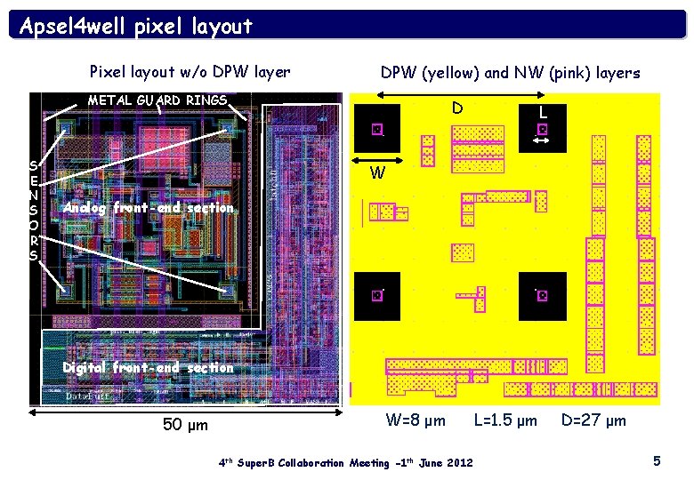
Apsel 4 well pixel layout Pixel layout w/o DPW layer DPW (yellow) and NW (pink) layers METAL GUARD RINGS S E N S O R S D L W Analog front-end section Digital front-end section 50 μm W=8 μm 4 th Super. B Collaboration Meeting -1 th June 2012 L=1. 5 μm D=27 μm 5

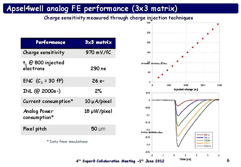
Apsel 4 well analog FE performance (3 x 3 matrix) Charge sensitivity measured through charge injection techniques Performance 3 x 3 matrix Charge sensitivity 970 m. V/f. C tp @ 800 injected electrons 290 ns ENC (CD = 30 f. F) 26 e- INL (@ 2000 e-) 2% Current consumption* 10 μA/pixel Analog Power consumption* 18 μW/pixel Pixel pitch 50 μm * Data from simulations 4 th Super. B Collaboration Meeting -1 th June 2012 6

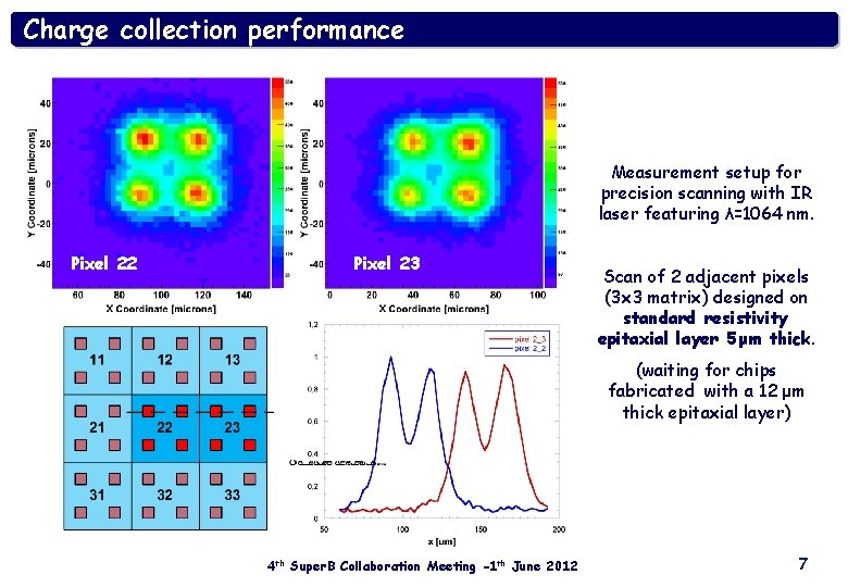
Charge collection performance Measurement setup for precision scanning with IR laser featuring λ=1064 nm. Pixel 22 Pixel 23 Scan of 2 adjacent pixels (3 x 3 matrix) designed on standard resistivity epitaxial layer 5 μm thick. (waiting for chips fabricated with a 12 μm thick epitaxial layer) 4 th Super. B Collaboration Meeting -1 th June 2012 7

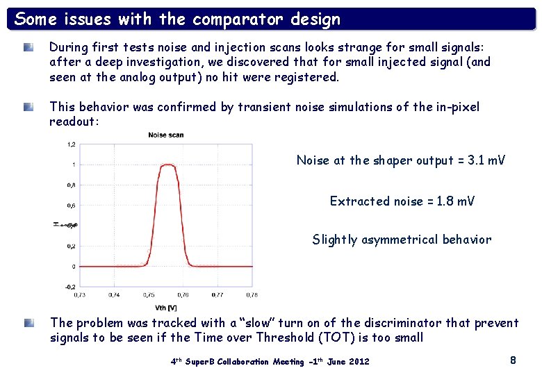
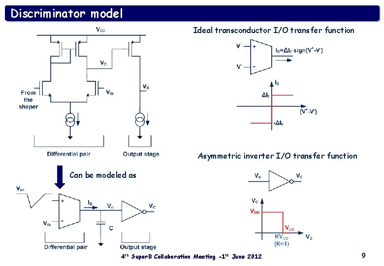
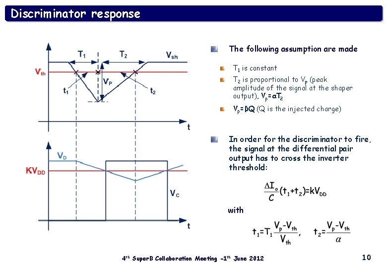
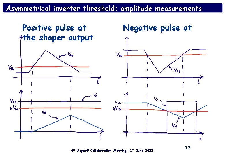
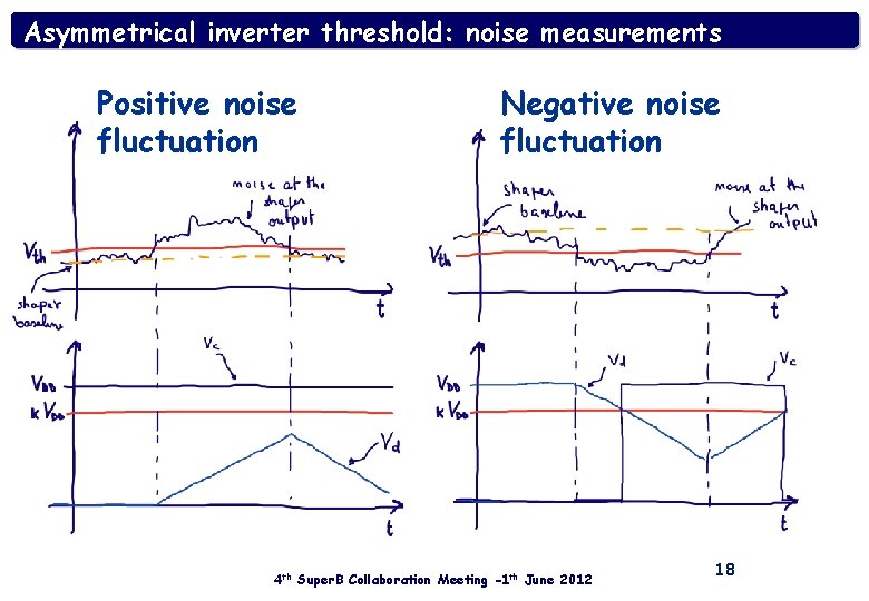
Some issues with the comparator design During first tests noise and injection scans looks strange for small signals: after a deep investigation, we discovered that for small injected signal (and seen at the analog output) no hit were registered. This behavior was confirmed by transient noise simulations of the in-pixel readout: Noise at the shaper output = 3. 1 m. V Extracted noise = 1. 8 m. V Slightly asymmetrical behavior The problem was tracked with a “slow” turn on of the discriminator that prevent signals to be seen if the Time over Threshold (TOT) is too small. 4 th Super. B Collaboration Meeting -1 th June 2012 8

Discriminator model Ideal transconductor I/O transfer function Asymmetric inverter I/O transfer function Can be modeled as 4 th Super. B Collaboration Meeting -1 th June 2012 9

Discriminator response The following assumption are made T 1 is constant T 2 is proportional to Vp (peak amplitude of the signal at the shaper output), Vp=αT 2 Vp=βQ (Q is the injected charge) In order for the discriminator to fire, the signal at the differential pair output has to cross the inverter threshold: with 4 th Super. B Collaboration Meeting -1 th June 2012 10

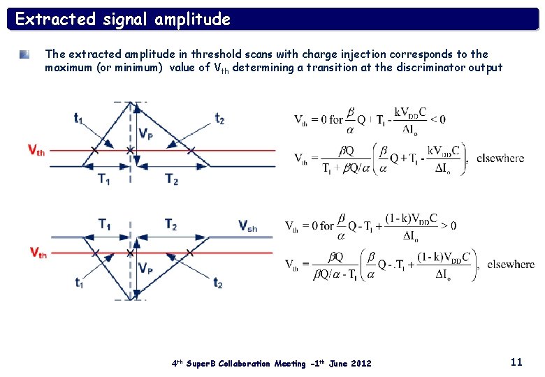
Extracted signal amplitude The extracted amplitude in threshold scans with charge injection corresponds to the maximum (or minimum) value of Vth determining a transition at the discriminator output 4 th Super. B Collaboration Meeting -1 th June 2012 11

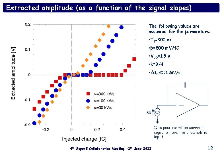
Extracted amplitude (as a function of the signal slopeα) The following values are assumed for the parameters: • T 1=300 ns • β=800 m. V/f. C • VDD=1. 8 V • k=3/4 • ΔIo/C=1 MV/s Q is positive when current signal enters the preamplifier input 4 th Super. B Collaboration Meeting -1 th June 2012 12

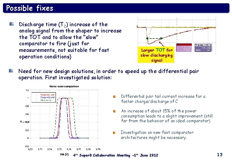
Possible fixes Discharge time (T 2) increase of the analog signal from the shaper to increase the TOT and to allow the “slow” comparator to fire (just for measurements, not suitable for fast operation conditions) Larger TOT for slow discharging signal Need for new design solutions, in order to speed up the differential pair operation. First investigated solution: Differential pair tail current increase for a faster charge/discharge of C An increase of about 15% of the power consumption leads to a slight improvement (still far from the behavior of an ideal comparator) Investigation on new fast comparator architectures might be necessary. 4 th Super. B Collaboration Meeting -1 th June 2012 13

Conclusion and perspectives Apsel 4 well chip fabricated with the INMAPS process (standard resistivity 5 μm thick epitaxial layer) has been characterized in terms of analog channel performance and charge collection properties. Good analog FE performance (noise=26 e- with 18 μW power consumption). Laser characterization showed poor charge collection properties (thin and low res. epi layer). Noise and injection scan highlighted some issues with the comparator (fixed by increasing the discharge time of the signal at the shaper output). FUTURE ACTIVITIES: Full characterization of chip with standard and high res. 12 μm thick epitaxial layer (delivery expected in 2 or 3 weeks). Fix the comparator for next submissions. Charge collection performance evaluation of structures with 2 N-well diodes and without deep P-well (for comparison). Radiation hardness tests. 4 th Super. B Collaboration Meeting -1 th June 2012 14

Backup slides 4 th Super. B Collaboration Meeting -1 th June 2012 15

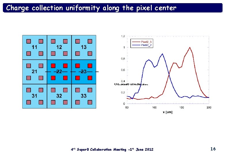
Charge collection uniformity along the pixel center 4 th Super. B Collaboration Meeting -1 th June 2012 16

Asymmetrical inverter threshold: amplitude measurements Positive pulse at the shaper output Negative pulse at the shaper output 4 th Super. B Collaboration Meeting -1 th June 2012 17

Asymmetrical inverter threshold: noise measurements Positive noise fluctuation Negative noise fluctuation 4 th Super. B Collaboration Meeting -1 th June 2012 18