Chapter 8 Counter 1 Introduction A counter a


 is applied to the clock")


 binary counter. 9")


 Design a counter with the irregular binary count sequence shown in the state")
 Figure A shows the schematic for a 3 -bit counter. Assuming that")

,")


- Slides: 52
Chapter 8 Counter 1
Introduction • A counter – a group of flip-flops connected together to perform counting operations ( flip-flops are used to construct counters) • The number of flip-flops used and the way in which they are connected determine the number of states (modulus). • Two broad categories according to the way they are clocked: 1) Asynchronous counter 2) Synchronous counter 2
Asynchronous Counter Operation • The term asynchronous refers to events that do not have a fixed time relationship with each other and, generally, do not occur at the same time. • An asynchronous counter is one in which the flip flops (FF) within the counter do not change states at exactly the same time because they do not have a common clock pulse. 3
Asynchronous Counter Operation • Asynchronous binary counter – 2 -bit asynchronous binary counter – 3 -bit asynchronous binary counter – 4 -bit asynchronous binary counter • Asynchronous decade counter 4
A 2 -bit asynchronous binary counter The clock (CLK) is applied to the clock input (C) of only the first flip flop which is always the least significant bit (LSB). The second flip flop is triggered by the output of the first flip flop. Because of the inherent propagation delay time through a flip flop, a transition of the input clock pulse (CLK) and a transition of the output of FF 0 can never occur at the exactly the same time. Therefore, the two flip flop are never simultaneously triggered, so the counter operation is asynchronous. 5
The Binary State Sequence for a 2 -bit Binary Counter 6
3 -bit asynchronous binary counter and its timing diagram for one cycle 7
The Binary State Sequence for a 3 -bit Binary Counter CLOCK PULSE Initially 1 2 3 4 5 6 7 8 (recycles) Q 2 0 0 0 Q 1 0 0 1 Q 0 0 1 1 1 1 0 0 1 1 0 1 0 8
Propagation delays in a 3 -bit asynchronous (ripple-clocked) binary counter. 9
Asynchronous Decade Counters • The modulus of a counter is the number of unique states through which the counter will sequence. • The maximum possible number of states (max modulus) is 2 n. Where n is the number of flip-flops. • Counter can also be designed to have a number of states in their sequence that is less than the maximum of 2 n. The resulting sequence is called truncated sequence. • Counter with ten states are called decade counter. • To obtain a truncated sequence it is necessary to force the counter to recycle before going through all of its possible states. 10
An Asynchronously Clocked Decade Counter with Asynchronous recycling 11
Example Show an asynchronous counter can be implemented having a modulus of twelve with a straight binary sequence from 0000 through 1011. 12
The 74 LS 93 4 bit asynchronous binary counter The 74 LS 93 is an example of a specific integrated circuit asynchronous counter. It consists of a single flip flop and a 3 bit asynchronous counter. It can be used as divide by 2 device if only the single flip flop is used, or it can be used as a modulus 8 counter if only the 3 bit counter portion is used. This device also provide gated reset inputs, (RO(1) and RO(2)). 13 When both of these inputs are HIGH, the counter is reset to 0000 state.
Synchronous Counter Operation Synchronous refers to events that have a fixed time relationship with each other. A synchronous counter is one in which all the flip flops in the counter are clocked at the same time by a common clock pulse. • Synchronous binary counters – 2 -bit counter – 3 -bit counter – 4 -bit counter • Synchronous BCD decade counter 14
A 2 bit Synchronous Binary Counter 15
16
Timing details for the 2 -bit synchronous counter operation (the propagation delays of both flip-flops are assumed to be equal) 17
18
Binary State Sequence for a 3 Bit Binary Counter 19
A 4 bit Synchronous Binary Counter 20 Points where the AND gate outputs are HIGH are indicated by the shaded areas.
A 4 bit Synchronous Decade Counter 21
States of a 4 bit Synchronous Decade Counter 22
DESIGN OF SYNCHRONOUS COUNTER General sequential circuit – combinational logic section + memory section (FF) At any given time, memory is in a state – present state (Q 0, Q 1, …. . , Qp) Memory will advance to a next state on a clock pulse – determine by condition on the excitation lines (Y 0, Y 1, …, Yp) General clocked sequential circuit.
DESIGN OF SYNCHRONOUS COUNTER Steps used in the design of sequential circuit: Step 1: State diagram ØDiagram that shows all the transition of states when clock triggered. ØSpecify the counter sequence and draw a state diagram ØAmount of FF needed are also determine depending on the bit 000 100 011 001 010 LSB MSB
DESIGN OF SYNCHRONOUS COUNTER Step 2: Next-State Table ØTable that list all the present state along with next state ØDerive a next-state table from the state diagram Present State 000 100 011 0 0 1 QC QB QA Present State QC QB QA 0 0 0 1 001 010 Next State 1 1 0 0 1 0 Next State QC QB QA 0 0 1 0 1 0 0
DESIGN OF SYNCHRONOUS COUNTER Step 3: Transition Table ØDevelop a transition table showing the flip-flop inputs required for each transition. ØThe transition table is always the same for a given type of flip-flop
DESIGN OF SYNCHRONOUS COUNTER Transition table for JK Flip Flop Output Transitions QN Flip-flop Inputs QN+1 J K 0 0 0 X 0 1 1 X 1 0 X 1 1 1 X 0 QN = present state of FF (before a clock pulse) QN+1 = next state (after a clock pulse) X = Don’t care
DESIGN OF SYNCHRONOUS COUNTER Transition table for D Flip Flop Output Transitions QN Flip-flop Inputs QN+1 D 0 0 1 1 1
DESIGN OF SYNCHRONOUS COUNTER Transition table for SR Flip Flop Output Transitions QN Flip-flop Inputs QN+1 S R 0 0 0 X 0 1 1 0 0 1 1 1 X 0
DESIGN OF SYNCHRONOUS COUNTER Output Transitions QN Flip-flop Inputs QN+1 J K 0 0 0 X 0 1 1 X 1 0 X 1 1 1 X 0 Present State Next State FFC 000 100 001 011 FFB FFA QC QB Q JC KC JB KB JA K A A 0 0 0 1 1 0 0 0 X X 0 1 X X 1 0 0 1 1 0 X X 0 1 X 010
DESIGN OF SYNCHRONOUS COUNTER Step 4: Karnaugh Map ØTransfer the J and K states from the transition table to Kmaps ØThere is a K-map for each input of each flip-flop. Step 5: Logic Expression for FF inputs Ø Group the K-map cells to generate and derive the logic expression for each flip-flop input. Step 6: Counter Implementation Ø Implement the expressions with combinational logic, and combine with the flip-flops to create the counter.
DESIGN OF SYNCHRONOUS COUNTER Steps used in the design of sequential circuit: 1. Specify the counter sequence and draw a state diagram 2. Derive a next-state table from the state diagram – table that listed all the present state along with next state table 3. Develop a transition table showing the flip-flop inputs required for each transition. The transition table is always the same for a given type of flip-flop 4. Transfer the J and K states from the transition table to K-maps. There is a K-map for each input of each flip-flop. 5. Group the K-map cells to generate and derive the logic expression for each flip-flop input. 6. Implement the expressions with combinational logic, and combine with the flip-flops to create the counter.
DESIGN OF SYNCHRONOUS COUNTER Example: Design 3 -bit Gray code counter by using JK flip-flop. Step 1: State Diagram State diagram for a 3 -bit Gray code counter.
DESIGN OF SYNCHRONOUS COUNTER Step 2: Next state table Next-state table for a 3 -bit Gray code counter. Next State Present State Q 2 Q 1 Q 0 0 0 0 1 0 1 1 0 1 1 1 1 0 0 0 0 0
DESIGN OF SYNCHRONOUS COUNTER Step 3: Transition Table Output Transitions QN QN QN+1 J K 0 0 0 X 0 1 1 X 1 0 X 1 1 1 X 0 : present state QN+1: next state X: Don’t care Flip-flop Inputs
DESIGN OF SYNCHRONOUS COUNTER Step 3: Transition Table Present State Next State FF 2 FF 1 FF 0 Q 2 Q 1 Q 0 J 2 K 2 J 1 K 1 J 0 K 0 0 0 1 0 X 1 X 0 0 1 1 0 X 1 X X 0 0 0 1 1 1 1 0 0 1 1 0 1 1 1 0 0 0 1 X X X 0 0 0 1 X 0 X 0 X 1 0 X X 0 1 X
DESIGN OF SYNCHRONOUS COUNTER Step 4: Karnaugh Map
DESIGN OF SYNCHRONOUS COUNTER Step 5: Logic Expression for FF inputs
DESIGN OF SYNCHRONOUS COUNTER Step 6: Counter Implementation
Exercise(a) Design a counter with the irregular binary count sequence shown in the state diagram of figure below. Use J-K flip flops 40
Exercise (b) Figure A shows the schematic for a 3 -bit counter. Assuming that the initial stage/count = 000, Find its counting sequence. Figure A 41
Example : State diagram for a 3 -bit up/down Gray code counter.
Task: Design 3 -bit up/down Gray code counter. If input Y is LOW (0), it will count down and if Y is HIGH, it will count up Step 1: State Diagram
Step 2: Next-state table
Step 3: Transition Table Present Y Next FFC FFB FFA State QC QB QA QC QB Q JC KC JB KB J K A 0 0 1 1 0 1 0 1 0 0 0 1 1 0 1 1 1 0 0 1 0 0 0 X X X X 0 0 1 1 0 0 X X 0 1 X X 0 0 A A 0 X 1 X 0 X 1
Present Y Next State FFC FFB FFA State QC QB QA QC QB Q JC KC JB KB J K A 0 0 1 1 0 1 0 1 1 1 1 1 0 0 1 1 1 0 0 1 1 0 0 1 0 X X X X 1 0 0 1 X X 0 0 X X 0 1 A A 1 X 0 X 1 X 0
Step 4: Karnaugh Map JC MAP KC MAP
JB MAP KB MAP
JA MAP KA MAP
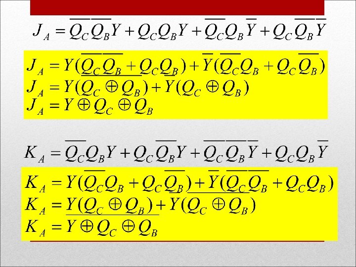
Step 5: Logic Expression for FF inputs
Step 6: Counter Implementation