Synchronous Counter Design Procedure 1 Describe a counter
 Describe a counter circuit in terms of its count")
Synchronous Counter Design Procedure 1) Describe a counter circuit in terms of its count sequence 2) Develop a state diagram from the given sequence 3) Develop a state table from the state diagram 4) Select type of Flip-flop (D or J-K) and create excitation table for the counter 5) Use K-map to derive the logic equations for flip-flop inputs 6) Implement the logic circuit to produce the specified sequence of states 7) Analyze the counter to verify the design

Synchronous Counter Design Excitation table for D flip-flop Excitation table for J-K flip-flop State table in different format

Excitation Tables for various Flip-Flops q q Excitation tables are essentially state tables presented in a form that is suitable for design of synchronous counters Excitation tables are used to determine what the control inputs of each flip-flop (J and K or D) has to be in order for the flip-flop to make a transition from one state to the next

State Table for D Flip-Flop Present input D Present state Qt Next state Qt+1 0 0 0 1 0 1 1 1

Excitation Table for D Flip-Flop Present state Qt Next state Qt+1 Flip-flop input D 0 0 1 1 1

State Table for J-K Flip-Flop Present input Present state J K Qt Next state Qt+1 0 0 0 1 1 0 1 1 1 1 0

Excitation Table for J-K Flip-Flop Present state Qt Next state Qt+1 Flip-flop input J K 0 0 0 X 0 1 1 X 1 0 X 1 1 1 X 0

Homework: Excitation Table for S-R Flip-Flop Present state Qt Next state Qt+1 Flip-flop input S R
 Design a 2 -bit synchronous binary up counter")
1) Design a 2 -bit synchronous binary up counter
 State Table: The circuit will have two flip-flops ( FF 0 & FF")
3) State Table: The circuit will have two flip-flops ( FF 0 & FF 1) Present State Q 1 (t) Q 0 (t) Next State Q 1(t+1) Q 0 (t+1)
 State Table: The circuit will have two flip-flops ( FF 0 & FF")
3) State Table: The circuit will have two flip-flops ( FF 0 & FF 1) Present State Q 1 (t) Q 0 (t) Next State Q 1(t+1) Q 0 (t+1) 0 0 0 1 0 1 1 1 1 0 0
 Choose D flip-flop for our design Present State Q 1(t) Next State Q")
4) Choose D flip-flop for our design Present State Q 1(t) Next State Q 0(t) Q 1(t+1) Q 0(t+1) 0 0 0 1 0 1 1 1 1 0 0 Excitation table for counter F-F Inputs
 Choose D flip-flop for our design Present State Q 1(t) Next State Q")
4) Choose D flip-flop for our design Present State Q 1(t) Next State Q 0(t) Q 1(t+1) Q 0(t+1) F-F Inputs D 1 D 0 0 1 0 1 1 1 0 0 Excitation table for counter
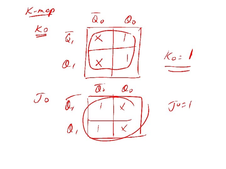
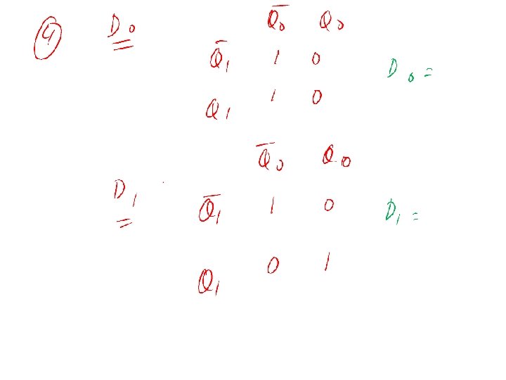
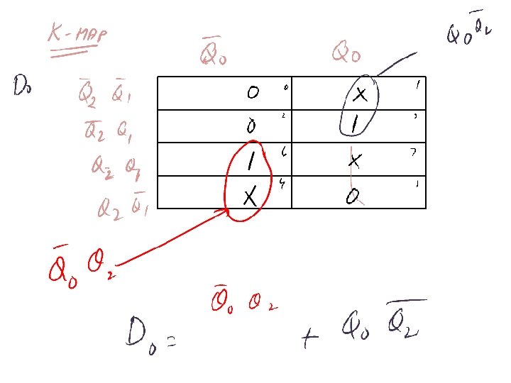
 K-map for D 0 and D 1 Excitation Equation for D 0 =")
5) K-map for D 0 and D 1 Excitation Equation for D 0 = Excitation Equation D 1 =
 K-map for D 0 and D 1 1 0 Excitation Equation for D")
5) K-map for D 0 and D 1 1 0 Excitation Equation for D 0 = Q 0 0 1 1 0 Excitation Equation D 1 = Q 0 O Q 1
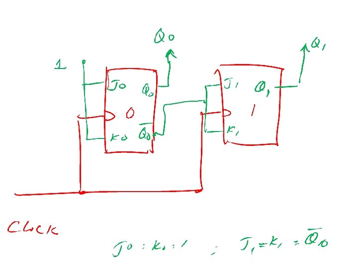
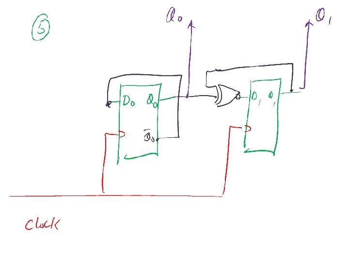
 Implement the logic circuit from the excitation equations")
6) Implement the logic circuit from the excitation equations

Homework: Redesign the 2 -bit up counter using J-K flip-flops
 flip-flops Present State")
Example: Design a 2 -bit down counter using J-K (or D) flip-flops Present State Q 1 (t) Q 0 (t) Next State Q 1(t+1) Q 0 (t+1) 0 0 1 1 0 0 1 1 0
 Q 0 (t) Next State Q 1(t+1)")
Choose Flip-flops Present State Q 1 (t) Q 0 (t) Next State Q 1(t+1) Q 0 (t+1) J 1 K 1 J 0 K 0 0 0 1 1 1 x 0 1 0 0 0 x x 1 1 0 0 1 x 1 1 1 0 x 1 Flip-Flop Inputs

K 1

Example: Use D flip-flops to design a synchronous counter that counts in the following order: 0, 2, 6, 3, 5, 0, 2, …. . Need 3 bit counter Unused states
 State diagram Since")
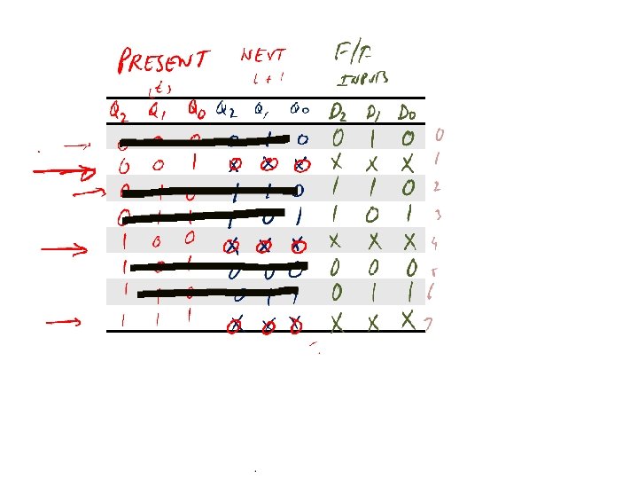
Example: Design a synchronous BCD up counter using J-K flip-flops 1) State diagram Since BCD is a 4 -bit code, the counter is 4 -bit in size. However, we only use the first 10 of the 16 possible states, so it is a modulus 10 counter. The six unused states can be treated as don’t care in the design. Decade counter
 State Table: The circuit will have four flip-flops Present State Q (t) Next")
3) State Table: The circuit will have four flip-flops Present State Q (t) Next State Q(t+1) Q 3 Q 2 Q 1 Q 0 0 0 0 0 1 0 0 0 1 1 0 1 0 0 0 1 0 1 0 1 1 0 0 1 1 1 1 0 0 0 1 0 0
 Choose J-K flip-flop for our design Present State Q (t) Next State Q(t+1)")
4) Choose J-K flip-flop for our design Present State Q (t) Next State Q(t+1) Q 3 Q 2 Q 1 Q 0 0 0 0 0 1 0 0 0 1 1 0 1 0 0 0 1 0 1 0 1 1 0 0 1 1 1 1 0 0 0 1 0 0 Excitation table for counter
 K-map simplification")
5) K-map simplification

74160 Synchronous BCD Counter

74160 o o CEP and CET must be high to count TC will go low when highest count is reached MR PE CET CEP Clk L X X X Reset H L X X Load H H Count H H L X No Change H H X L No Change
- Slides: 33