Chapter 18 Capacitive Circuits Topics Covered in Chapter
- Slides: 36

Chapter 18 Capacitive Circuits Topics Covered in Chapter 18 18 -1: Sine-Wave VC Lags i. C by 90 o 18 -2: XC and R in Series 18 -3: Impedance Z Triangle 18 -4: RC Phase-Shifter Circuit 18 -5: XC and R in Parallel © 2007 The Mc. Graw-Hill Companies, Inc. All rights reserved.

Topics Covered in Chapter 18 § 18 -6: RF and AF Coupling Capacitors § 18 -7: Capacitive Voltage Dividers § 18 -8: The General Case of Capacitive Current i. C Mc. Graw-Hill © 2007 The Mc. Graw-Hill Companies, Inc. All rights reserved.

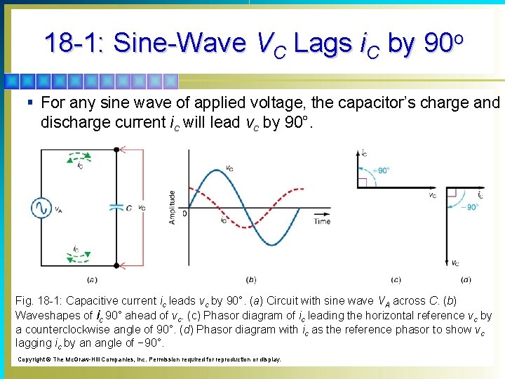
18 -1: Sine-Wave VC Lags i. C by 90 o § For any sine wave of applied voltage, the capacitor’s charge and discharge current ic will lead vc by 90°. Fig. 18 -1: Capacitive current ic leads vc by 90°. (a) Circuit with sine wave VA across C. (b) Waveshapes of ic 90° ahead of vc. (c) Phasor diagram of ic leading the horizontal reference vc by a counterclockwise angle of 90°. (d) Phasor diagram with ic as the reference phasor to show vc lagging ic by an angle of − 90°. Copyright © The Mc. Graw-Hill Companies, Inc. Permission required for reproduction or display.

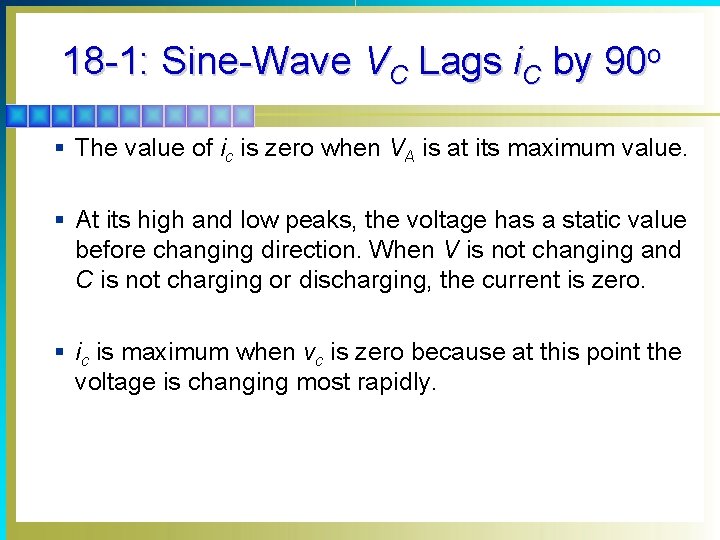
18 -1: Sine-Wave VC Lags i. C by 90 o § The value of ic is zero when VA is at its maximum value. § At its high and low peaks, the voltage has a static value before changing direction. When V is not changing and C is not charging or discharging, the current is zero. § ic is maximum when vc is zero because at this point the voltage is changing most rapidly.

18 -1: Sine-Wave VC Lags i. C by 90 o § ic and vc are 90° out of phase because the maximum value of one corresponds to the zero value of the other. § The 90° phase angle results because ic depends on the rate of change of vc. ic has the phase of dv/dt, not the phase of v. § The 90° phase between vc and ic is true in any sine wave ac circuit. For any XC, its current and voltage are 90° out of phase.

18 -1: Sine-Wave VC Lags i. C by 90 o § The frequency of vc and ic are always the same. § The leading phase angle only addresses the voltage across the capacitor. The current is still the same in all parts of a series circuit. In a parallel circuit, the voltage across the generator and capacitor are always the same, but both are 90° out of phase with ic.

18 -2: XC and R in Series § When a capacitor and a resistor are connected in series, the current is limited by both XC and R. § Each series component has its own series voltage drop equal to IR for the resistance and IXC for the capacitive reactance. § For any circuit combining XC and R in series, the following points are true: 1. The current is labeled I rather than IC, because I flows through all the series components.

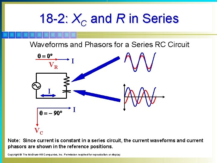
18 -2: XC and R in Series 2. The voltage across XC, labeled VC, can be considered an IXC voltage drop, just as we use VR for an IR voltage drop. 3. The current I through XC must lead VC by 90°, because this is the phase angle between the voltage and current for a capacitor. 4. The current I through R and its IR voltage drop are in phase. There is no reactance to sine-wave alternating current in any resistance. Therefore, I and IR have a phase angle of 0°.

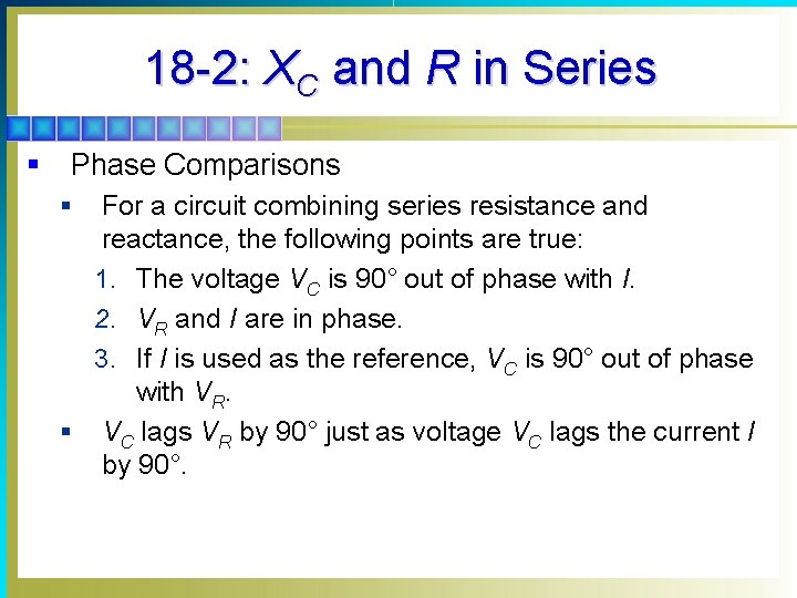
18 -2: XC and R in Series § Phase Comparisons For a circuit combining series resistance and reactance, the following points are true: 1. The voltage VC is 90° out of phase with I. 2. VR and I are in phase. 3. If I is used as the reference, VC is 90° out of phase with VR. § VC lags VR by 90° just as voltage VC lags the current I by 90°. §

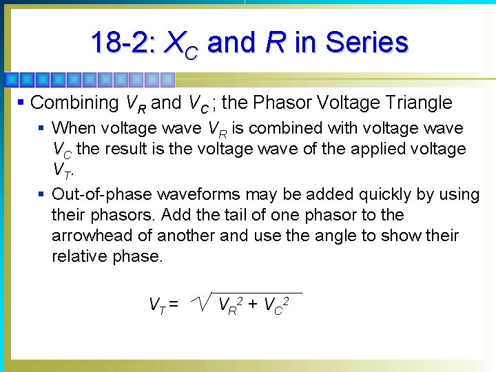
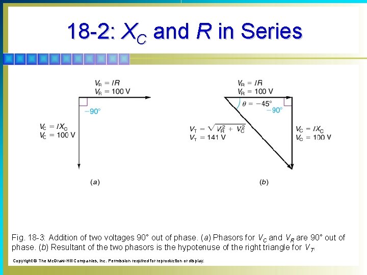
18 -2: XC and R in Series § Combining VR and VC ; the Phasor Voltage Triangle § When voltage wave VR is combined with voltage wave VC the result is the voltage wave of the applied voltage V T. § Out-of-phase waveforms may be added quickly by using their phasors. Add the tail of one phasor to the arrowhead of another and use the angle to show their relative phase. VT = V R 2 + V C 2

18 -2: XC and R in Series Fig. 18 -3: Addition of two voltages 90° out of phase. (a) Phasors for VC and VR are 90° out of phase. (b) Resultant of the two phasors is the hypotenuse of the right triangle for VT. Copyright © The Mc. Graw-Hill Companies, Inc. Permission required for reproduction or display.

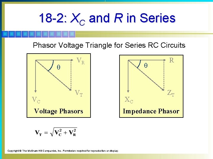
18 -2: XC and R in Series Phasor Voltage Triangle for Series RC Circuits q VC VR VT Voltage Phasors Copyright © The Mc. Graw-Hill Companies, Inc. Permission required for reproduction or display. q XC R ZT Impedance Phasor

18 -2: XC and R in Series Waveforms and Phasors for a Series RC Circuit q = 0 VR I I q = - 90 I VC Note: Since current is constant in a series circuit, the current waveforms and current phasors are shown in the reference positions. Copyright © The Mc. Graw-Hill Companies, Inc. Permission required for reproduction or display.

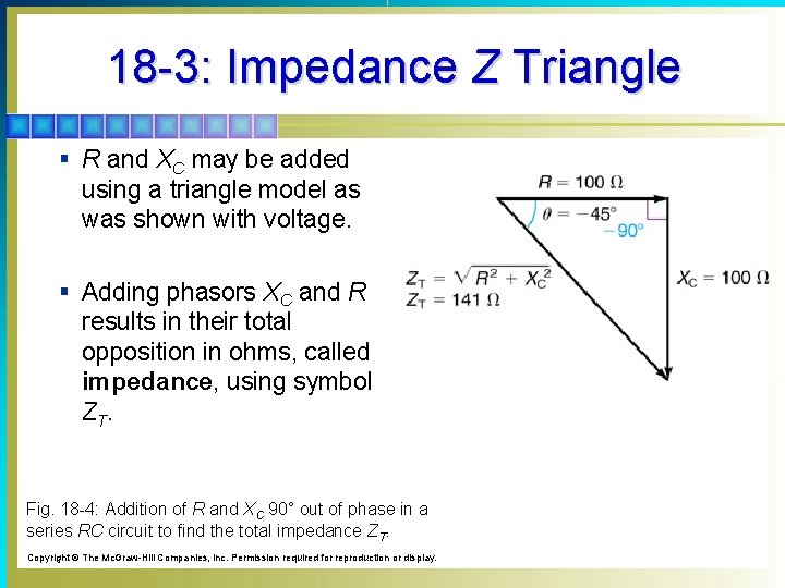
18 -3: Impedance Z Triangle § R and XC may be added using a triangle model as was shown with voltage. § Adding phasors XC and R results in their total opposition in ohms, called impedance, using symbol Z T. Fig. 18 -4: Addition of R and XC 90° out of phase in a series RC circuit to find the total impedance ZT. Copyright © The Mc. Graw-Hill Companies, Inc. Permission required for reproduction or display.

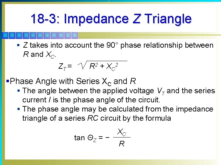
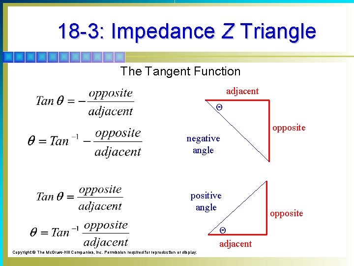
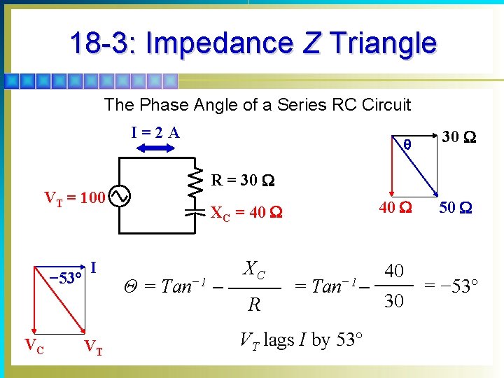
18 -3: Impedance Z Triangle § Z takes into account the 90° phase relationship between R and XC. ZT = R 2 + X C 2 §Phase Angle with Series XC and R § The angle between the applied voltage VT and the series current I is the phase angle of the circuit. § The phase angle may be calculated from the impedance triangle of a series RC circuit by the formula tan ΘZ = − XC R

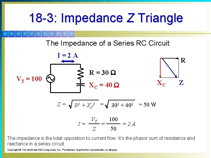
18 -3: Impedance Z Triangle The Impedance of a Series RC Circuit I=2 A R R = 30 W VT = 100 XC XC = 40 W Z= R 2 + XC 2 = I= VT Z = Z 302 + 402 = 50 W 100 50 =2 A The impedance is the total opposition to current flow. It’s the phasor sum of resistance and reactance in a series circuit Copyright © The Mc. Graw-Hill Companies, Inc. Permission required for reproduction or display.

18 -3: Impedance Z Triangle The Tangent Function adjacent Θ negative angle positive angle Θ adjacent Copyright © The Mc. Graw-Hill Companies, Inc. Permission required for reproduction or display. opposite

18 -3: Impedance Z Triangle The Phase Angle of a Series RC Circuit I=2 A − 53° VC VT 30 W 40 W 50 W R = 30 W VT = 100 I q XC = 40 W Θ= Tan− 1 - XC R = Tan− 1 - VT lags I by 53° 40 30 = − 53°

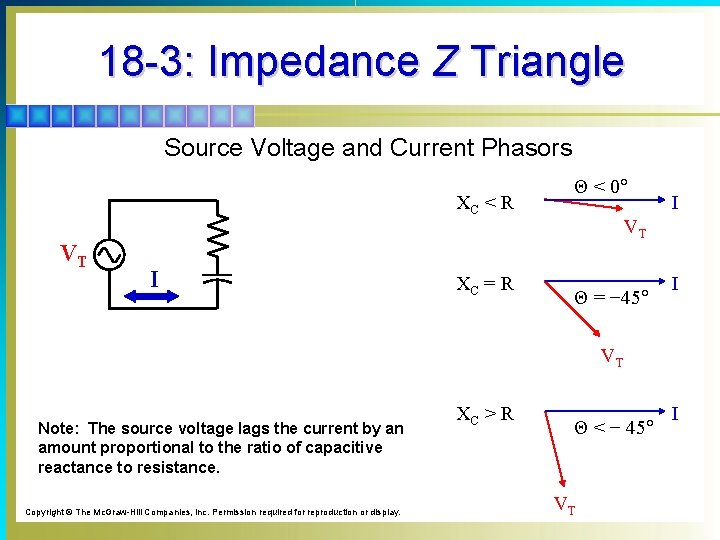
18 -3: Impedance Z Triangle Source Voltage and Current Phasors XC < R VT I XC = R Θ < 0 I VT Θ = − 45 I VT Note: The source voltage lags the current by an amount proportional to the ratio of capacitive reactance to resistance. Copyright © The Mc. Graw-Hill Companies, Inc. Permission required for reproduction or display. XC > R Θ < − 45 VT I

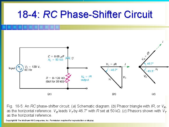
18 -4: RC Phase-Shifter Circuit § The RC phase-shift circuit is used to provide a voltage of variable phase to set the conduction time of semiconductors in power control circuits. § Output can be taken across R or C depending on desired phase shift with respect to VIN. § VR leads VT by an amount depending on the values of XC and R. § VC lags VT by an amount depending on the values of XC and R.

18 -4: RC Phase-Shifter Circuit Fig. 18 -5: An RC phase-shifter circuit. (a) Schematic diagram. (b) Phasor triangle with IR, or VR, as the horizontal reference. VR leads VT by 46. 7° with R set at 50 kΩ. (c) Phasors shown with VT as the horizontal reference. Copyright © The Mc. Graw-Hill Companies, Inc. Permission required for reproduction or display.

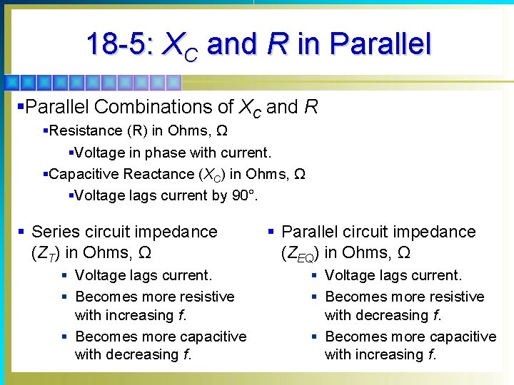
18 -5: XC and R in Parallel § The sine-wave ac charge and discharge currents for a capacitor lead the capacitor voltage by 90°. § The sine-wave ac voltage across a resistor is always in phase with its current. § The total sine-wave ac current for a parallel RC circuit always leads the applied voltage by an angle between 0° and 90°.

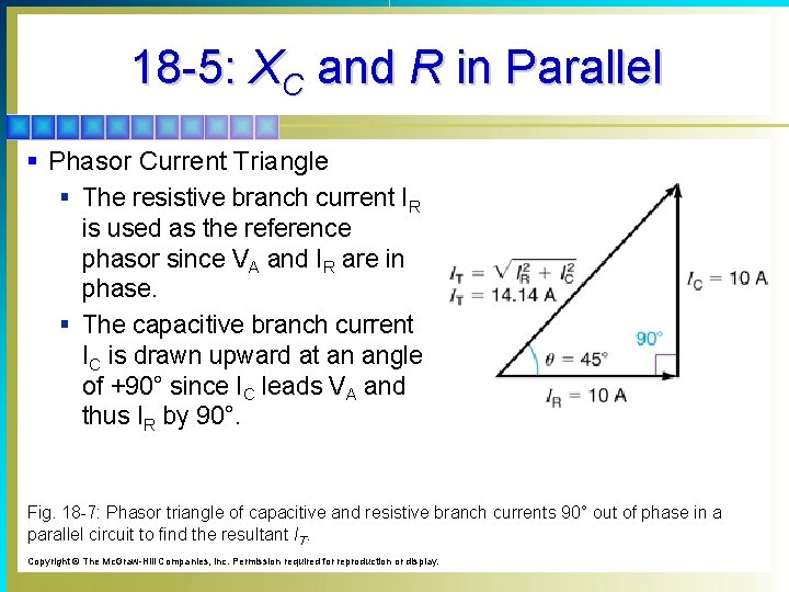
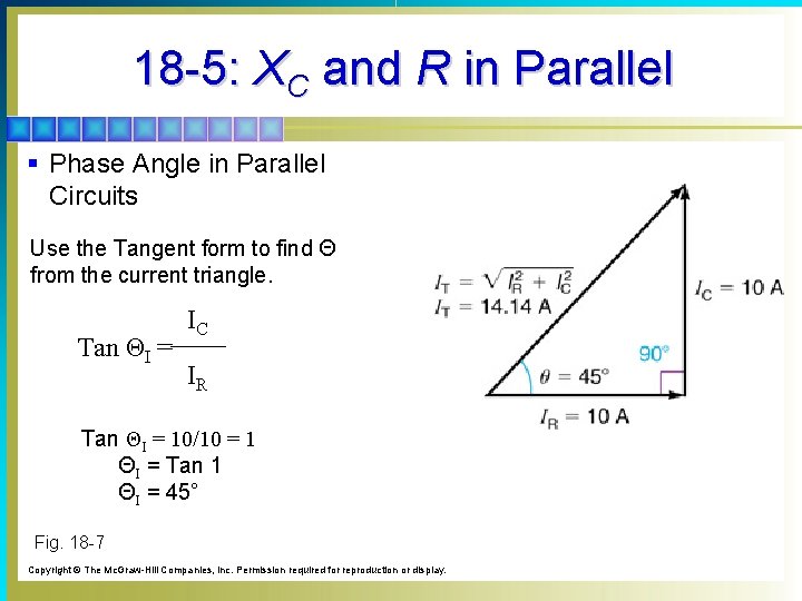
18 -5: XC and R in Parallel § Phasor Current Triangle § The resistive branch current IR is used as the reference phasor since VA and IR are in phase. § The capacitive branch current IC is drawn upward at an angle of +90° since IC leads VA and thus IR by 90°. Fig. 18 -7: Phasor triangle of capacitive and resistive branch currents 90° out of phase in a parallel circuit to find the resultant IT. Copyright © The Mc. Graw-Hill Companies, Inc. Permission required for reproduction or display.

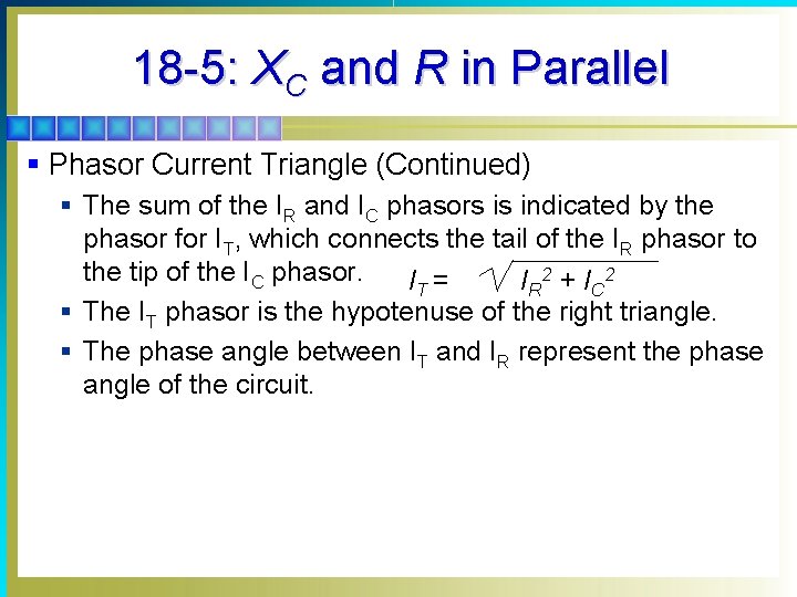
18 -5: XC and R in Parallel § Phasor Current Triangle (Continued) § The sum of the IR and IC phasors is indicated by the phasor for IT, which connects the tail of the IR phasor to the tip of the IC phasor. IT = I R 2 + I C 2 § The IT phasor is the hypotenuse of the right triangle. § The phase angle between IT and IR represent the phase angle of the circuit.

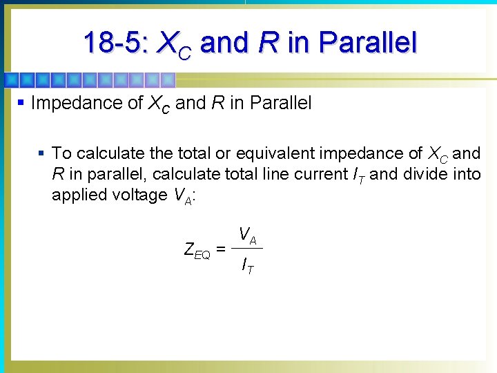
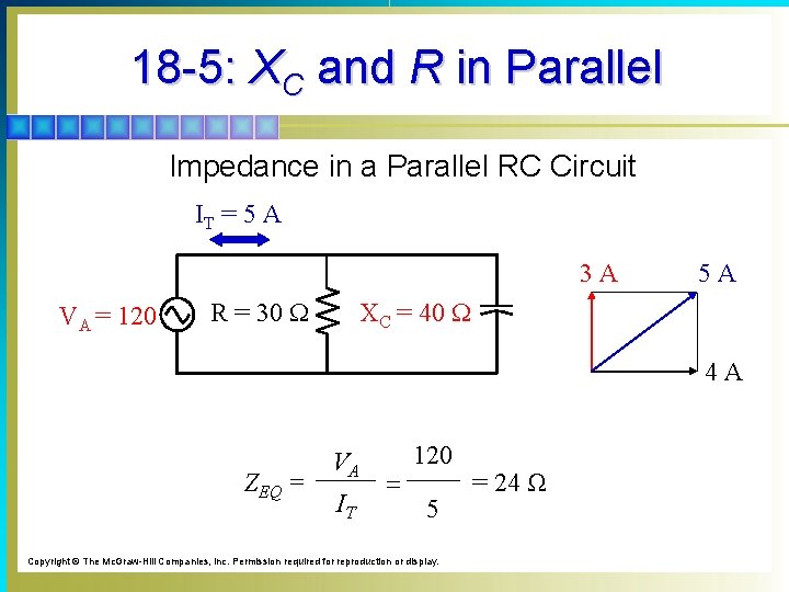
18 -5: XC and R in Parallel § Impedance of XC and R in Parallel § To calculate the total or equivalent impedance of XC and R in parallel, calculate total line current IT and divide into applied voltage VA: ZEQ = VA IT

18 -5: XC and R in Parallel Impedance in a Parallel RC Circuit IT = 5 A 3 A VA = 120 R = 30 W 5 A XC = 40 W 4 A ZEQ = VA IT = 120 5 Copyright © The Mc. Graw-Hill Companies, Inc. Permission required for reproduction or display. = 24 Ω

18 -5: XC and R in Parallel § Phase Angle in Parallel Circuits Use the Tangent form to find Θ from the current triangle. Tan ΘI = IC IR Tan ΘI = 10/10 = 1 ΘI = Tan 1 ΘI = 45° Fig. 18 -7 Copyright © The Mc. Graw-Hill Companies, Inc. Permission required for reproduction or display.

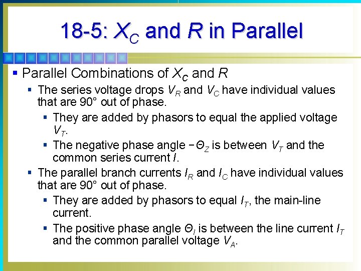
18 -5: XC and R in Parallel § Parallel Combinations of XC and R § The series voltage drops VR and VC have individual values that are 90° out of phase. § They are added by phasors to equal the applied voltage V T. § The negative phase angle −ΘZ is between VT and the common series current I. § The parallel branch currents IR and IC have individual values that are 90° out of phase. § They are added by phasors to equal IT, the main-line current. § The positive phase angle ΘI is between the line current IT and the common parallel voltage VA.

18 -5: XC and R in Parallel §Parallel Combinations of XC and R §Resistance (R) in Ohms, Ω §Voltage in phase with current. §Capacitive Reactance (XC) in Ohms, Ω §Voltage lags current by 90°. § Series circuit impedance (ZT) in Ohms, Ω § Voltage lags current. § Becomes more resistive with increasing f. § Becomes more capacitive with decreasing f. § Parallel circuit impedance (ZEQ) in Ohms, Ω § Voltage lags current. § Becomes more resistive with decreasing f. § Becomes more capacitive with increasing f.

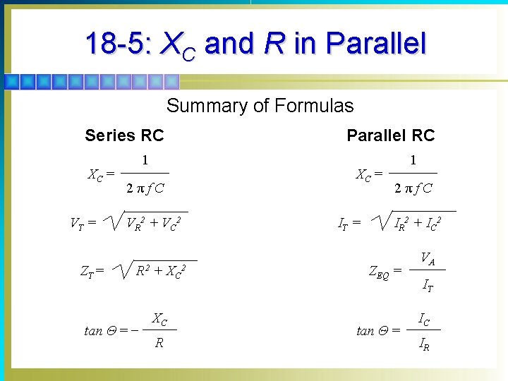
18 -5: XC and R in Parallel Summary of Formulas Series RC XC = VT = ZT = Parallel RC 1 XC = 2πf. C VR 2 + VC 2 R 2 tan Θ = − + XC 2 XC R IT = 1 2πf. C IR 2 + IC 2 ZEQ = tan Θ = VA IT IC IR

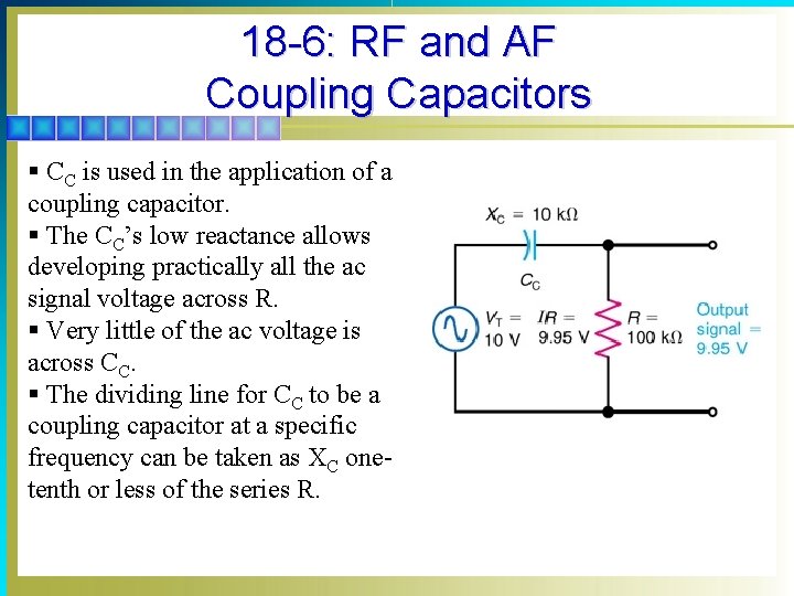
18 -6: RF and AF Coupling Capacitors § CC is used in the application of a coupling capacitor. § The CC’s low reactance allows developing practically all the ac signal voltage across R. § Very little of the ac voltage is across CC. § The dividing line for CC to be a coupling capacitor at a specific frequency can be taken as XC onetenth or less of the series R.

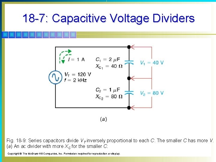
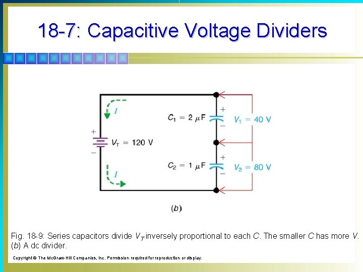
18 -7: Capacitive Voltage Dividers § When capacitors are connected in series across a voltage source, the series capacitors serve as a voltage divider. § Each capacitor has part of the applied voltage. § The sum of all the series voltage drops equals the source voltage. § The amount of voltage across each capacitor is inversely proportional to its capacitance.

18 -7: Capacitive Voltage Dividers Fig. 18 -9: Series capacitors divide VT inversely proportional to each C. The smaller C has more V. (a) An ac divider with more XC for the smaller C. Copyright © The Mc. Graw-Hill Companies, Inc. Permission required for reproduction or display.

18 -7: Capacitive Voltage Dividers Fig. 18 -9: Series capacitors divide VT inversely proportional to each C. The smaller C has more V. (b) A dc divider. Copyright © The Mc. Graw-Hill Companies, Inc. Permission required for reproduction or display.

18 -8: The General Case of Capacitive Current i. C § The capacitive charge and discharge current ic is always equal to C(dv/dt). § A sine wave of voltage variations for vc produces a cosine wave of current i. § Note that vc and ic have the same waveform, but they are 90° out of phase.

18 -8: The General Case of Capacitive Current i. C § XC is generally used for calculations in sine-wave circuits. § Since XC is 1/(2πf. C), the factors that determine the amount of charge and discharge current are included in f and C. § With a nonsinusoidal waveform for voltage vc, the concept of reactance cannot be used. (Reactance XC applies only to sine waves).