100 340 GHz Systems Transistors and Applications M


- Slides: 25

100 -340 GHz Systems: Transistors and Applications M. J. W. Rodwell 1, Y. Fang 1, J. Rode 1, 2, J. Wu 1, 3, B. Markman 1, S. T. Suran Brunelli 1, J. Klamkin 1, M Urteaga 4 1 University of California, Santa Barbara 2 Now with Intel 3 Now with Global. Foundries 4 Teledyne Scientific and Imaging 1

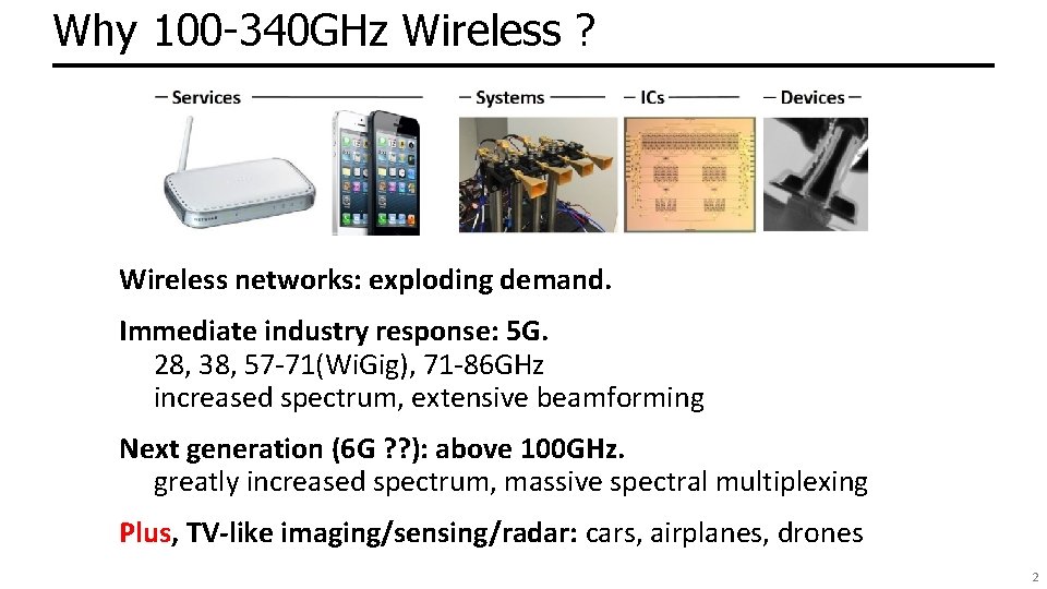
Why 100 -340 GHz Wireless ? Wireless networks: exploding demand. Immediate industry response: 5 G. 28, 38, 57 -71(Wi. Gig), 71 -86 GHz increased spectrum, extensive beamforming Next generation (6 G ? ? ): above 100 GHz. greatly increased spectrum, massive spectral multiplexing Plus, TV-like imaging/sensing/radar: cars, airplanes, drones 2

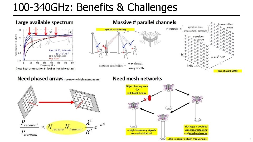
100 -340 GHz: Benefits & Challenges 3

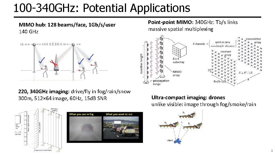
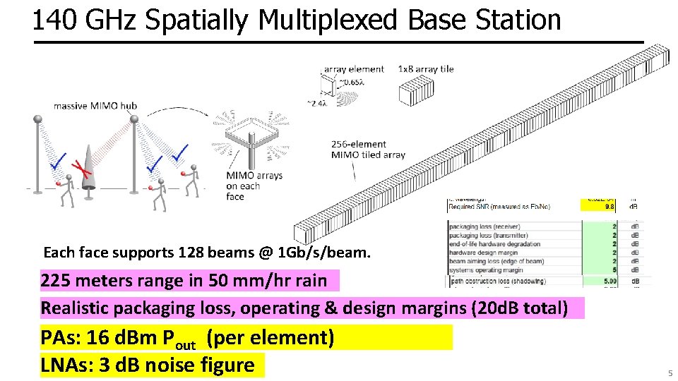
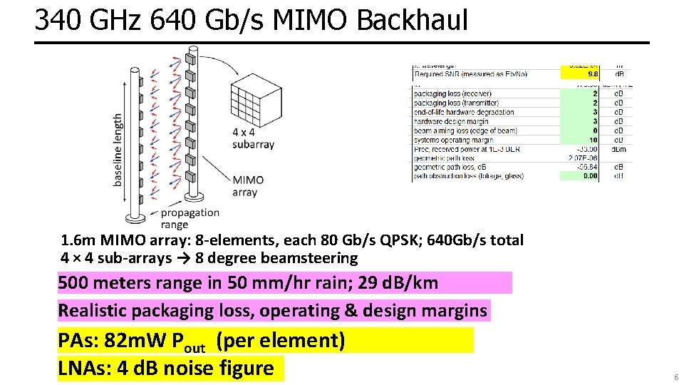
100 -340 GHz: Potential Applications MIMO hub: 128 beams/face, 1 Gb/s/user 140 GHz 220, 340 GHz imaging: drive/fly in fog/rain/snow 300 m, 512× 64 image, 60 Hz, 15 d. B SNR Point-point MIMO: 340 GHz: Tb/s links massive spatial multiplexing Ultra-compact imaging: drones unlike visible: image through fog/smoke/rain 4

140 GHz Spatially Multiplexed Base Station Each face supports 128 beams @ 1 Gb/s/beam. 225 meters range in 50 mm/hr rain Realistic packaging loss, operating & design margins (20 d. B total) PAs: 16 d. Bm Pout (per element) LNAs: 3 d. B noise figure 5

340 GHz 640 Gb/s MIMO Backhaul 1. 6 m MIMO array: 8 -elements, each 80 Gb/s QPSK; 640 Gb/s total 4 × 4 sub-arrays → 8 degree beamsteering 500 meters range in 50 mm/hr rain; 29 d. B/km Realistic packaging loss, operating & design margins PAs: 82 m. W Pout (per element) LNAs: 4 d. B noise figure 6

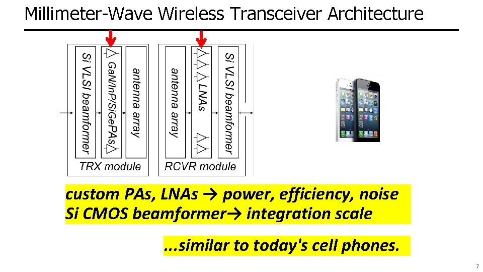
Millimeter-Wave Wireless Transceiver Architecture custom PAs, LNAs → power, efficiency, noise Si CMOS beamformer→ integration scale. . . similar to today's cell phones. 7

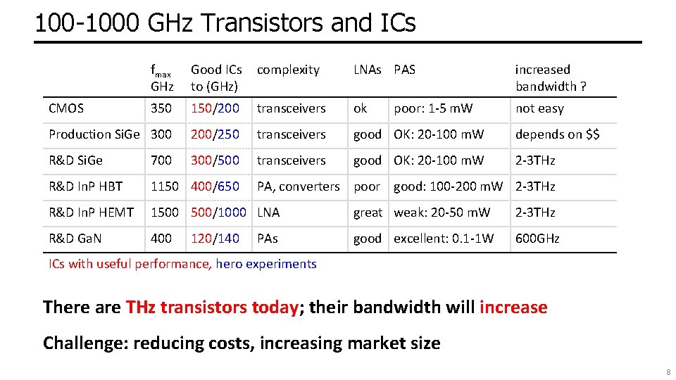
100 -1000 GHz Transistors and ICs fmax GHz Good ICs to (GHz) complexity LNAs PAS increased bandwidth ? 350 150/200 transceivers ok not easy Production Si. Ge 300 200/250 transceivers good OK: 20 -100 m. W depends on $$ R&D Si. Ge 700 300/500 transceivers good OK: 20 -100 m. W 2 -3 THz R&D In. P HBT 1150 400/650 R&D In. P HEMT 1500 500/1000 LNA great weak: 20 -50 m. W 2 -3 THz R&D Ga. N 400 good excellent: 0. 1 -1 W 600 GHz CMOS 120/140 poor: 1 -5 m. W PA, converters poor good: 100 -200 m. W 2 -3 THz PAs ICs with useful performance, hero experiments There are THz transistors today; their bandwidth will increase Challenge: reducing costs, increasing market size 8

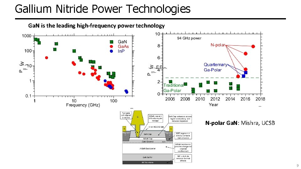
Gallium Nitride Power Technologies Ga. N is the leading high-frequency power technology N-polar Ga. N: Mishra, UCSB 9

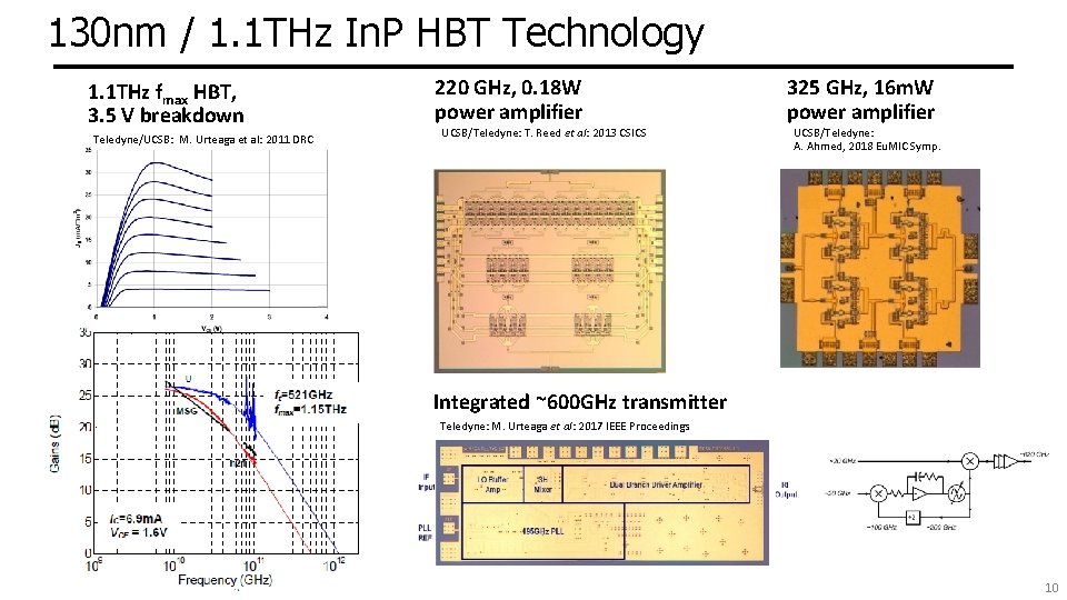
130 nm / 1. 1 THz In. P HBT Technology 1. 1 THz fmax HBT, 3. 5 V breakdown Teledyne/UCSB: M. Urteaga et al: 2011 DRC 220 GHz, 0. 18 W power amplifier UCSB/Teledyne: T. Reed et al: 2013 CSICS 325 GHz, 16 m. W power amplifier UCSB/Teledyne: A. Ahmed, 2018 Eu. MIC Symp. Integrated ~600 GHz transmitter Teledyne: M. Urteaga et al: 2017 IEEE Proceedings 10

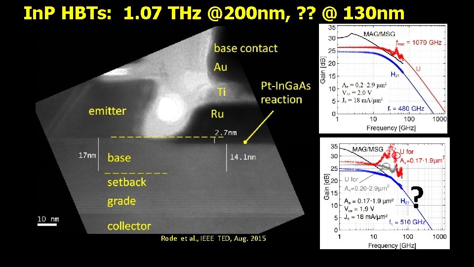
In. P HBTs: 1. 07 THz @200 nm, ? ? @ 130 nm ? Rode et al. , IEEE TED, Aug. 2015 11

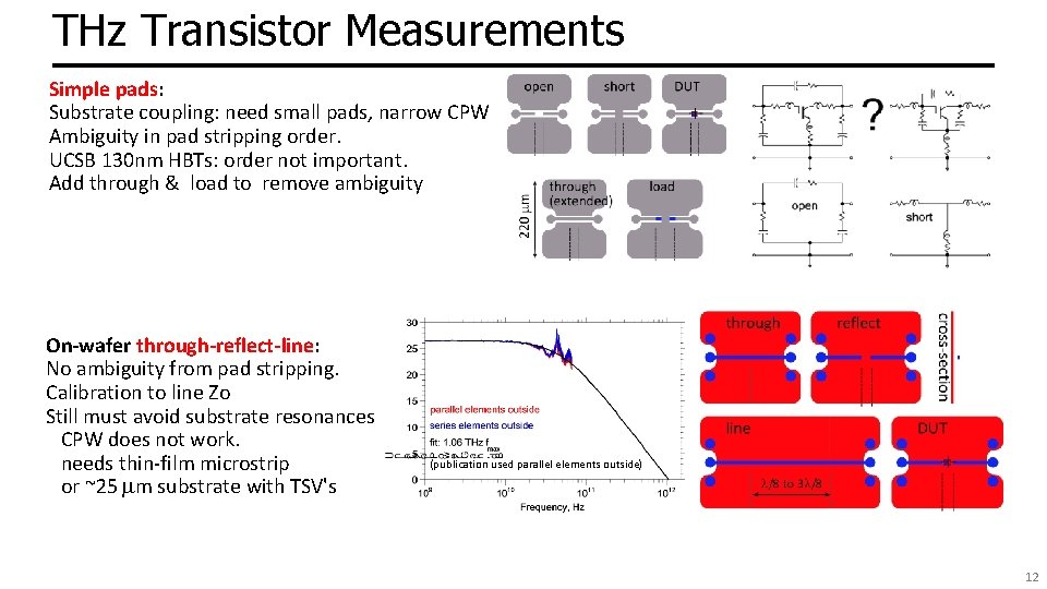
THz Transistor Measurements Simple pads: Substrate coupling: need small pads, narrow CPW Ambiguity in pad stripping order. UCSB 130 nm HBTs: order not important. Add through & load to remove ambiguity On-wafer through-reflect-line: No ambiguity from pad stripping. Calibration to line Zo Still must avoid substrate resonances CPW does not work. needs thin-film microstrip or ~25 mm substrate with TSV's (publication used parallel elements outside) 12

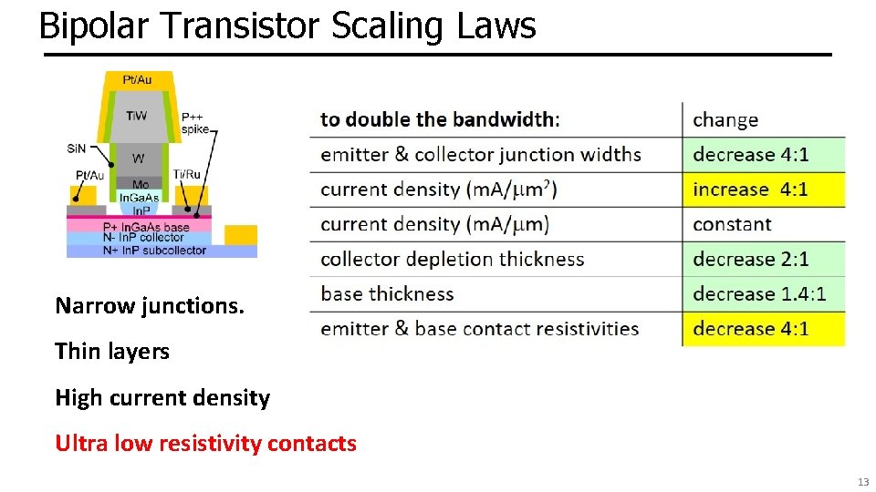
Bipolar Transistor Scaling Laws Narrow junctions. Thin layers High current density Ultra low resistivity contacts 13

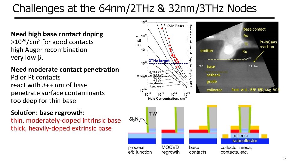
Challenges at the 64 nm/2 THz & 32 nm/3 THz Nodes Need moderate contact penetration Pd or Pt contacts react with 3++ nm of base penetrate surface contaminants too deep for thin base Baraskar et al, Journal of Applied Physics, 2013 Need high base contact doping >1020/cm 3 for good contacts high Auger recombination very low b. Rode et al. , IEEE TED, Aug. 2015 Solution: base regrowth: thin, moderately-doped intrinsic base thick, heavily-doped extrinsic base 14

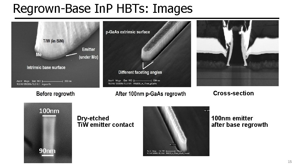
Regrown-Base In. P HBTs: Images Cross-section Dry-etched Ti. W emitter contact 100 nm emitter after base regrowth 15

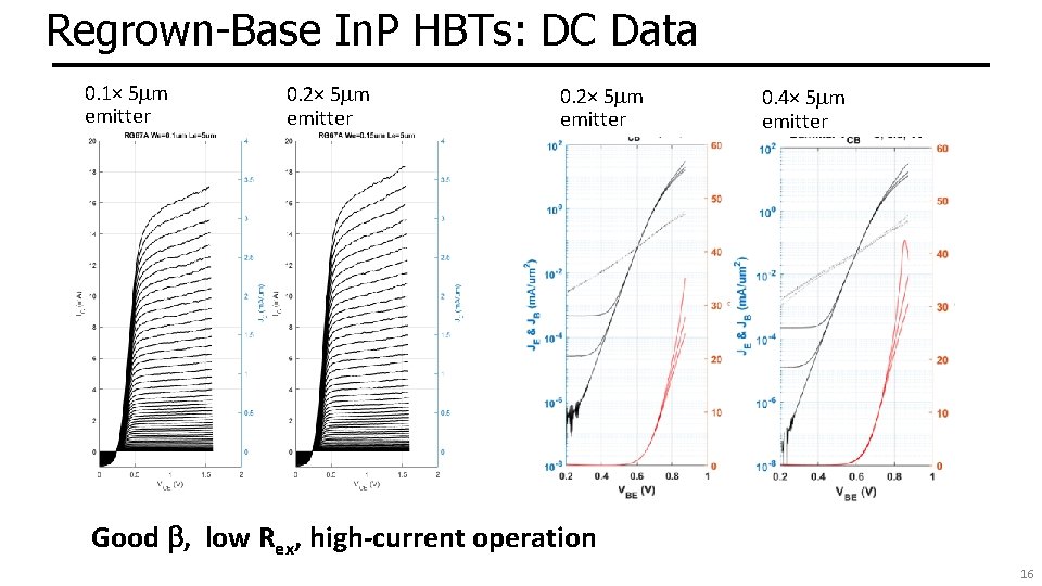
Regrown-Base In. P HBTs: DC Data 0. 1× 5 mm emitter 0. 2× 5 mm emitter 0. 4× 5 mm emitter Good b, low Rex, high-current operation 16

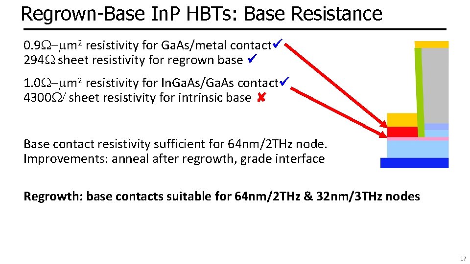
Regrown-Base In. P HBTs: Base Resistance 0. 9 W-mm 2 resistivity for Ga. As/metal contact 294 W sheet resistivity for regrown base 1. 0 W-mm 2 resistivity for In. Ga. As/Ga. As contact 4300 W/ sheet resistivity for intrinsic base ✘ Base contact resistivity sufficient for 64 nm/2 THz node. Improvements: anneal after regrowth, grade interface Regrowth: base contacts suitable for 64 nm/2 THz & 32 nm/3 THz nodes 17

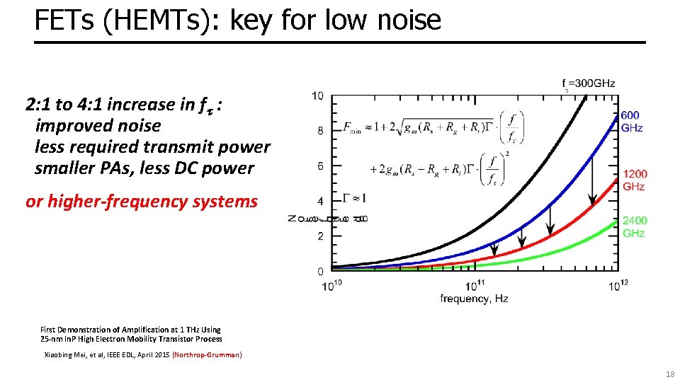
FETs (HEMTs): key for low noise 2: 1 to 4: 1 increase in ft : improved noise less required transmit power smaller PAs, less DC power or higher-frequency systems First Demonstration of Amplification at 1 THz Using 25 -nm In. P High Electron Mobility Transistor Process Xiaobing Mei, et al, IEEE EDL, April 2015 (Northrop-Grumman) 18

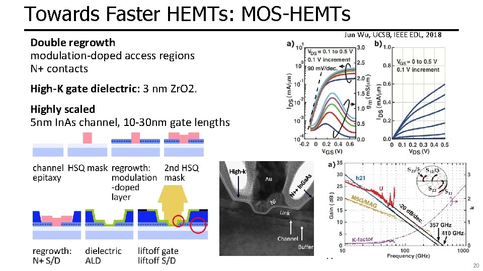
Towards faster HEMTs: MOS-HEMTs 1 st demonstration: Fraunhofer IAF Scaling limit: gate insulator thickness HEMT: In. Al. As barrier: tunneling, thermionic leakage solution: replace In. Al. As with high-K dielectric 2 nm Zr. O 2 (er=25): adequately low leakage Scaling limit: source access resistance HEMT: In. Al. As barrier is under N+ source/drain solution: regrowth, place N+ layer on In. As channel Target ~10 nm node ~0. 3 nm EOT, 3 nm thick channel 1. 2 to 1. 5 THz ft. 19

Towards Faster HEMTs: MOS-HEMTs Double regrowth modulation-doped access regions N+ contacts Jun Wu, UCSB, IEEE EDL, 2018 High-K gate dielectric: 3 nm Zr. O 2. Highly scaled 5 nm In. As channel, 10 -30 nm gate lengths 20

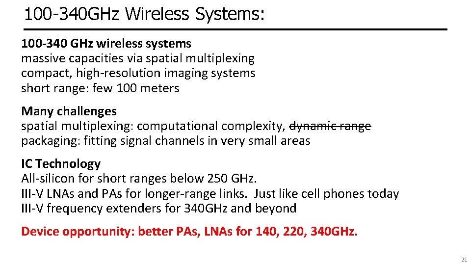
100 -340 GHz Wireless Systems: 100 -340 GHz wireless systems massive capacities via spatial multiplexing compact, high-resolution imaging systems short range: few 100 meters Many challenges spatial multiplexing: computational complexity, dynamic range packaging: fitting signal channels in very small areas IC Technology All-silicon for short ranges below 250 GHz. III-V LNAs and PAs for longer-range links. Just like cell phones today III-V frequency extenders for 340 GHz and beyond Device opportunity: better PAs, LNAs for 140, 220, 340 GHz. 21

In case of questions 22

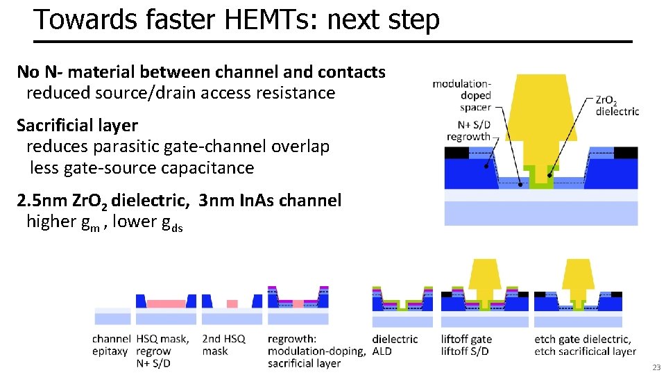
Towards faster HEMTs: next step No N- material between channel and contacts reduced source/drain access resistance Sacrificial layer reduces parasitic gate-channel overlap less gate-source capacitance 2. 5 nm Zr. O 2 dielectric, 3 nm In. As channel higher gm , lower gds 23

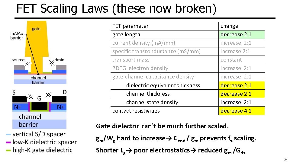
FET Scaling Laws (these now broken) FET parameter gate length current density (m. A/mm) specific transconductance (m. S/mm) transport mass 2 DEG electron density gate-channel capacitance density dielectric equivalent thickness channel state density contact resistivities change decrease 2: 1 increase 2: 1 constant increase 2: 1 decrease 2: 1 increase 2: 1 decrease 4: 1 Gate dielectric can't be much further scaled. gm/Wg hard to increase→ Cend / gm prevents ft scaling. Shorter Lg→ poor electrostatics→ reduced gm /Gds 24

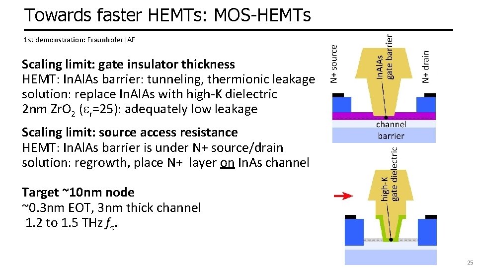
Towards faster HEMTs: MOS-HEMTs 1 st demonstration: Fraunhofer IAF Scaling limit: gate insulator thickness HEMT: In. Al. As barrier: tunneling, thermionic leakage solution: replace In. Al. As with high-K dielectric 2 nm Zr. O 2 (er=25): adequately low leakage Scaling limit: source access resistance HEMT: In. Al. As barrier is under N+ source/drain solution: regrowth, place N+ layer on In. As channel Target ~10 nm node ~0. 3 nm EOT, 3 nm thick channel 1. 2 to 1. 5 THz ft. 25