Transistors Bipolar Junction Transistors First BJTs History The

Transistors

Bipolar Junction Transistors
 The transistor was probably the most important invention of the")
First – BJTs (History) The transistor was probably the most important invention of the 20 th Century, Shockley, Bardeen and Brattain three shared a Nobel Prize in 1955 for invention of transistor. Bardeen and Brattain continued in research (and Bardeen later won another Nobel).

Introduction �Bipolar transistors are one of the main ‘building-blocks’ in electronic systems �They are used in both analogue and digital circuits �The transistor is a three-layer semiconductor device consisting of two nand one p-type layers of material or two pand one n-type layers of material.

BJTs… They incorporate two pn junctions and are sometimes known as bipolar junction transistors or BJTs Here will refer to them simply as bipolar transistors The term bipolar reflects the fact that holes and electrons involve in the current flow.

• The BJT is analogous to a vacuum triode and is comparatively smaller in size. • It is used in amplifier and oscillator circuits, and as a switch in digital circuit. • It has wide applications in computers, satellites and other modern communication system. Department of ECE / EEE 6

Basic models of BJT npn transistor Diode pnp transistor Diode

Recall p-n junction W + P N N P W - + - Vappl < 0 Vappl > 0 Forward bias, + on P, - on N (Shrink W, Vbi) Reverse bias, + on N, - on P (Expand W, Vbi) Allow holes to jump over barrier into N region as minority carriers Remove holes and electrons away from depletion region I I V V

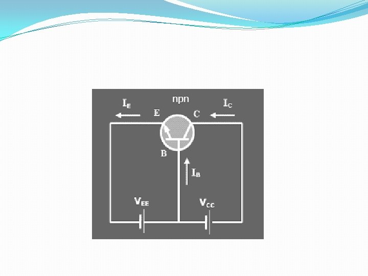
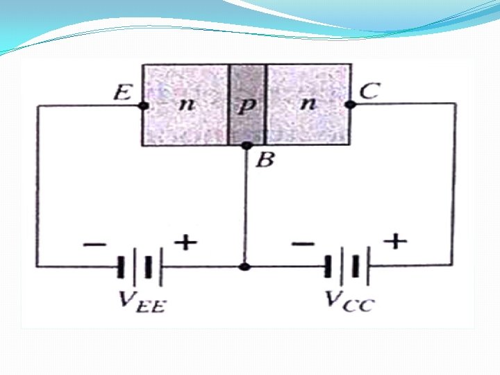
NPN and PNP B E N P B N C NPN E P N P C PNP Department of ECE / EEE 9

• The three portions of the transistor are Emitter, Base and Collector, shown as E, B, and C, respectively. • The arrow on the emitter specifies the direction of current flow when the EB junction is forward biased. • Emitter is heavily doped so that it can inject a large number of charge carriers into the base. • Base is lightly doped and very thin. • It passes most of the injected charge carriers from the emitter into the collector. • Collector is moderately doped. 10

Physical Structure A simplified structure of the npn transistor. 11

Physical Structure A dual of the npn is called pnp type. This is the simplified structure of the pnp transistor. 12

Circuit Symbols for BJTs The emitter is distinguished by the arrowhead. 13

BJTs – Symbol pnp BJT npn BJT

NPN vs PNP NPN and PNP function the same way Power supply polarities are reversed For NPN, positive supply is used NPN has higher frequency response as electrons are the charge carriers. NPN is more widely used

Transistor operation in the active region N-P-N Junction JEB Emitter N RE + - - - - + + - - + Depletion region + - VEE Junction JCB Base P collector N RC Depletion region + - VCC

Transistor operation in the active region N-P-N Junction Holes JEB Electrons Emitter P N RE + - VEE Base Junction JCB - - + + - - + collector N

Transistor operation in the active region N-P-N Junction Holes JEB Electrons Emitter P N RE + - VEE Base Junction JCB - - + + - - + collector N

Transistor operation in the active region N-P-N Junction Holes JEB Electrons Emitter P N RE + - VEE Base Junction JCB - - + + - - + collector N

Transistor operation in the active region N-P-N Junction Holes JEB Electrons Emitter P RE + - VEE Base Junction JCB - - + + - - + collector N

Transistor operation in the active region N-P-N Junction Holes JEB Electrons Emitter P Junction JCB - - + + - - + collector N Base electron current RE + Emitter electron current VEE Base This constitutes the base current IB Thus base current flows due to the Recombination of electrons and holes

Transistor operation in the active region N-P-N Junction Holes JEB Electrons Emitter P Junction JCB - - + + - - + collector N Base electron current RE + Emitter electron current VEE Base - This constitutes the base current IB Thus base current flows due to the Recombination of electrons and holes + VCC

Transistor operation in the active region N-P-N Junction Holes JEB Electrons Emitter P Junction JCB - - + + - - + collector N Collector electron current Base electron current RE + Emitter electron current VEE Base This constitutes the base current IB Thus base current flows due to the Recombination of electrons and holes - + VCC

Transistor operation in the active region N-P-N Junction JEB Junction JCB collector Emitter P N Electron emitted N Electron collected RC RE Collector electron current + Emitter electron current VEE Base This constitutes the base current IB Thus base current flows due to the Recombination of electrons and holes + - VCC

Transistor operation in the active region N-P-N Junction JEB Junction JCB collector Emitter P N Electron emitted RE Direction Conventional Current IE Emitter electron current N Electron collected RC Direction Conventional Current IB + VEE Base + - VCC Direction Conventional Current IC

Transistor operation in the active region N-P-N Junction JEB Junction JCB collector Emitter P N N Electron emitted RE Direction Conventional Current IE Emitter electron current Electron collected RC Direction Conventional Current IB + VEE Base IE = IC + IB + - VCC Direction Conventional Current IC

Transistor operation in the active region P-N-P Junction JEB Junction JCB N P P collector Emitter P N holes emitted holes collected RC RE Collector hole current - + Emitter Hole current VEE Base This constitutes the base current IB Thus base current flows due to the Recombination of electrons and holes - + VCC

Transistor operation in the active region P-N-P Junction JEB Junction JCB N P P collector Emitter P N holes emitted holes collected RC RE conventional current - + Conventional current VEE Base This constitutes the base current IB Thus base current flows due to the Recombination of electrons and holes - + VCC

Transistor operation in the active region P-N-P Junction JEB Junction JCB N P P collector Emitter P N holes emitted holes collected RC RE conventional current - + Conventional current VEE Base IE = IC + IB - + VCC

Transistor current As discussed earlier, the electrons injected from emitter into base constitute the emitter current (IE).

Transistor current As discussed earlier, the electrons injected from emitter into base constitute the emitter current (IE). Out of these electrons very few will combine with the holes in the thin base region to constitute the base current (IB).

Transistor current As discussed earlier, the electrons injected from emitter into base constitute the emitter current (IE). Out of these electrons very few will combine with the holes in the thin base region to constitute the base current (IB). The remaining electrons pass through to the collector region and then to the positive end of Vcc to constitute the collector current (IC).

C Collector Transistor current • Therefore we can write that IE = I C + I B IC IB B Base IE E Emitter

C Collector Transistor current • Therefore we can write that IE = I C + I B IC IB B Base IE E Emitter • Emitter current is always equal to the sum of collector current and base current.

C Collector Transistor current • Therefore we can write that IE = I C + I B IC IB B Base IE E Emitter • Emitter current is always equal to the sum of collector current and base current. • As IB is very small as compared to IE we can assume the collector current to be nearly equal to the emitter current IE ≈ I C

Circuit symbols and conventions of Transistor C C IC N IC JC P B IB IB B JE IE N IE E E N-P-N Transistor

Circuit symbols and conventions of Transistor C C IC N IC JC P B IB IB B JE + VBE N IE - IE E E N-P-N Transistor

Circuit symbols and conventions of Transistor C C IC N IC JC P B IB + IB B JE VCE + VBE N IE - IE E E N-P-N Transistor

Circuit symbols and conventions of Transistor C C IC P IC JC N B IB IB B JE VCE - + VBE IE + P IE E E P-N-P Transistor -

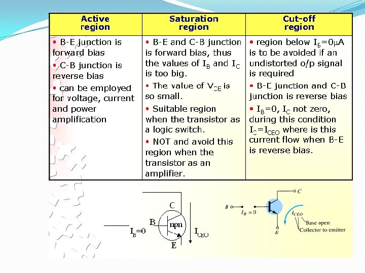
Transistor biasing in different region of operation Sr. Region of No. operation 1 2 3 Base emitter junction Collector base application junction Cutoff region Reverse biased Saturation Forward region biased Reverse biased Forward biased Active region Forward biased Reverse biased Amplifier

Transistor biasing • The following figure shows, usually the emitter-base junction is forward biased and collector-base junction is reverse biased. • Due to the forward bias on the emitter-base junction, an emitter current flows through the base into the collector. • Through the collector-base junction is reverse biased, almost the entire emitter current flows through the collector circuit. Department of ECE / EEE 41

NPN Transistor biasing Department of ECE / EEE 42

PNP Transistor biasing Department of ECE / EEE 43

Transistor Configuration

CB Configuration �This is also called grounded base configuration. In this configuration, emitter is the input terminal, collector is the output terminal and base is the common terminal. �The input is applied between the emitter and base terminals. The output is taken between the collector and base terminals. Department of ECE / EEE 45
 the current amplification factor")
Current relations in CB configuration Current amplification factor ( αdc) the current amplification factor is the ratio of collector current due to the injection of total emitter current IC = IC(INJ) + ICBO ---------------(1)

Common-Emitter Configuration � It is called common-emitter configuration since : - emitter is common or reference to both input and output terminals. - emitter is usually the terminal closest to or at ground potential. � CE configuration is used in amplifier circuits due to the high gain for current and voltage � Two set of characteristics are necessary to describe the behavior for CE ; input (base terminal) and output (collector terminal) parameters.

Proper Biasing common-emitter configuration in active region

IB is microamperes compared to miliamperes of IC. IB will flow when VBE > 0. 7 V for silicon and 0. 3 V for germanium Before this value IB is very small and no IB. Base-emitter junction is forward bias Increasing VCE will reduce IB for different values. Input characteristics for a common-emitter NPN transistor
")
Output characteristics for a common-emitter npn transistor For small VCE (VCE < VCESAT, ) IC increase linearly with increasing of VCE > VCESAT IC does not depend on VCE constant IC IB(u. A) is very small compare to IC (m. A). Small increase in IB cause big increase in IC IB=0 A ICEO occur.
. It is called common-emitter configuration since")
Common – Collector Configuration Also called emitter-follower (EF). It is called common-emitter configuration since both the signal source and the load share the collector terminal as a common connection point. The output voltage is obtained at emitter terminal. The input characteristic of common-collector configuration is similar with common-emitter. configuration. Common-collector circuit configuration is provided with the load resistor connected from emitter to ground. It is used primarily for impedance-matching purpose since it has high input impedance and low output impedance.
 pnp transistor ; (b) npn")
Notation and symbols used with the common-collector configuration: (a) pnp transistor ; (b) npn transistor.
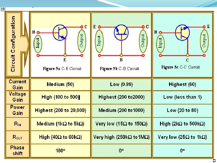

Comparison of CB CE and CC configuration S. No Characteristics CE CB CC 1 Input impedance Medium Low High 2 Output impedance medium High low 3 Current gain High Low High 4 Voltage gain High Unity 5 Power gain High Medium Low 6 Phase reversal Yes No No 7 application Voltage & power amplifiers AF amplifiers Impedance matching 57

DC Biasing and Q point State the purpose of dc biasing circuits. Plot the dc load line given the value of VCC and the total collector-emitter circuit resistance. Describe the Q-point of an amplifier. Describe and analyze the operations of various bias circuits: base-bias circuits voltage-divider bias circuits emitter-bias circuits collector-feedback bias circuits emitter-feedback bias circuits 58

Transistor Operating Point ECE 442 Power Electronics 59
VCE + VCC/RC �Y=m. X +C �Slope= -1/RC �If we plot graph of IC")
�IC=(-1/RC)VCE + VCC/RC �Y=m. X +C �Slope= -1/RC �If we plot graph of IC and VCE for different values of Ib then it will be as below �As equation of straight line and slope depends on load resistance RC so called load line �As it is operated in DC bias so called DC Load Line

DC Load Line VCC/RC VCC ECE 442 Power Electronics 61

A generic dc load line. 62
 Graphical Analysis")
DC Operating Point (Quiescent Point or Q - Point) Graphical Analysis

�We assign three values to IB and observe what happens to IC and VCE. �First, VBB is adjusted to produce an IB of 200µA. �Since IC= DCIB the collector current is 20 m. A, as indicated, and �This Q-point is shown on the graph as Q 1.

�Next, VBB is increased to produce an IB of 300µA and an IC of 30 m. A. �The Q-point for this condition is indicated by Q 2 on the graph.

�Finally, VBB is increased to give an IB of 400µA and an IC of 40 m. A. �Q 3 is the corresponding Q-point on the graph.

Optimum Q-point with amplifier operation 67

Instability in Q Point Due to Temperature Due to gain The operating point of a transistor amplifier shifts mainly with changes in temperature, since the transistor parameters — β, ICO and VBE (where the symbols carry their usual meaning)—are functions of temperature.

Voltage-divider bias characteristics Load line equations: Q-point equations (assume that h. FERE > 10 R 2): 69

�This is the most commonly used arrangement for biasing as it provide good bias stability. �In this arrangement the emitter resistance ‘RE’ provides stabilization. The resistance ‘RE’ cause a voltage drop in a direction so as to reverse bias the emitter junction. �Since the emitter-base junction is to be forward biased, the base voltage is obtained from R 1 -R 2 network. �The net forward bias across the emitter base junction is equal to VB- dc voltage drop across ‘RE’. �The base voltage is set by Vcc and R 1 and R 2. The dc bias circuit is independent of transistor current gain. �In case of amplifier, to avoid the loss of ac signal, a capacitor of large capacitance is connected across RE. The capacitor offers a very small reactance to ac signal and so it passes through the condensor.

Voltage-divider bias characteristics Circuit recognition: The voltage divider in the base circuit. Advantages: The circuit Qpoint values are stable against changes in h. FE. Disadvantages: Requires more components than most other biasing circuits. Applications: Used primarily to bias linear amplifier. 71

Stability of Voltage Divider Bias Circuit The Q-point of voltage divider bias circuit is less dependent on h. FE than that of the base bias (fixed bias). For example, if IE is exactly 10 m. A, the range of h. FE is 100 to 300. Then ICQ hardly changes over the entire range of h. FE. 72

The BJT as a Switch When used as an electronic switch, a transistor normally is operated alternately in cutoff and saturation A transistor is in cutoff when the base-emitter junction is not forward-biased. VCE is approximately equal to VCC When the base-emitter junction is forward-biased and there is enough base current to produce a maximum collector current, the transistor is saturated

The BJT as a Switch

The Transistor as a Switch � The basic element of logic circuits is the transistor switch. A � When the switch is open, i. C = 0 and Vo = VCC. � When the switch is closed, Vo = 0 and � i. C = VCC/RC. � In an electronic circuit, mechanical switches are not used. � The switching action is performed by a transistor with an input voltage switching the circuit. � When Vi = 0, BJT will be in cut-off, i. C = 0, and Vo = VCC (open switch). � When vi is in “high" state, BJT can be in saturation with Vo = VCE = Vsat = 0: 2 V and � IC = (VCC - Vsat)=RC (closed switch). When Rc is replaced with a load, this circuit can switch a load ON or OFF.

A simple Application of a transistor switch

The Transistor as an Amplifier Introduction One of the primary uses of a transistor is to amplify ac signals. This could be an audio signal or perhaps some high frequency radio signal. It has to be able to do this without distorting the original input.

DC and AC Quantities

Amplifier Operation Recall that the purpose of dc biasing was to establish the Q-point for operation. The collector curves and load lines help us to relate the Q-point and its proximity to cutoff and saturation. The Qpoint is best established where the signal variations do not cause the transistor to go into saturation or cutoff. What we are most interested in is the ac signal itself. Since the dc part of the overall signal is filtered out in most cases, we can view a transistor circuit in terms of just its ac component.

Amplifier Operation The boundary between cutoff and saturation is called the linear region. A transistor which operates in the linear region is called a linear amplifier. Note that only the ac component reaches the load because of the capacitive coupling and that the output is 180º out of phase with input.

The ac input voltage produces an ac base current, which results in a much larger ac collector current. The ac collector current produces an ac voltage across RC, thus producing an amplified, but inverted, reproduction of the ac input voltage in the active region of operation

The forward-biased base-emitter junction presents a very low resistance to the ac signal. This internal ac emitter resistance is designated r’eand appears in series with RB. The ac base voltage is Vb = Ie*r’e The ac collector voltage, Vc, equals the ac voltage drop across RC. Vc= Ic * Rc Since Ic ≈ Ie the ac collector voltage is Vc ≈ Ie * Rc

� Vb can be considered the transistor ac input voltage where Vb =Vs - Ib. RB. Vc can be considered the transistor ac output voltage. Since voltage gain is defined as the ratio of the output voltage to the input voltage, the ratio of Vc to Vb is the ac voltage gain, Av, of the transistor. � Av = Vc / Vb � Substituting Ie. RC for Vc and Ier’e for Vb yields � Av = Vc/ Vb ◦ = Ie. RC / Ier’e � The Ie terms cancel; therefore � Av = RC / r’e

Resource Material for the topic Reference Books: Floyd Thomas, Electronic Devices, Prentice Hall, 9 th Edition 2012 Links to Useful Videos: 1. Transistors https: //www. youtube. com/watch? v=0 C 4 uxt. S-tl. Q 2. Fabrication of BJT https: //www. youtube. com/watch? v=_j-YEds. VV 74 Links to Useful Resource material:

Thank You !
- Slides: 85