A 140 GHz TwoChannel CMOS Transmitter using LowCost

- Slides: 26

A 140 GHz Two-Channel CMOS Transmitter using Low-Cost Packaging Technologies Arda Simsek 1, 2, Ahmed S. H. Ahmed 1, Ali A. Farid 1, Utku Soylu 1 and Mark J. W. Rodwell 1 1 University of California Santa Barbara, CA 2 Movandi, Irvine, CA

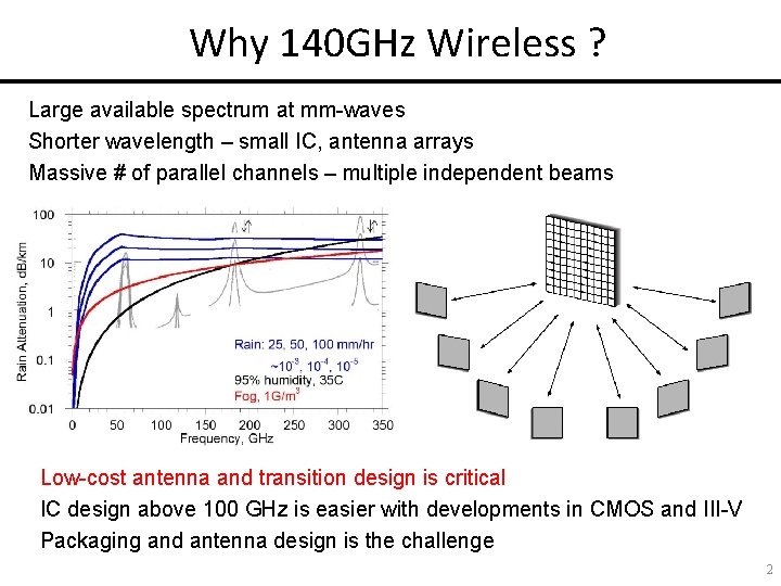
Why 140 GHz Wireless ? Large available spectrum at mm-waves Shorter wavelength – small IC, antenna arrays Massive # of parallel channels – multiple independent beams Low-cost antenna and transition design is critical IC design above 100 GHz is easier with developments in CMOS and III-V Packaging and antenna design is the challenge 2

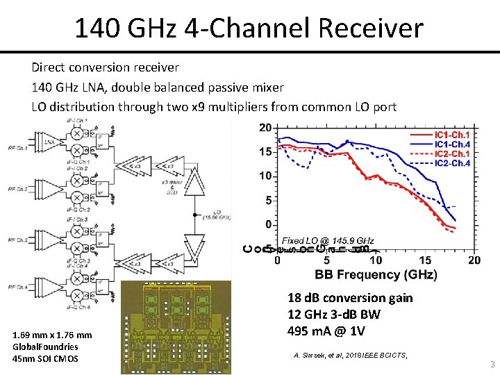
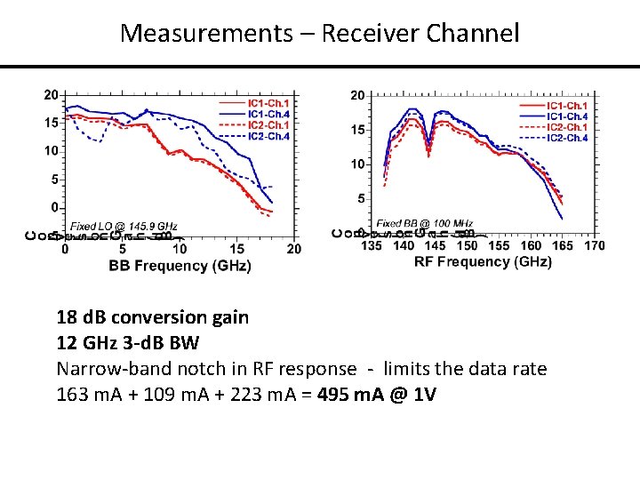
140 GHz 4 -Channel Receiver Direct conversion receiver 140 GHz LNA, double balanced passive mixer LO distribution through two x 9 multipliers from common LO port 1. 69 mm x 1. 76 mm Global. Foundries 45 nm SOI CMOS 18 d. B conversion gain 12 GHz 3 -d. B BW 495 m. A @ 1 V A. Simsek, et al, 2018 IEEE BCICTS, 3

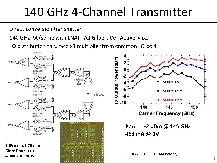
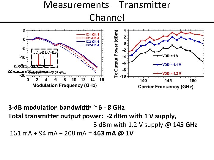
140 GHz 4 -Channel Transmitter Direct conversion transmitter 140 GHz PA (same with LNA), I/Q Gilbert Cell Active Mixer LO distribution thru two x 9 multiplier from common LO port Pout = -2 d. Bm @ 145 GHz 463 m. A @ 1 V 1. 69 mm x 1. 76 mm Global. Foundries 45 nm SOI CMOS A. Simsek, et al, 2018 IEEE BCICTS, 4

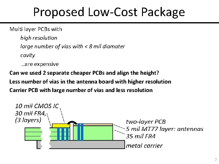
Proposed Low-Cost Package Multi layer PCBs with high resolution large number of vias with < 8 mil diamater cavity …are expensive Can we used 2 separate cheaper PCBs and align the height? Less number of vias in the antenna board with higher resolution Carrier PCB with large number of vias and less resolution 5

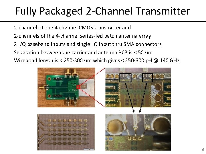
Fully Packaged 2 -Channel Transmitter 2 -channel of one 4 -channel CMOS transmitter and 2 -channels of the 4 -channel series-fed patch antenna array 2 I/Q baseband inputs and single LO input thru SMA connectors Separation between the carrier and antenna PCB is < 50 um Wirebond length is < 250 -300 um which gives < 250 -300 p. H @ 140 GHz 6

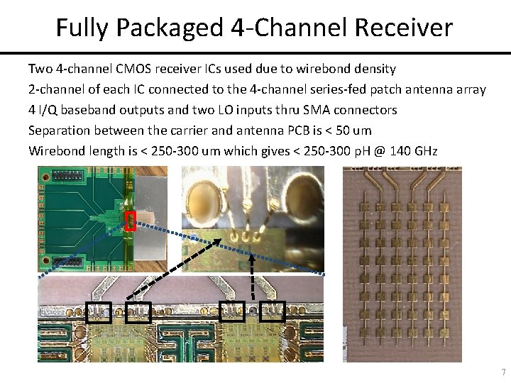
Fully Packaged 4 -Channel Receiver Two 4 -channel CMOS receiver ICs used due to wirebond density 2 -channel of each IC connected to the 4 -channel series-fed patch antenna array 4 I/Q baseband outputs and two LO inputs thru SMA connectors Separation between the carrier and antenna PCB is < 50 um Wirebond length is < 250 -300 um which gives < 250 -300 p. H @ 140 GHz 7

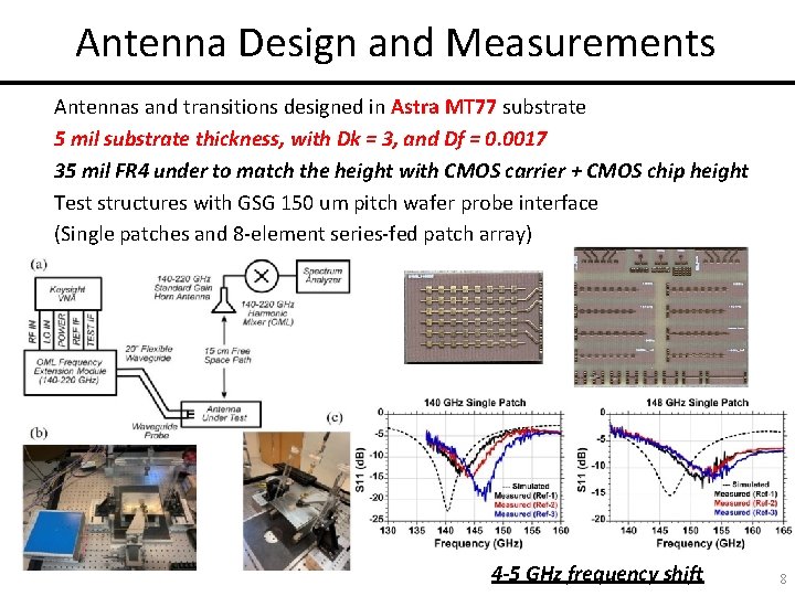
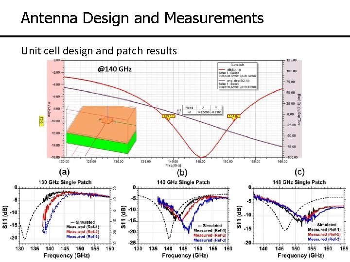
Antenna Design and Measurements Antennas and transitions designed in Astra MT 77 substrate 5 mil substrate thickness, with Dk = 3, and Df = 0. 0017 35 mil FR 4 under to match the height with CMOS carrier + CMOS chip height Test structures with GSG 150 um pitch wafer probe interface (Single patches and 8 -element series-fed patch array) 4 -5 GHz frequency shift 8

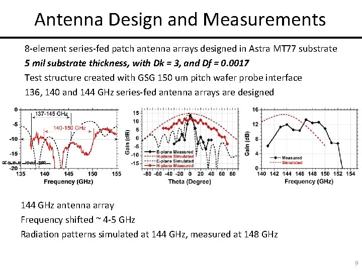
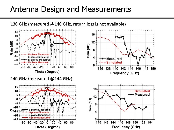
Antenna Design and Measurements 8 -element series-fed patch antenna arrays designed in Astra MT 77 substrate 5 mil substrate thickness, with Dk = 3, and Df = 0. 0017 Test structure created with GSG 150 um pitch wafer probe interface 136, 140 and 144 GHz series-fed antenna arrays are designed 144 GHz antenna array Frequency shifted ~ 4 -5 GHz Radiation patterns simulated at 144 GHz, measured at 148 GHz 9

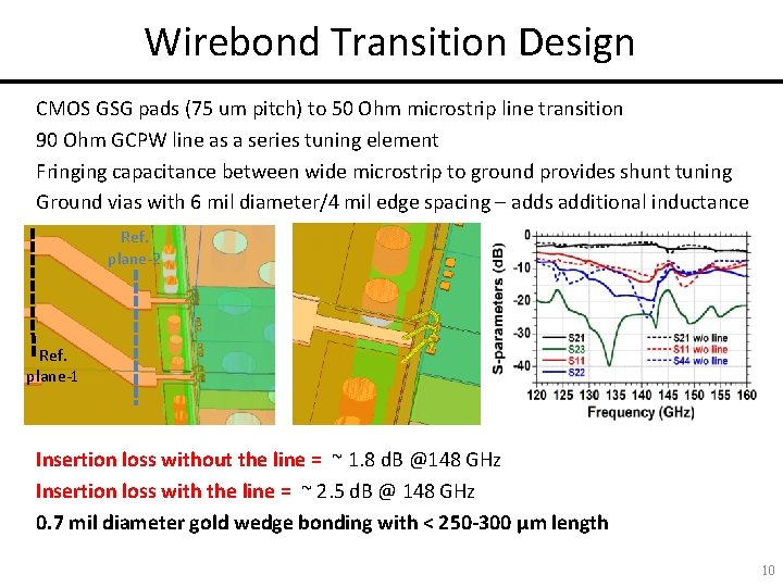
Wirebond Transition Design CMOS GSG pads (75 um pitch) to 50 Ohm microstrip line transition 90 Ohm GCPW line as a series tuning element Fringing capacitance between wide microstrip to ground provides shunt tuning Ground vias with 6 mil diameter/4 mil edge spacing – adds additional inductance Ref. plane-2 Ref. plane-1 Insertion loss without the line = ~ 1. 8 d. B @148 GHz Insertion loss with the line = ~ 2. 5 d. B @ 148 GHz 0. 7 mil diameter gold wedge bonding with < 250 -300 μm length 10

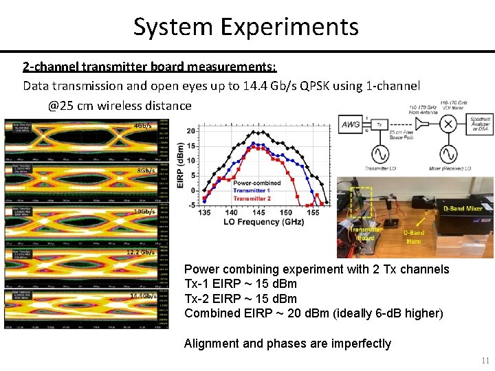
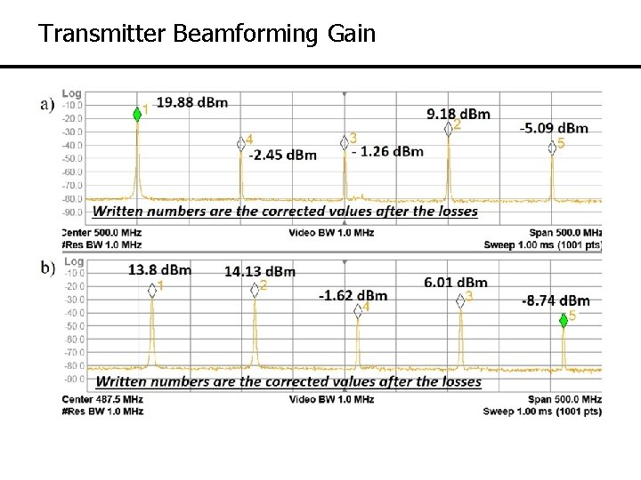
System Experiments 2 -channel transmitter board measurements: Data transmission and open eyes up to 14. 4 Gb/s QPSK using 1 -channel @25 cm wireless distance Power combining experiment with 2 Tx channels Tx-1 EIRP ~ 15 d. Bm Tx-2 EIRP ~ 15 d. Bm Combined EIRP ~ 20 d. Bm (ideally 6 -d. B higher) Alignment and phases are imperfectly 11

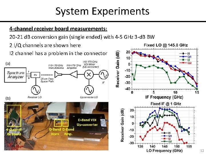
System Experiments 4 -channel receiver board measurements: 20 -21 d. B conversion gain (single ended) with 4 -5 GHz 3 -d. B BW 2 I/Q channels are shown here I 2 channel has a problem in the connector 12

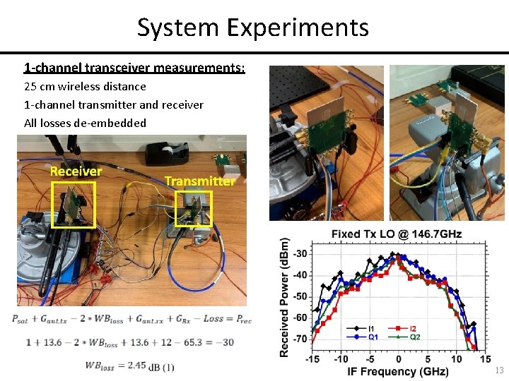
System Experiments 1 -channel transceiver measurements: 25 cm wireless distance 1 -channel transmitter and receiver All losses de-embedded 13

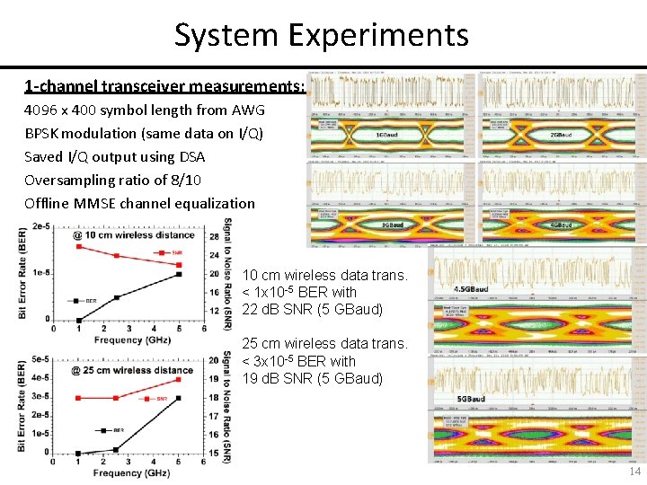
System Experiments 1 -channel transceiver measurements: 4096 x 400 symbol length from AWG BPSK modulation (same data on I/Q) Saved I/Q output using DSA Oversampling ratio of 8/10 Offline MMSE channel equalization 10 cm wireless data trans. < 1 x 10 -5 BER with 22 d. B SNR (5 GBaud) 25 cm wireless data trans. < 3 x 10 -5 BER with 19 d. B SNR (5 GBaud) 14

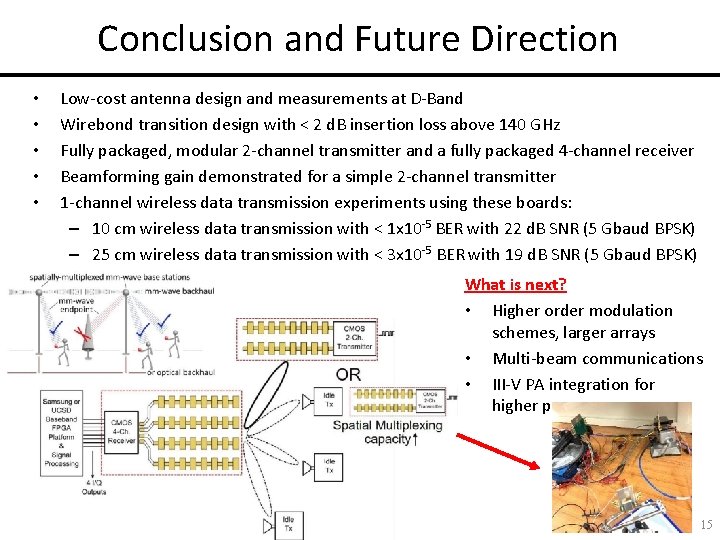
Conclusion and Future Direction • • • Low-cost antenna design and measurements at D-Band Wirebond transition design with < 2 d. B insertion loss above 140 GHz Fully packaged, modular 2 -channel transmitter and a fully packaged 4 -channel receiver Beamforming gain demonstrated for a simple 2 -channel transmitter 1 -channel wireless data transmission experiments using these boards: – 10 cm wireless data transmission with < 1 x 10 -5 BER with 22 d. B SNR (5 Gbaud BPSK) – 25 cm wireless data transmission with < 3 x 10 -5 BER with 19 d. B SNR (5 Gbaud BPSK) What is next? • Higher order modulation schemes, larger arrays • Multi-beam communications • III-V PA integration for higher power 15

Acknowledgments • National Science Foundation (NSF) Giga. Nets program, Contract NO. CNS-1518812 • Global Foundries for the 45 nm CMOS SOI chip fabrication • Advotech for the assembly • Navneet Sharma, Hamidreza Memerzadeh, Nikolaus Klammer and Gary Xu at Samsung Research America for valuable suggestions and the measurement equipment. • Prof. James F. Buckwalter for valuable comments. 16

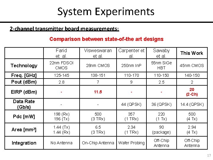
System Experiments 2 -channel transmitter board measurements: Comparison between state-of-the art designs Farid et al. Visweswaran et al. Carpenter et al. Sawaby et al. This Work 22 nm FDSOI CMOS 28 nm CMOS 250 nm In. P 55 nm Si. Ge HBT 45 nm CMOS Freq. [GHz] Pout (d. Bm) 125 -145 138 -151 110 -170 110 -150 140 -150 2. 8 7 9 2. 5 2 EIRP (d. Bm) - 11. 5 - - 20 (2 -Ch) Data Rate (Gb/s) - - 44 (QPSK) 36 (QPSK) 14. 4 (QPSK) Pdc [m. W] 198 (Rx) 196 (Tx) 500 (3 TRx) 357 (1 TRx) 220 (1 Tx) 500 (4 Tx) Area [mm 2] 1. 44 (Tx) 1. 44 (Rx) 6. 5 (3 TRx) 2. 34 (1 TRx) 90 (package) 2. 94 (4 Tx) Integration No Antenna On-Chip Antenna Wafer Probing Off-Chip Antenna Technology 17

Back-up Slides

Antenna Design and Measurements Unit cell design and patch results

Antenna Design and Measurements 136 GHz (measured @140 GHz, return loss is not available) 140 GHz (measured @144 GHz)

Transmitter Beamforming Gain

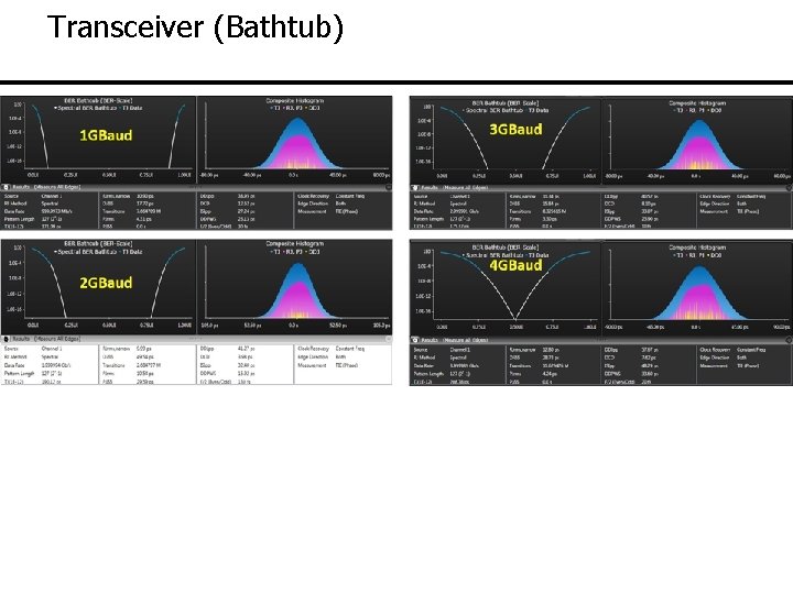
Transceiver (Bathtub)

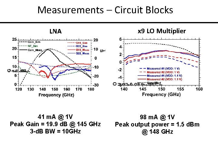
Measurements – Circuit Blocks LNA 41 m. A @ 1 V Peak Gain = 19. 9 d. B @ 145 GHz 3 -d. B BW = 10 GHz x 9 LO Multiplier 98 m. A @ 1 V Peak output power = 1. 5 d. Bm @ 148 GHz

Measurements – Receiver Channel 18 d. B conversion gain 12 GHz 3 -d. B BW Narrow-band notch in RF response - limits the data rate 163 m. A + 109 m. A + 223 m. A = 495 m. A @ 1 V

Measurements – Transmitter Channel LO-BB LO+BB LO 3 -d. B modulation bandwidth ~ 6 - 8 GHz Total transmitter output power: -2 d. Bm with 1 V supply, 3 d. Bm with 1. 2 V supply @ 145 GHz 161 m. A + 94 m. A + 208 m. A = 463 m. A @ 1 V

Outline • Motivation • 140 GHz Transceiver in 45 nm CMOS SOI • Proposed Low-Cost Package – 2 -Channel Transmitter – 4 -Channel Receiver • Wirebond Transition Design • 140 GHz Antenna Design and Measurements • System Experiments and Results • Conclusion and Future Direction 26