Transistors Introduction Transistors are three terminal devices that

- Slides: 21

Transistors

Introduction ® Transistors are three terminal devices that replaced vacuum tubes. ® They are solid state devices that are used for… Amplification ® Switching ® Detecting Light ® ® The three terminals are ® Emitter, Base, Collector ® Source, Gate, Drain the… (BJT) (FET)

The BJT ® Bipolar Junction Transistors are made with n-type and p-type semiconductors. ® There ® Circuit are two types: npn and pnp. Symbols ® Transistor Analogy

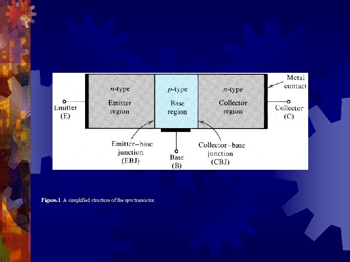
Figure. 1 A simplified structure of the npn transistor.

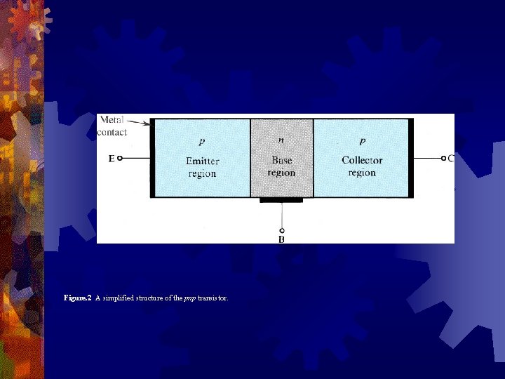
Figure. 2 A simplified structure of the pnp transistor.

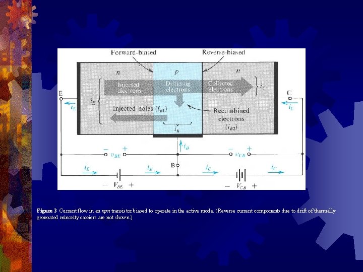
Figure 3 Current flow in an npn transistor biased to operate in the active mode. (Reverse current components due to drift of thermally generated minority carriers are not shown. )

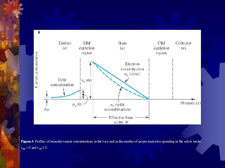
Figure. 4 Profiles of minority-carrier concentrations in the base and in the emitter of an npn transistor operating in the active mode: v. BE > 0 and v. CB ³ 0.

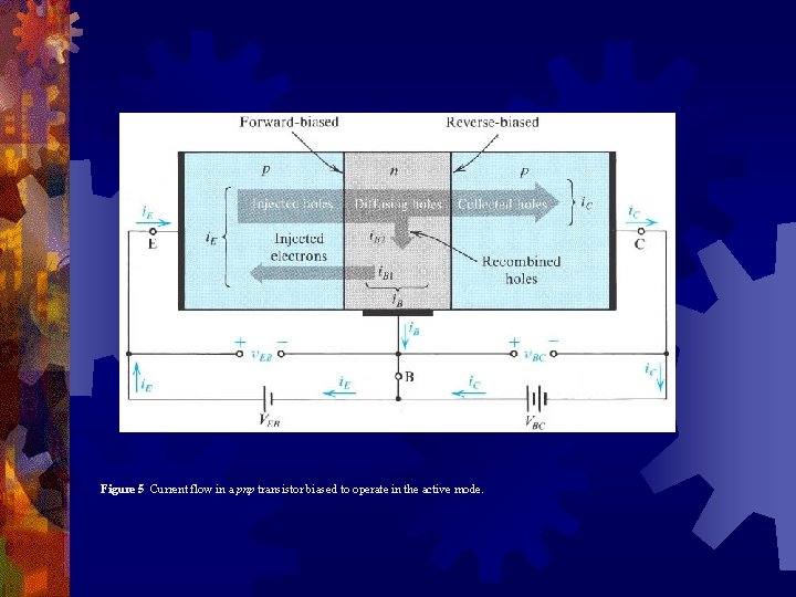
Figure 5 Current flow in a pnp transistor biased to operate in the active mode.

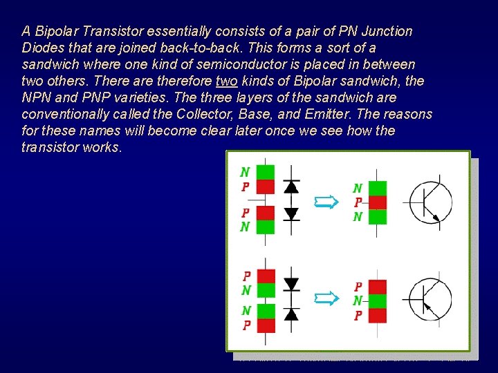
A Bipolar Transistor essentially consists of a pair of PN Junction Diodes that are joined back-to-back. This forms a sort of a sandwich where one kind of semiconductor is placed in between two others. There are therefore two kinds of Bipolar sandwich, the NPN and PNP varieties. The three layers of the sandwich are conventionally called the Collector, Base, and Emitter. The reasons for these names will become clear later once we see how the transistor works.

Some of the basic properties exhibited by a Bipolar Transistor are immediately recognizable as being diode-like. However, when the 'filling' of the sandwich is fairly thin some interesting effects become possible that allow us to use the Transistor as an amplifier or a switch. To see how the Bipolar Transistor works we can concentrate on the NPN variety.

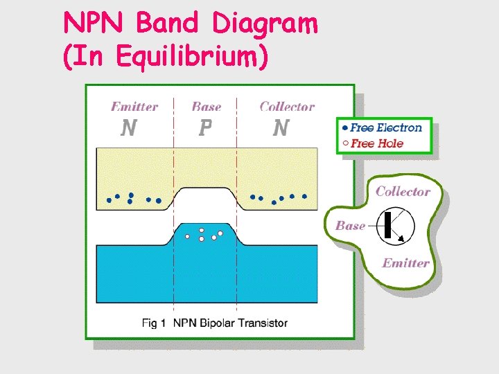
NPN Band Diagram (In Equilibrium)

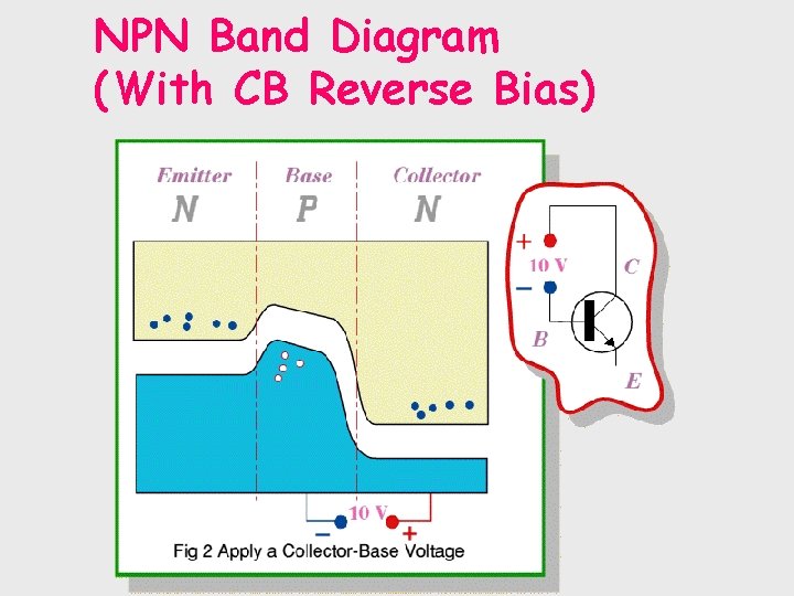
NPN Band Diagram (With CB Reverse Bias)

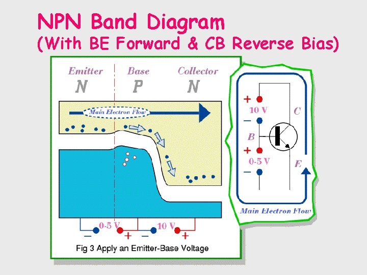
NPN Band Diagram (With BE Forward & CB Reverse Bias)

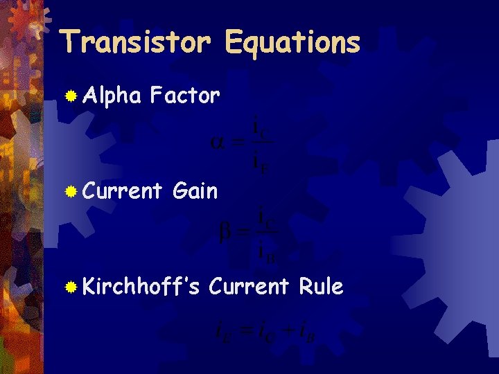
Transistor Equations ® Alpha Factor ® Current Gain ® Kirchhoff’s Current Rule

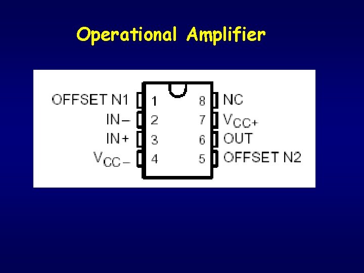
What are the primary uses of transistors? 1. Switching (Logic Gates) 2. Amplification (Op. Amps)

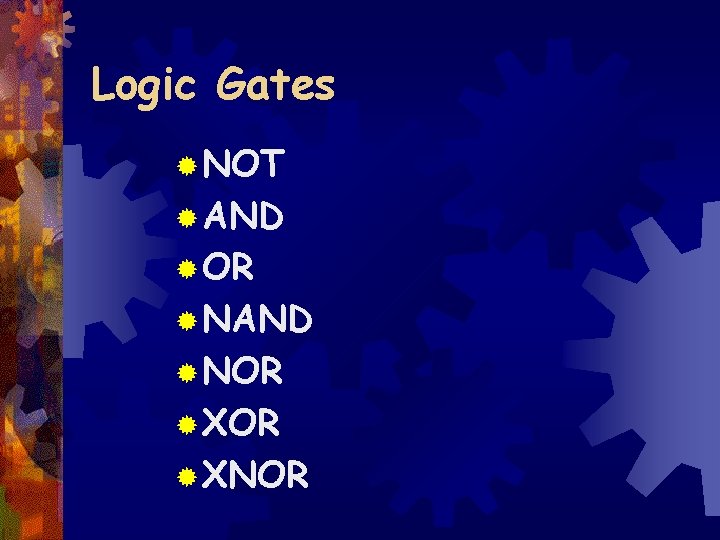
Logic Gates ® NOT ® AND ® OR ® NAND ® NOR ® XNOR

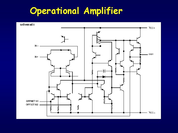
Operational Amplifier

Operational Amplifier

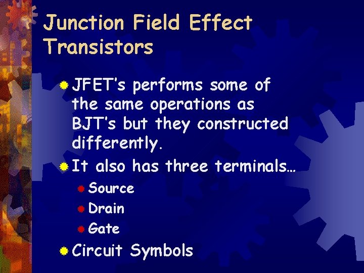
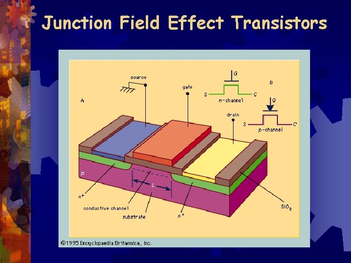
Junction Field Effect Transistors ® JFET’s performs some of the same operations as BJT’s but they constructed differently. ® It also has three terminals… ® Source ® Drain ® Gate ® Circuit Symbols

Junction Field Effect Transistors

Transistor Configurations ® Common Emitter ® Common Collector ® Common Base ® Emitter Follower ® Darlington Configuration ® Transistor Switch