1 3 rd Annual SFR Workshop Review May

- Slides: 51

1 3 rd Annual SFR Workshop & Review, May 24, 2001 8: 30 – 9: 00 – 9: 45 – 10: 30 – 10: 45 – 12: 00 – 1: 45 – 2: 30 – 2: 40 – 3: 30 – 4: 30 – 9: 00 9: 45 10: 30 10: 45 12: 00 1: 45 2: 30 2: 45 4: 30 5: 30 5/24/2001 Research and Educational Objectives / Spanos CMP / Doyle, Dornfeld, Talbot, Spanos Plasma & Diffusion / Graves, Lieberman, Cheung, Haller break Poster Session / Education, CMP, Plasma, Diffusion lunch Lithography / Spanos, Neureuther, Bokor Sensors & Controls /Aydil, Poolla, Smith, Dunn, Cheung, Spanos Break Poster Session / all subjects Steering Committee Meeting in room 373 Soda Feedback Session

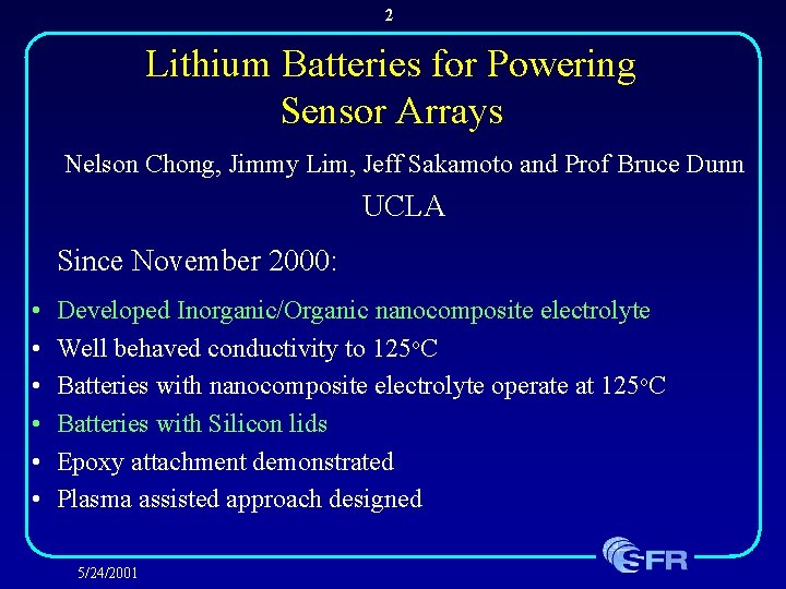
2 Lithium Batteries for Powering Sensor Arrays Nelson Chong, Jimmy Lim, Jeff Sakamoto and Prof Bruce Dunn UCLA Since November 2000: • • • Developed Inorganic/Organic nanocomposite electrolyte Well behaved conductivity to 125 o. C Batteries with nanocomposite electrolyte operate at 125 o. C Batteries with Silicon lids Epoxy attachment demonstrated Plasma assisted approach designed 5/24/2001

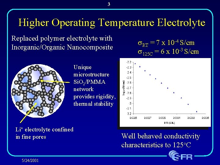
3 Higher Operating Temperature Electrolyte Replaced polymer electrolyte with Inorganic/Organic Nanocomposite s. RT = 7 x 10 -4 S/cm s 125 C = 6 x 10 -3 S/cm Unique microstructure Si. O 2/PMMA network provides rigidity, thermal stability Li+ electrolyte confined in fine pores 5/24/2001 Well behaved conductivity characteristics to 125 o. C

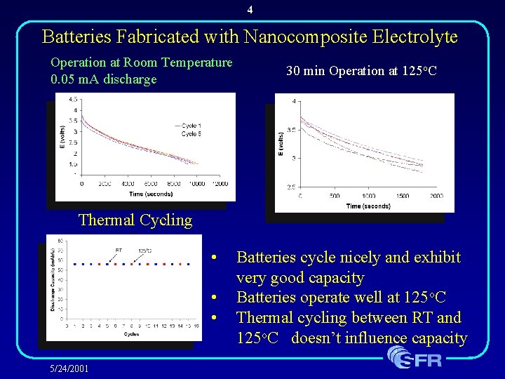
4 Batteries Fabricated with Nanocomposite Electrolyte Operation at Room Temperature 0. 05 m. A discharge 30 min Operation at 125 o. C Thermal Cycling • • • 5/24/2001 Batteries cycle nicely and exhibit very good capacity Batteries operate well at 125 o. C Thermal cycling between RT and 125 o. C doesn’t influence capacity

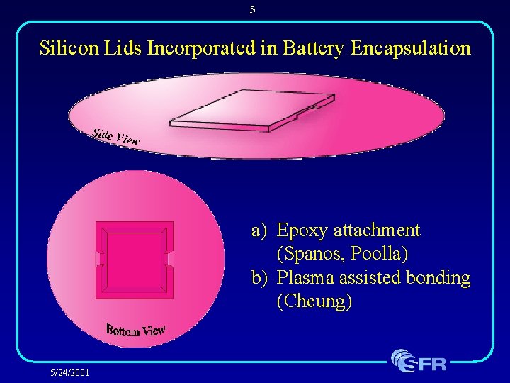
5 Silicon Lids Incorporated in Battery Encapsulation a) Epoxy attachment (Spanos, Poolla) b) Plasma assisted bonding (Cheung) 5/24/2001

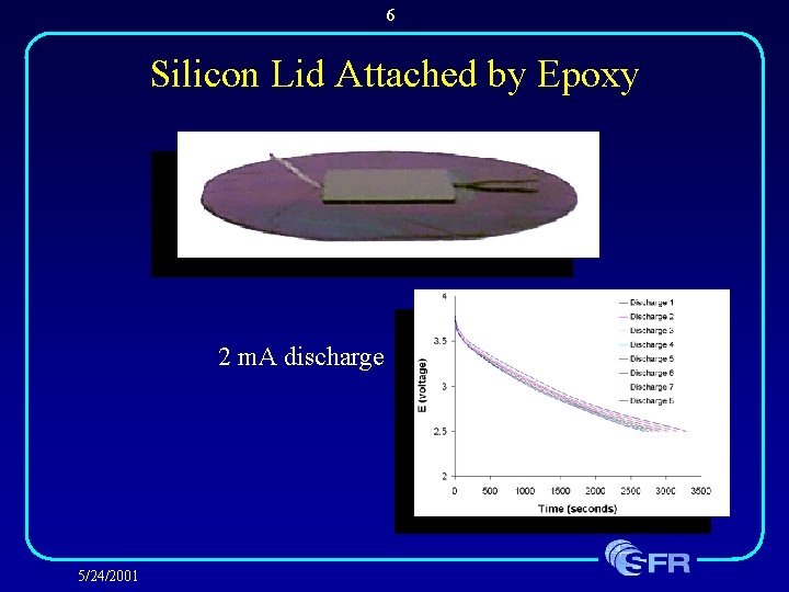
6 Silicon Lid Attached by Epoxy 2 m. A discharge 5/24/2001

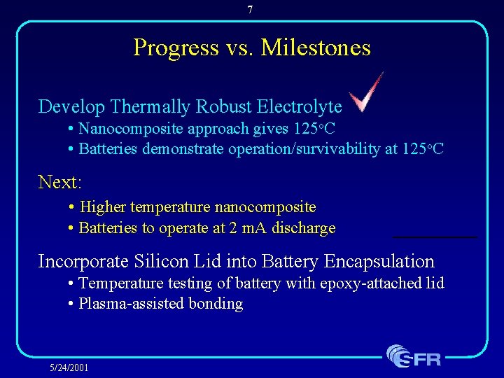
7 Progress vs. Milestones Develop Thermally Robust Electrolyte • Nanocomposite approach gives 125 o. C • Batteries demonstrate operation/survivability at 125 o. C Next: • Higher temperature nanocomposite • Batteries to operate at 2 m. A discharge Incorporate Silicon Lid into Battery Encapsulation • Temperature testing of battery with epoxy-attached lid • Plasma-assisted bonding 5/24/2001

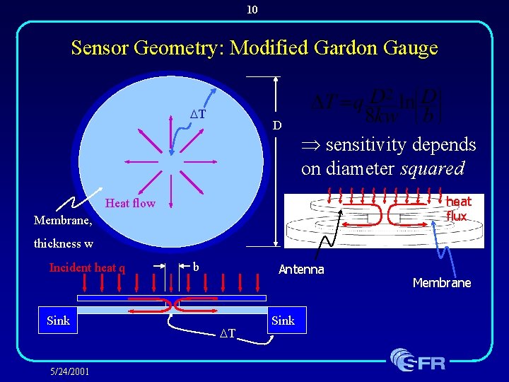
8 Spatially Resolved Heat Flux Sensor on a Silicon Wafer for Plasma Etch Processes Mason Freed, Costas Spanos, Kameshwar Poolla Berkeley, CA 2001 GOAL: Design, build, and test an array of heat flux sensors on a silicon wafer, with external electronics. 5/24/2001

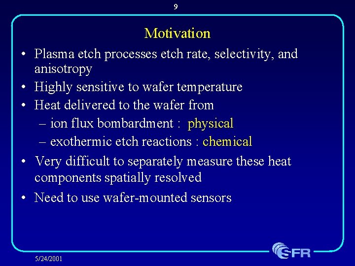
9 Motivation • Plasma etch processes etch rate, selectivity, and anisotropy • Highly sensitive to wafer temperature • Heat delivered to the wafer from – ion flux bombardment : physical – exothermic etch reactions : chemical • Very difficult to separately measure these heat components spatially resolved • Need to use wafer-mounted sensors 5/24/2001

10 Sensor Geometry: Modified Gardon Gauge T D sensitivity depends on diameter squared heat flux Heat flow Membrane, thickness w Incident heat q Sink 5/24/2001 b Antenna T Sink Membrane

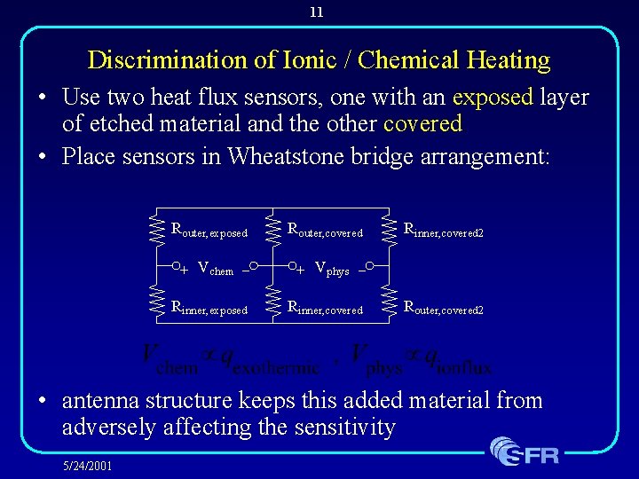
11 Discrimination of Ionic / Chemical Heating • Use two heat flux sensors, one with an exposed layer of etched material and the other covered • Place sensors in Wheatstone bridge arrangement: Router, exposed Router, covered + Vchem – + Vphys – Rinner, exposed Rinner, covered 2 Router, covered 2 • antenna structure keeps this added material from adversely affecting the sensitivity 5/24/2001

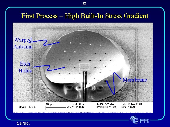
12 First Process – High Built-In Stress Gradient Warped Antenna Etch Holes Membrane 5/24/2001

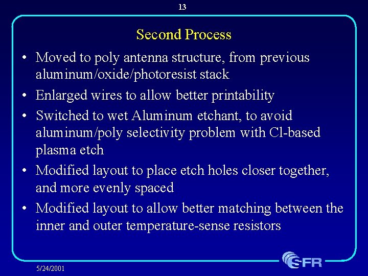
13 Second Process • Moved to poly antenna structure, from previous aluminum/oxide/photoresist stack • Enlarged wires to allow better printability • Switched to wet Aluminum etchant, to avoid aluminum/poly selectivity problem with Cl-based plasma etch • Modified layout to place etch holes closer together, and more evenly spaced • Modified layout to allow better matching between the inner and outer temperature-sense resistors 5/24/2001

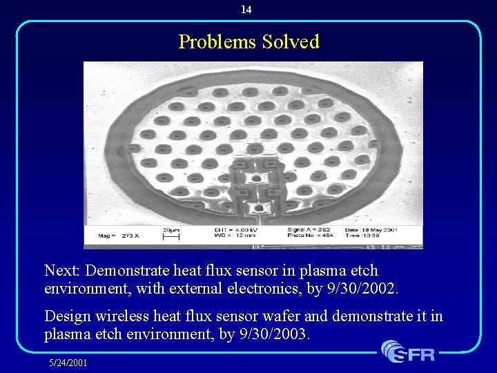
14 Problems Solved Next: Demonstrate heat flux sensor in plasma etch environment, with external electronics, by 9/30/2002. Design wireless heat flux sensor wafer and demonstrate it in plasma etch environment, by 9/30/2003. 5/24/2001

15 Electrical Impedance Tomography based Metrology Michiel Krüger, K. Poolla, C. Spanos Berkeley, CA 2001 GOAL: to demonstrate the feasibility of off-line metrology based on electrical impedance tomography by 9/30/2001. 5/24/2001

16 Problem formulation and motivation • Obtain spatial and temporal information of wafer state during processing, ex: – Etch rate/uniformity across wafer – Plasma induced potential on wafer surface – Wafer surface temperature • Motivation: – Spatial and temporal wafer state information provide useful information about process uniformity. – This information can be used for: • Diagnostics (drifts, detection of process instabilities) • Design (electrode configuration in plasma tools) • Control (to reduce process variability) 5/24/2001

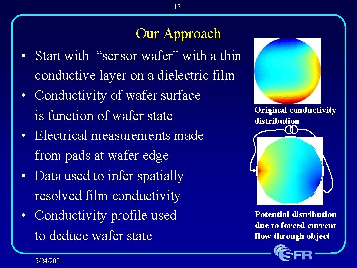
17 Our Approach • Start with “sensor wafer” with a thin conductive layer on a dielectric film • Conductivity of wafer surface is function of wafer state • Electrical measurements made from pads at wafer edge • Data used to infer spatially resolved film conductivity • Conductivity profile used to deduce wafer state 5/24/2001 Original conductivity distribution Potential distribution due to forced current flow through object

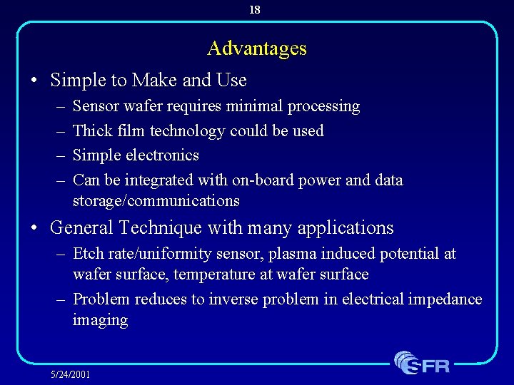
18 Advantages • Simple to Make and Use – – Sensor wafer requires minimal processing Thick film technology could be used Simple electronics Can be integrated with on-board power and data storage/communications • General Technique with many applications – Etch rate/uniformity sensor, plasma induced potential at wafer surface, temperature at wafer surface – Problem reduces to inverse problem in electrical impedance imaging 5/24/2001

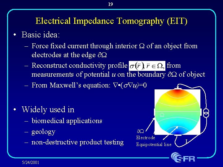
19 Electrical Impedance Tomography (EIT) • Basic idea: – Force fixed current through interior W of an object from electrodes at the edge W – Reconstruct conductivity profile from measurements of potential u on the boundary W of object – From Maxwell’s equation: • (s u)=0 • Widely used in – biomedical applications – geology – non-destructive product testing 5/24/2001 W W Electrode Equipotential line I

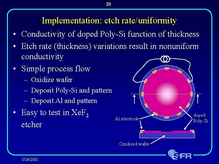
20 Implementation: etch rate/uniformity • Conductivity of doped Poly-Si function of thickness • Etch rate (thickness) variations result in nonuniform conductivity • Simple process flow – Oxidize wafer – Deposit Poly-Si and pattern – Deposit Al and pattern • Easy to test in Xe. F 2 etcher Al electrode Oxidized wafer 5/24/2001 doped Poly-Si

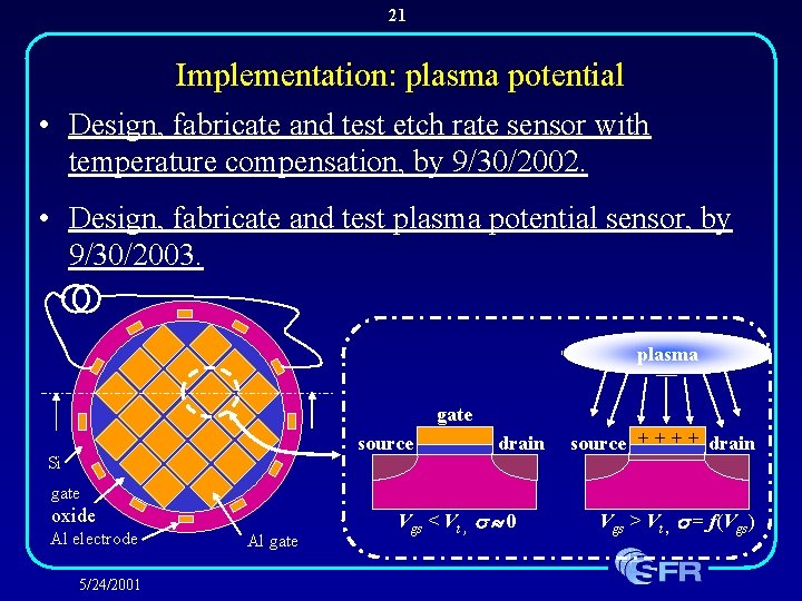
21 Implementation: plasma potential • Design, fabricate and test etch rate sensor with temperature compensation, by 9/30/2002. • Design, fabricate and test plasma potential sensor, by 9/30/2003. plasma gate source Si drain source + + drain gate oxide Al electrode 5/24/2001 Al gate Vgs < Vt , 0 Vgs > Vt , = f(Vgs)

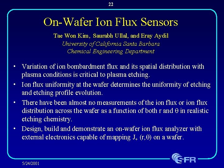
22 On-Wafer Ion Flux Sensors Tae Won Kim, Saurabh Ullal, and Eray Aydil University of California Santa Barbara Chemical Engineering Department • Variation of ion bombardment flux and its spatial distribution with plasma conditions is critical to plasma etching. • Ion flux uniformity at the wafer determines the uniformity of etching and etching profile evolution. • There have been almost no measurements of the ion flux or ion flux distribution across the wafer as a function of both r and q in realistic etching chemistry. • Design, build and demonstrate an on-wafer ion flux analyzer with external electronics capable of mapping J+ (r, q) on a wafer. 5/24/2001

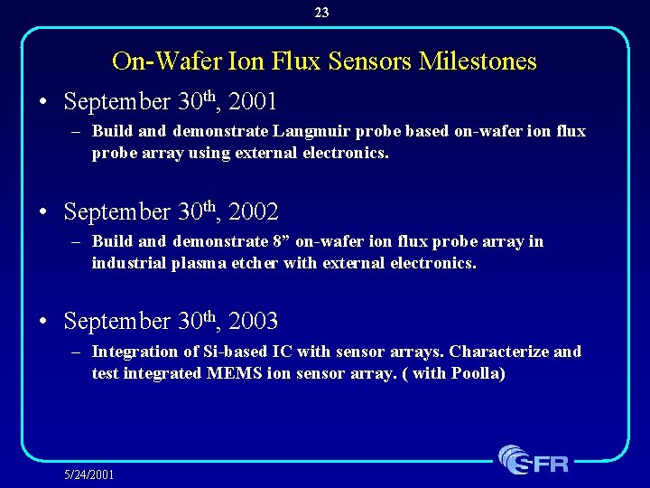
23 On-Wafer Ion Flux Sensors Milestones • September 30 th, 2001 – Build and demonstrate Langmuir probe based on-wafer ion flux probe array using external electronics. • September 30 th, 2002 – Build and demonstrate 8” on-wafer ion flux probe array in industrial plasma etcher with external electronics. • September 30 th, 2003 – Integration of Si-based IC with sensor arrays. Characterize and test integrated MEMS ion sensor array. ( with Poolla) 5/24/2001

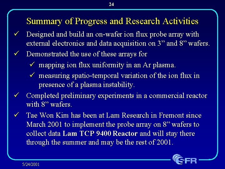
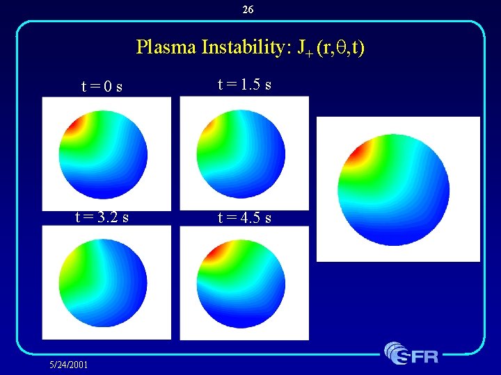
24 Summary of Progress and Research Activities ü Designed and build an on-wafer ion flux probe array with external electronics and data acquisition on 3” and 8” wafers. ü Demonstrated the use of these arrays for ü mapping ion flux uniformity in an Ar plasma. ü measuring spatio-temporal variation of the ion flux in presence of a plasma instability. ü Completed preliminary experiments in a commercial reactor with 8” wafers. ü Tae Won Kim has been at Lam Research in Fremont since March 2001 to implement the probe array on 8” wafers to collect data Lam TCP 9400 Reactor and will stay there through the summer and may be the rest of 2001. 5/24/2001

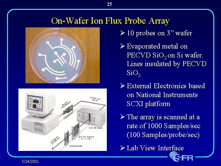
25 On-Wafer Ion Flux Probe Array Ø 10 probes on 3” wafer Ø Evaporated metal on PECVD Si. O 2 on Si wafer. Lines insulated by PECVD Si. O 2 Ø External Electronics based on National Instruments SCXI platform Ø The array is scanned at a rate of 1000 Samples/sec (100 Samples/probe/sec) Ø Lab View Interface 5/24/2001

26 Plasma Instability: J+ (r, q, t) t=0 s t = 1. 5 s t = 3. 2 s t = 4. 5 s 5/24/2001

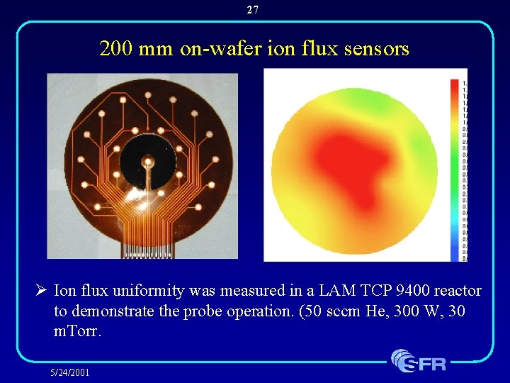
27 200 mm on-wafer ion flux sensors Ø Ion flux uniformity was measured in a LAM TCP 9400 reactor to demonstrate the probe operation. (50 sccm He, 300 W, 30 m. Torr. 5/24/2001

28 Specific Goals Ø Modify data acquisition to be used with rf bias on the electrostatic chuck. Ø Use the probe array to study the factors that affect the plasma and etching uniformity in Cl 2/O 2 etching of Si. Ø Specifically, the goal will be to understand the role of à etching products à the wall conditions à feed gas composition 5/24/2001

29 Microstructures for PECVD Temperature Mapping Dwight Howard, Eunice Lee, Scott D. Collins and Rosemary L. Smith Micro. Instruments and Systems Laboratory (MISL) UC Davis Small Feature Reproducibility: film thickness uniformity is critical Uniformity depends on spatial control of: – plasma composition (gas flow rates and pressure) – plasma energy (power) – substrate surface Temperature -- Project Goals -Design, fabricate and test thin film microstuctures for mapping surface temperature during PECVD, for process monitoring. – minimize tool hardware modifications – process compatibility – low cost manufacture, and data retrieval 5/24/2001

30 Milestones (1 year project) • September 30 th, 2001 – To test thin film resistor sensor array in PECVD. – To design and fabricate MEMS sensor array to record surface temperature variations. – Bench test MEMS array 5/24/2001

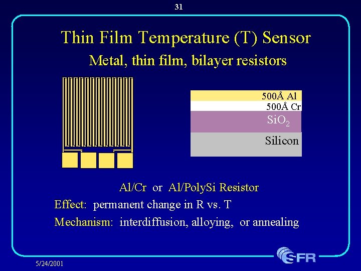
31 Thin Film Temperature (T) Sensor Metal, thin film, bilayer resistors 500Å Al 500Å Cr Si. O 2 Silicon Al/Cr or Al/Poly. Si Resistor Effect: permanent change in R vs. T Mechanism: interdiffusion, alloying, or annealing 5/24/2001

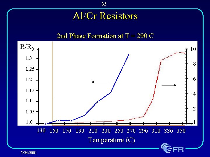
32 Al/Cr Resistors 2 nd Phase Formation at T = 290 C R/R 0 10 1. 3 8 1. 25 6 1. 2 1. 15 4 1. 1 2 1. 05 1 1. 0 130 150 170 190 210 230 250 270 290 310 330 350 Temperature (C) 5/24/2001

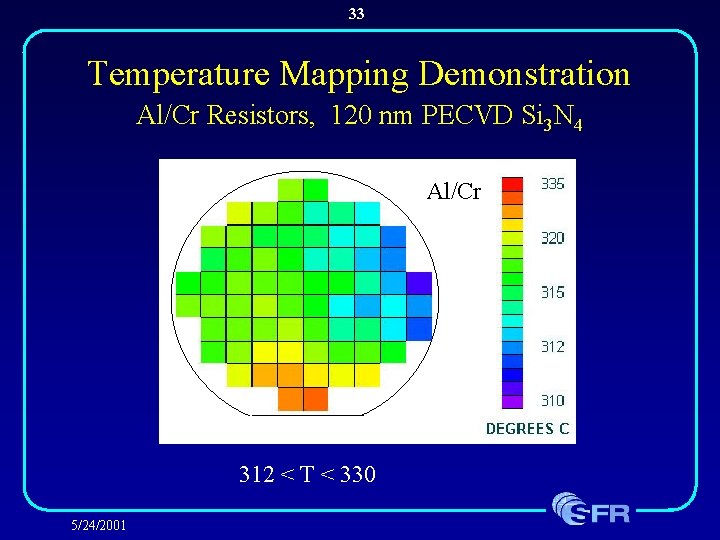
33 Temperature Mapping Demonstration Al/Cr Resistors, 120 nm PECVD Si 3 N 4 Al/Cr 312 < T < 330 5/24/2001

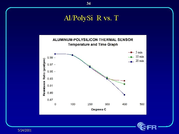
34 Al/Poly. Si R vs. T 5 min 10 min 20 min 5/24/2001

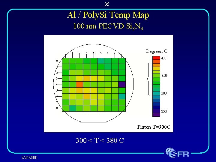
35 Al / Poly. Si Temp Map 100 nm PECVD Si 3 N 4 Degrees, C 400 350 300 250 Platen T=300 C 300 < T < 380 C 5/24/2001

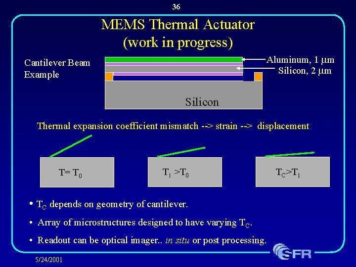
36 MEMS Thermal Actuator (work in progress) Aluminum, 1 mm Silicon, 2 mm Cantilever Beam Example Silicon Thermal expansion coefficient mismatch --> strain --> displacement T= T 0 T 1 >T 0 • TC depends on geometry of cantilever. • Array of microstructures designed to have varying TC. • Readout can be optical imager. . in situ or post processing. 5/24/2001 TC>T 1

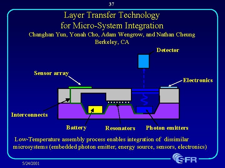
37 Layer Transfer Technology for Micro-System Integration Changhan Yun, Yonah Cho, Adam Wengrow, and Nathan Cheung Berkeley, CA Detector Sensor array Electronics Interconnects Battery Resonators Photon emitters Low-Temperature assembly process enables integration of dissimilar microsystems (embedded photon emitter, energy source, sensors, electronics) 5/24/2001

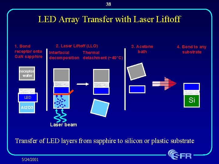
38 LED Array Transfer with Laser Liftoff 1. Bond receptor onto Ga. N sapphire 2. Laser Liftoff (LLO) Thermal Interfacial decomposition detachment (~40°C) 3. Acetone bath 4. Bond to any substrate receptor wafer adhesive LED Si Al 2 O 3 Laser beam Transfer of LED layers from sapphire to silicon or plastic substrate 5/24/2001

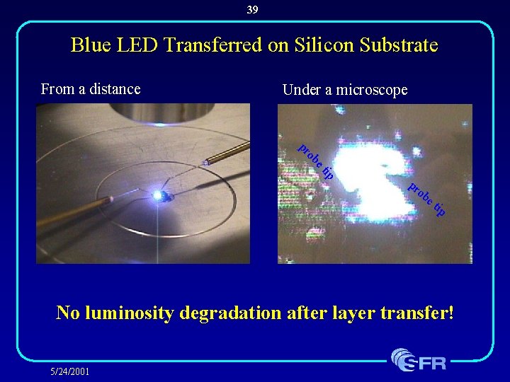
39 Blue LED Transferred on Silicon Substrate From a distance Under a microscope ip et ob pr pr ob et ip No luminosity degradation after layer transfer! 5/24/2001

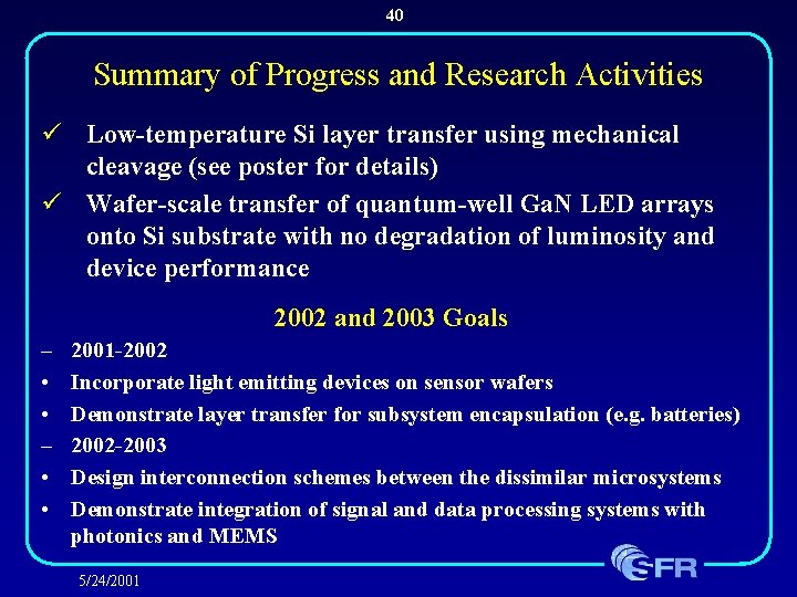
40 Summary of Progress and Research Activities ü Low-temperature Si layer transfer using mechanical cleavage (see poster for details) ü Wafer-scale transfer of quantum-well Ga. N LED arrays onto Si substrate with no degradation of luminosity and device performance 2002 and 2003 Goals – • • 2001 -2002 Incorporate light emitting devices on sensor wafers Demonstrate layer transfer for subsystem encapsulation (e. g. batteries) 2002 -2003 Design interconnection schemes between the dissimilar microsystems Demonstrate integration of signal and data processing systems with photonics and MEMS 5/24/2001

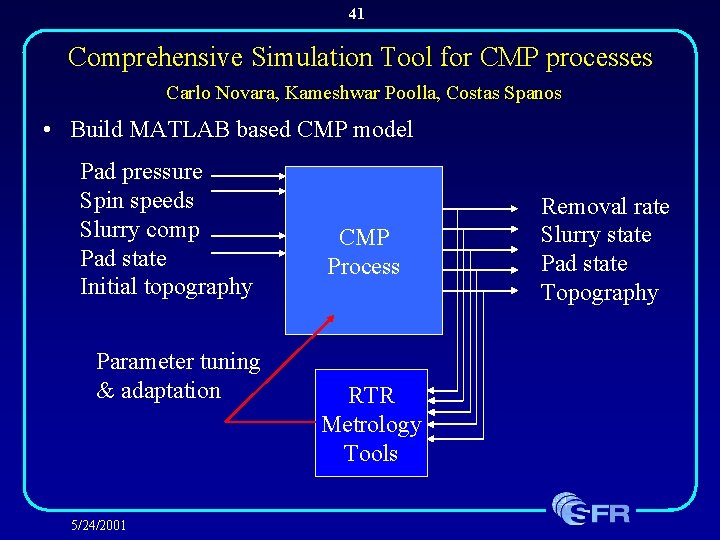
41 Comprehensive Simulation Tool for CMP processes Carlo Novara, Kameshwar Poolla, Costas Spanos • Build MATLAB based CMP model Pad pressure Spin speeds Slurry comp Pad state Initial topography Parameter tuning & adaptation 5/24/2001 CMP Process RTR Metrology Tools Removal rate Slurry state Pad state Topography

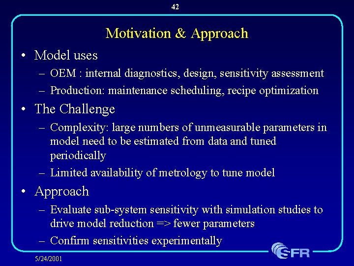
42 Motivation & Approach • Model uses – OEM : internal diagnostics, design, sensitivity assessment – Production: maintenance scheduling, recipe optimization • The Challenge – Complexity: large numbers of unmeasurable parameters in model need to be estimated from data and tuned periodically – Limited availability of metrology to tune model • Approach – Evaluate sub-system sensitivity with simulation studies to drive model reduction => fewer parameters – Confirm sensitivities experimentally 5/24/2001

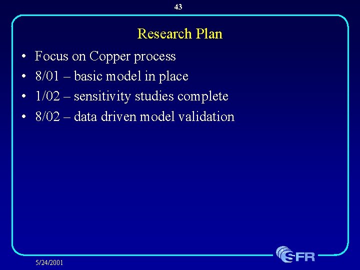
43 Research Plan • • Focus on Copper process 8/01 – basic model in place 1/02 – sensitivity studies complete 8/02 – data driven model validation 5/24/2001

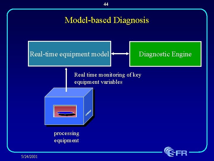
44 Model-based Diagnosis Real-time equipment model Diagnostic Engine Real time monitoring of key equipment variables processing equipment 5/24/2001

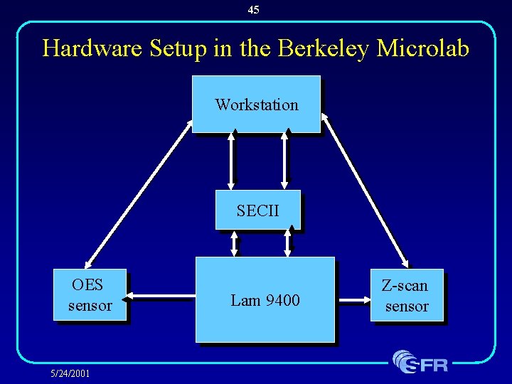
45 Hardware Setup in the Berkeley Microlab Workstation SECII OES sensor 5/24/2001 Lam 9400 Z-scan sensor

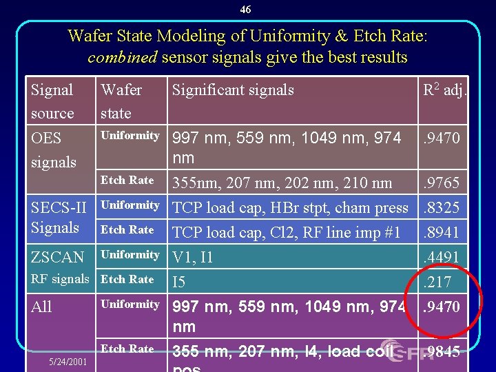
46 Wafer State Modeling of Uniformity & Etch Rate: combined sensor signals give the best results Signal source OES signals Wafer state Significant signals R 2 adj. Uniformity 997 nm, 559 nm, 1049 nm, 974 nm 355 nm, 207 nm, 202 nm, 210 nm TCP load cap, HBr stpt, cham press TCP load cap, Cl 2, RF line imp #1 V 1, I 1 I 5 . 9470 Etch Rate SECS-II Signals Uniformity ZSCAN Uniformity Etch Rate RF signals Etch Rate All Uniformity Etch Rate 5/24/2001 . 9765. 8325. 8941. 4491. 217 997 nm, 559 nm, 1049 nm, 974. 9470 nm. 9845 355 nm, 207 nm, I 4, load coil

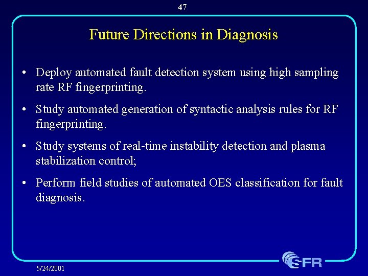
47 Future Directions in Diagnosis • Deploy automated fault detection system using high sampling rate RF fingerprinting. • Study automated generation of syntactic analysis rules for RF fingerprinting. • Study systems of real-time instability detection and plasma stabilization control; • Perform field studies of automated OES classification for fault diagnosis. 5/24/2001

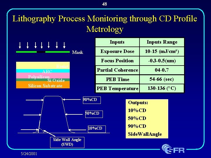
48 Lithography Process Monitoring through CD Profile Metrology Inputs Range Exposure Dose 10 -15 (m. J/cm²) Focus Position -0. 3 -0. 5(um) Partial Coherence 04 -0. 7 PEB Time 54 -66 (sec) PEB Temperature 130 -136 (°C) Mask Resist ARC Polysilicon Si Oxide Silicon Substrate 90%CD 50%CD 10%CD Side Wall Angle (SWD) 5/24/2001 Outputs: 10%CD 50%CD 90%CD Side. Wall. Angle

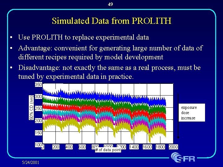
49 Simulated Data from PROLITH • Use PROLITH to replace experimental data • Advantage: convenient for generating large number of data of different recipes required by model development • Disadvantage: not exactly the same as a real process, must be tuned by experimental data in practice. 50% CD (nm) 350 300 exposure dose increase 250 200 150 100 0 5/24/2001 200 400 600 800 1000 1200 1400 # of data point 1600 1800 2000

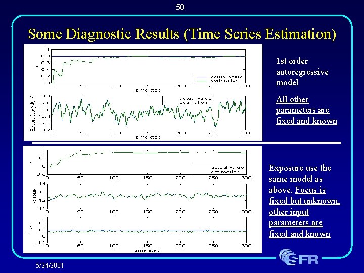
50 Some Diagnostic Results (Time Series Estimation) 1 st order autoregressive model All other parameters are fixed and known Exposure use the same model as above. Focus is fixed but unknown, other input parameters are fixed and known 5/24/2001

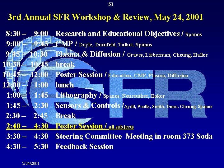
51 3 rd Annual SFR Workshop & Review, May 24, 2001 8: 30 – 9: 00 – 9: 45 – 10: 30 – 10: 45 – 12: 00 – 1: 45 – 2: 30 – 2: 40 – 3: 30 – 4: 30 – 9: 00 9: 45 10: 30 10: 45 12: 00 1: 45 2: 30 2: 45 4: 30 5: 30 5/24/2001 Research and Educational Objectives / Spanos CMP / Doyle, Dornfeld, Talbot, Spanos Plasma & Diffusion / Graves, Lieberman, Cheung, Haller break Poster Session / Education, CMP, Plasma, Diffusion lunch Lithography / Spanos, Neureuther, Bokor Sensors & Controls /Aydil, Poolla, Smith, Dunn, Cheung, Spanos Break Poster Session / all subjects Steering Committee Meeting in room 373 Soda Feedback Session