1 On Wafer Ion Flux Sensors SFR Workshop
- Slides: 9

1 On Wafer Ion Flux Sensors SFR Workshop May 24, 2001 Berkeley, CA Tae Won Kim, Saurabh Ullal, and Eray S Aydil University of California Santa Barbara 2001 GOAL: Build and demonstrate Langmuir probe based on wafer ion flux probe array using external electronics by 9/30/2001. 5/24/2001

2 Motivation and Goals • Variation of ion bombardment flux and its spatial distribution with plasma conditions is critical to plasma etching. • Ion flux uniformity at the wafer determines the uniformity of etching and etching profile evolution. • There have been almost no measurements of the ion flux or ion flux distribution across the wafer as a function of both r and q in realistic etching chemistry. • Design, build, and demonstrate an on-wafer ion flux analyzer with external electronics capable of mapping J+ (r, q) on a wafer. 5/24/2001

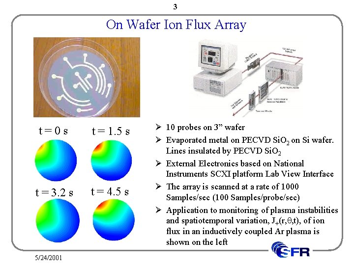
3 On Wafer Ion Flux Array t=0 s t = 1. 5 s t = 3. 2 s t = 4. 5 s 5/24/2001 Ø 10 probes on 3” wafer Ø Evaporated metal on PECVD Si. O 2 on Si wafer. Lines insulated by PECVD Si. O 2 Ø External Electronics based on National Instruments SCXI platform Lab View Interface Ø The array is scanned at a rate of 1000 Samples/sec (100 Samples/probe/sec) Ø Application to monitoring of plasma instabilities and spatiotemporal variation, J+(r, q, t), of ion flux in an inductively coupled Ar plasma is shown on the left

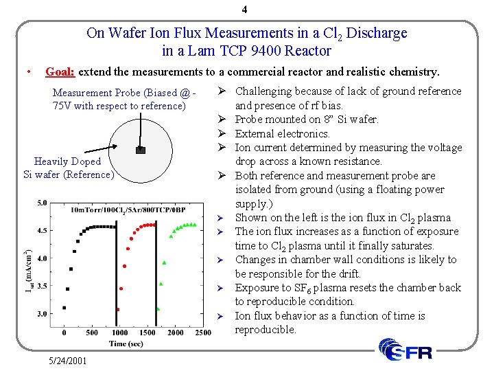
4 On Wafer Ion Flux Measurements in a Cl 2 Discharge in a Lam TCP 9400 Reactor • Goal: extend the measurements to a commercial reactor and realistic chemistry. Measurement Probe (Biased @ 75 V with respect to reference) Heavily Doped Si wafer (Reference) 5/24/2001 Ø Challenging because of lack of ground reference and presence of rf bias. Ø Probe mounted on 8” Si wafer. Ø External electronics. Ø Ion current determined by measuring the voltage drop across a known resistance. Ø Both reference and measurement probe are isolated from ground (using a floating power supply. ) Ø Shown on the left is the ion flux in Cl 2 plasma Ø The ion flux increases as a function of exposure time to Cl 2 plasma until it finally saturates. Ø Changes in chamber wall conditions is likely to be responsible for the drift. Ø Exposure to SF 6 plasma resets the chamber back to reproducible condition. Ø Ion flux behavior as a function of time is reproducible.

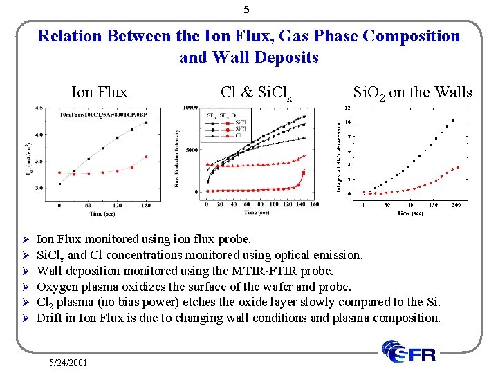
5 Relation Between the Ion Flux, Gas Phase Composition and Wall Deposits Ion Flux Ø Ø Ø Cl & Si. Clx Si. O 2 on the Walls Ion Flux monitored using ion flux probe. Si. Clx and Cl concentrations monitored using optical emission. Wall deposition monitored using the MTIR-FTIR probe. Oxygen plasma oxidizes the surface of the wafer and probe. Cl 2 plasma (no bias power) etches the oxide layer slowly compared to the Si. Drift in Ion Flux is due to changing wall conditions and plasma composition. 5/24/2001

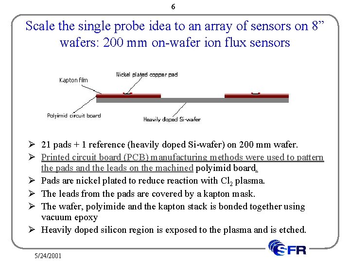
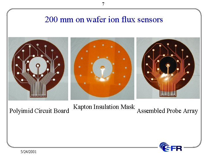
6 Scale the single probe idea to an array of sensors on 8” wafers: 200 mm on-wafer ion flux sensors Ø 21 pads + 1 reference (heavily doped Si-wafer) on 200 mm wafer. Ø Printed circuit board (PCB) manufacturing methods were used to pattern the pads and the leads on the machined polyimid board. Ø Pads are nickel plated to reduce reaction with Cl 2 plasma. Ø The leads from the pads are covered by a kapton mask. Ø The wafer, polyimide and the kapton stack is bonded together using vacuum epoxy Ø Heavily doped silicon region is exposed to the plasma and is etched. 5/24/2001

7 200 mm on wafer ion flux sensors Polyimid Circuit Board 5/24/2001 Kapton Insulation Mask Assembled Probe Array

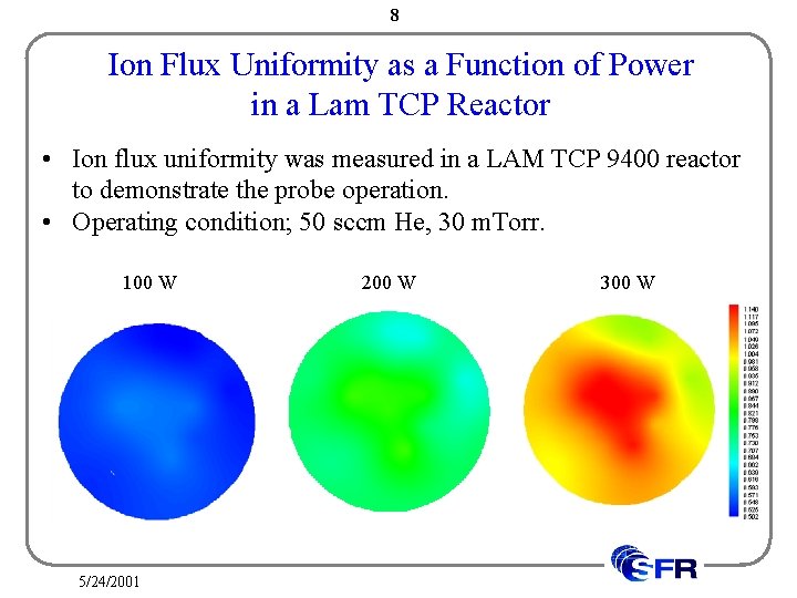
8 Ion Flux Uniformity as a Function of Power in a Lam TCP Reactor • Ion flux uniformity was measured in a LAM TCP 9400 reactor to demonstrate the probe operation. • Operating condition; 50 sccm He, 30 m. Torr. 100 W 5/24/2001 200 W 300 W

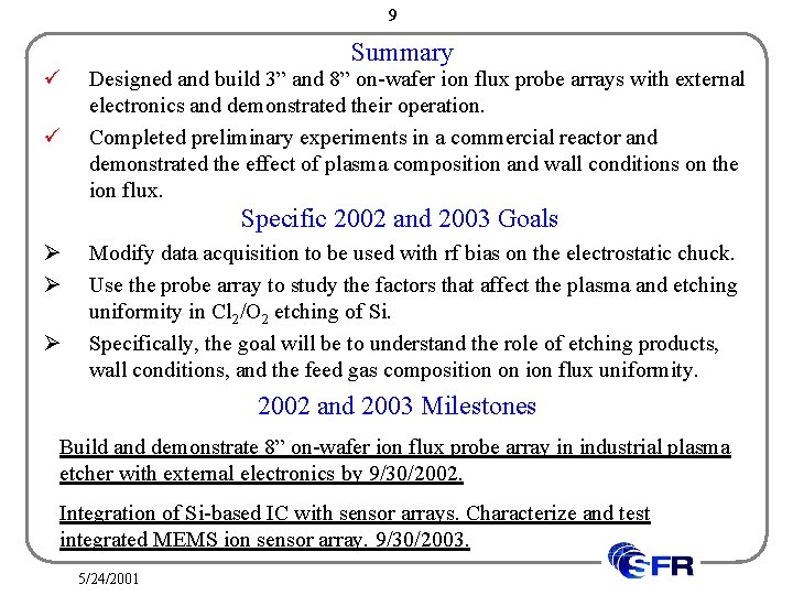
9 ü ü Summary Designed and build 3” and 8” on-wafer ion flux probe arrays with external electronics and demonstrated their operation. Completed preliminary experiments in a commercial reactor and demonstrated the effect of plasma composition and wall conditions on the ion flux. Specific 2002 and 2003 Goals Ø Ø Ø Modify data acquisition to be used with rf bias on the electrostatic chuck. Use the probe array to study the factors that affect the plasma and etching uniformity in Cl 2/O 2 etching of Si. Specifically, the goal will be to understand the role of etching products, wall conditions, and the feed gas composition on ion flux uniformity. 2002 and 2003 Milestones Build and demonstrate 8” on-wafer ion flux probe array in industrial plasma etcher with external electronics by 9/30/2002. Integration of Si-based IC with sensor arrays. Characterize and test integrated MEMS ion sensor array. 9/30/2003. 5/24/2001