Zero Voltage Switching Quasiresonant Converters EE 4211 1
- Slides: 52

Zero Voltage Switching Quasi-resonant Converters EE 4211 1

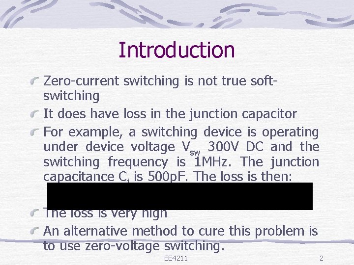
Introduction Zero-current switching is not true softswitching It does have loss in the junction capacitor For example, a switching device is operating under device voltage Vsw 300 V DC and the switching frequency is 1 MHz. The junction capacitance Cj is 500 p. F. The loss is then: The loss is very high An alternative method to cure this problem is to use zero-voltage switching. EE 4211 2

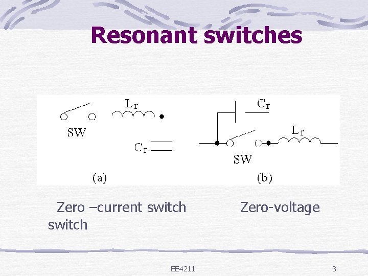
Resonant switches Zero –current switch EE 4211 Zero-voltage 3

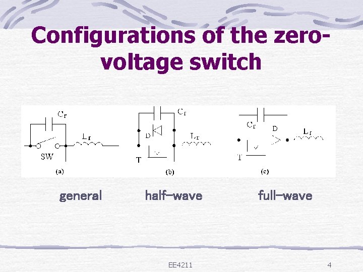
Configurations of the zerovoltage switch general half-wave EE 4211 full-wave 4

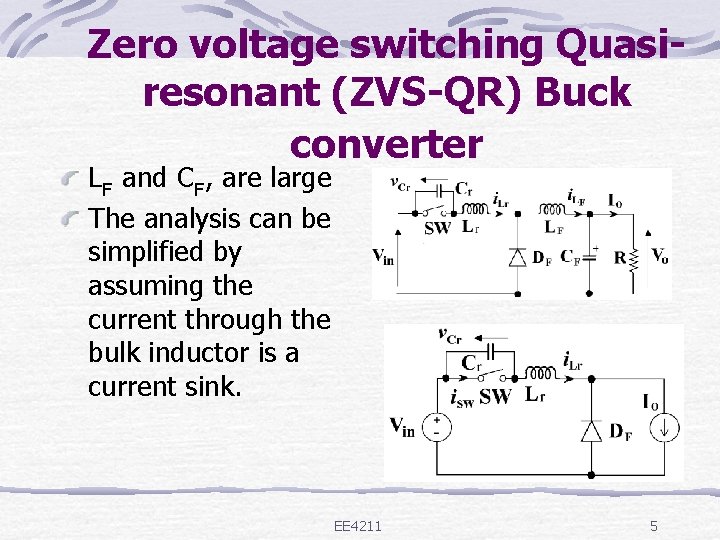
Zero voltage switching Quasiresonant (ZVS-QR) Buck converter LF and CF, are large The analysis can be simplified by assuming the current through the bulk inductor is a current sink. EE 4211 5

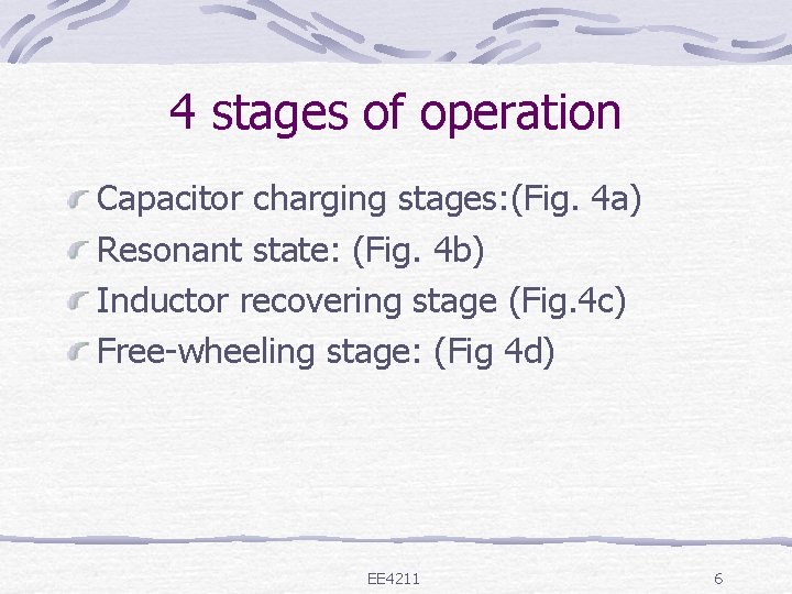
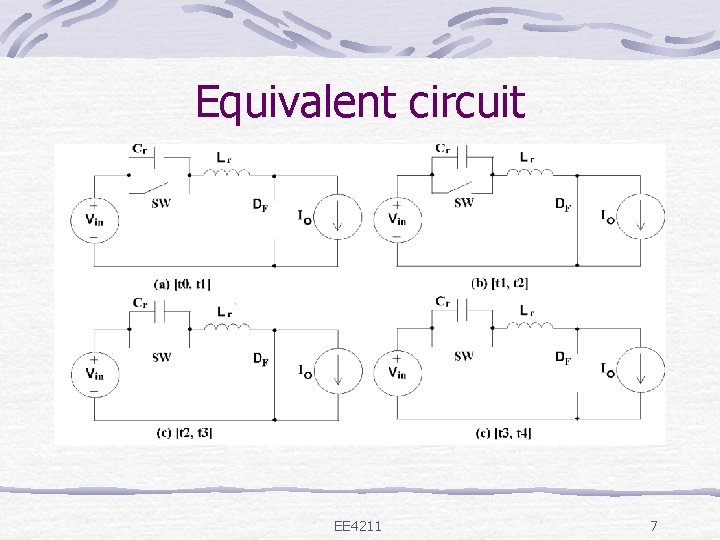
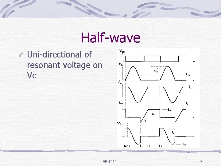
4 stages of operation Capacitor charging stages: (Fig. 4 a) Resonant state: (Fig. 4 b) Inductor recovering stage (Fig. 4 c) Free-wheeling stage: (Fig 4 d) EE 4211 6

Equivalent circuit EE 4211 7

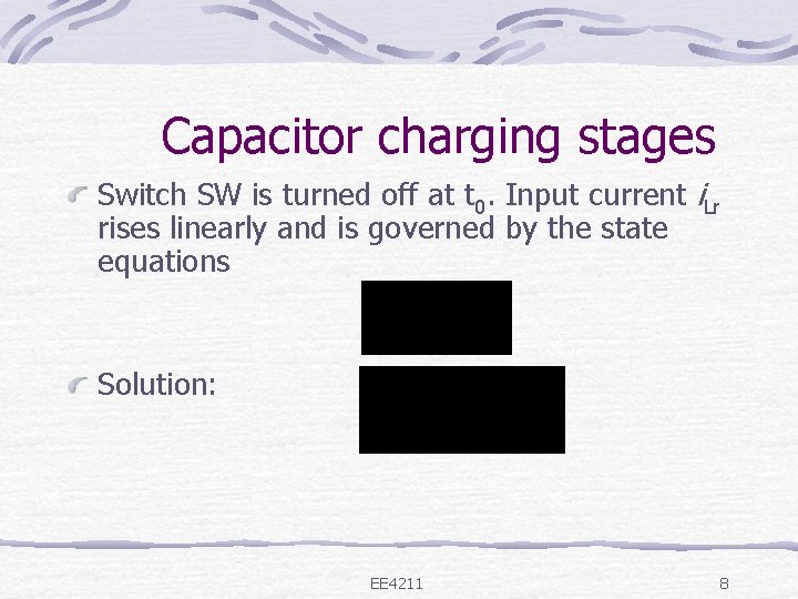
Capacitor charging stages Switch SW is turned off at t 0. Input current i. Lr rises linearly and is governed by the state equations Solution: EE 4211 8

Half-wave Uni-directional of resonant voltage on Vc EE 4211 9

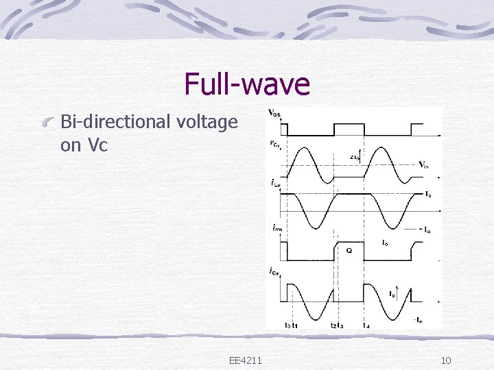
Full-wave Bi-directional voltage on Vc EE 4211 10

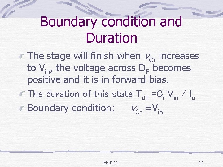
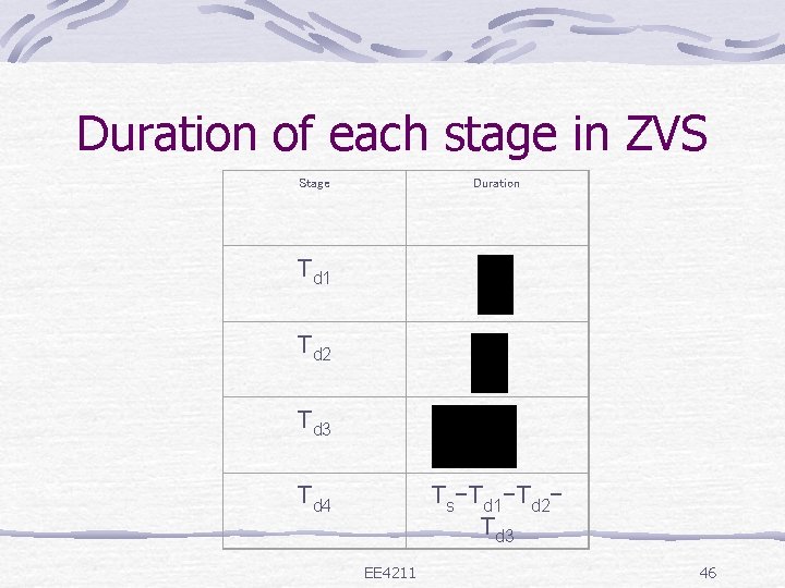
Boundary condition and Duration The stage will finish when v. Cr increases to Vin, the voltage across DF becomes positive and it is in forward bias. The duration of this state Td 1 =Cr Vin / Io Boundary condition: v. Cr =Vin EE 4211 11

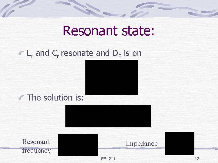
Resonant state: Lr and Cr resonate and DF is on The solution is: Resonant frequency Impedance EE 4211 12

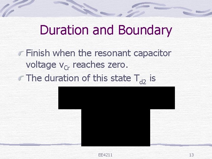
Duration and Boundary Finish when the resonant capacitor voltage v. Cr reaches zero. The duration of this state Td 2 is EE 4211 13

Termination of resonant stage The termination of this state is similar to the zerocurrent switching. For the half-wave mode, when resonant voltage v. Cr reaches zero, it cannot be reversed because the anti-parallel diode D of the switch conducts. The transistor T of the switch SW can be turned on after that to achieve zero-voltage switching. For full-wave mode, v. Cr can reverse into negative because there is a series diode D with the transistor T. During v. Cr is negative, the transistor T should be turned off. When v. Cr resonates back from negative to zero, since T is EE 4211 stops. 14 already off, the resonance

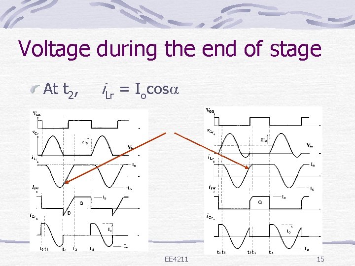
Voltage during the end of stage At t 2, i. Lr = Iocos EE 4211 15

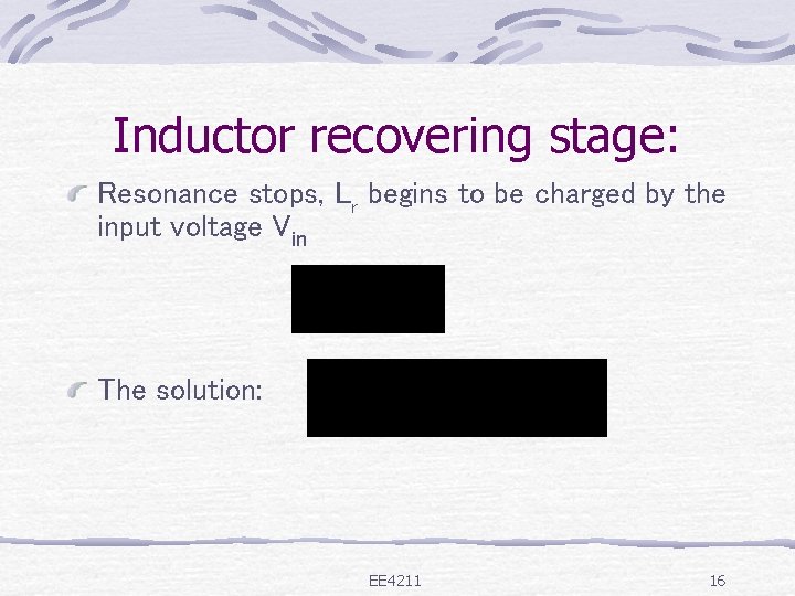
Inductor recovering stage: Resonance stops, Lr begins to be charged by the input voltage Vin The solution: EE 4211 16

Finish of this stage Finish when i. Lr reaches the value of output current IO. DF no longer conducts because its current is now all conducted by Lr. Duration: Td 3 = Lr Io cos / Vin Boundary condition: i. Lr=Io EE 4211 17

Free-wheeling stage: (Fig 4 d) Output current freewheels through Lr and switch SW. This stage finishes when the transistor turns off again at t 4 is the same as t 0 in next cycle. Duration: Td 4= Ts-Td 1 -Td 2 -Td 3 where Ts is the period of the switching cycle. EE 4211 18

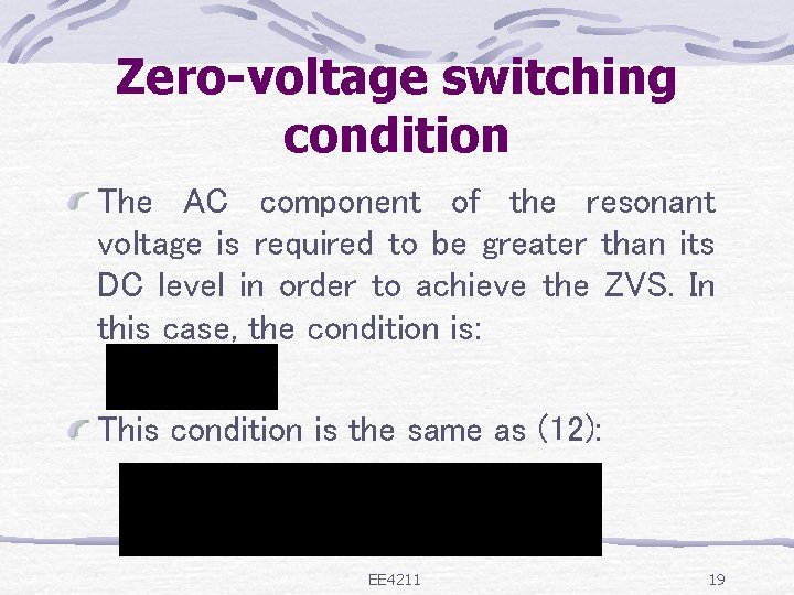
Zero-voltage switching condition The AC component of the resonant voltage is required to be greater than its DC level in order to achieve the ZVS. In this case, the condition is: This condition is the same as (12): EE 4211 19

Zero-voltage switching When to turn on and off The instant to turn on the switch is also important. For half-wave mode, the transistor must be turned on after v. Cr reaches zero at t 2 and before isw increases back to positive. For full-wave mode, the transistor must be turned on when v. Cr is negative. When T is turned on, the series diode D is still in reverse bias and the voltage across T is virtually zero. EE 4211 20

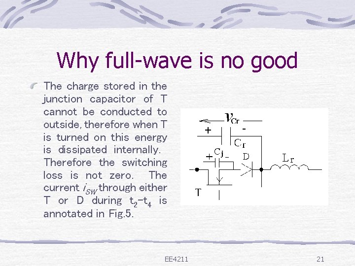
Why full-wave is no good The charge stored in the junction capacitor of T cannot be conducted to outside, therefore when T is turned on this energy is dissipated internally. Therefore the switching loss is not zero. The current i. SW through either T or D during t 2 -t 4 is annotated in Fig. 5. EE 4211 21

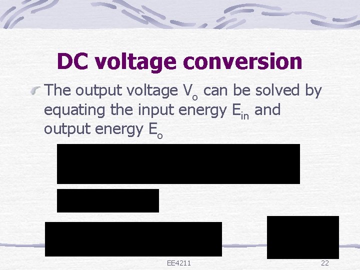
DC voltage conversion The output voltage Vo can be solved by equating the input energy Ein and output energy Eo EE 4211 22

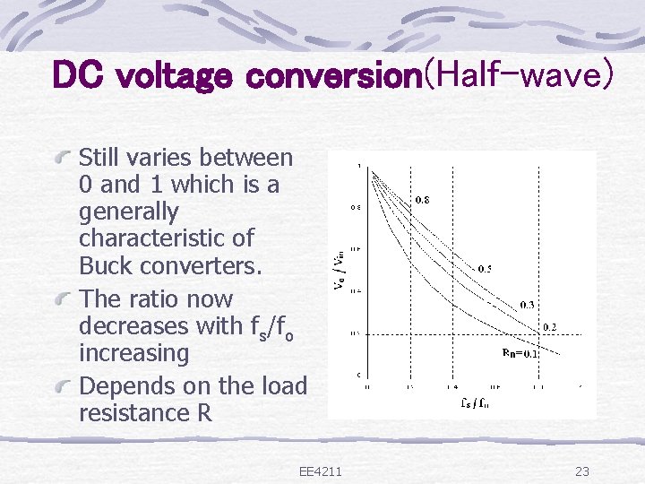
DC voltage conversion(Half-wave) Still varies between 0 and 1 which is a generally characteristic of Buck converters. The ratio now decreases with fs/fo increasing Depends on the load resistance R EE 4211 23

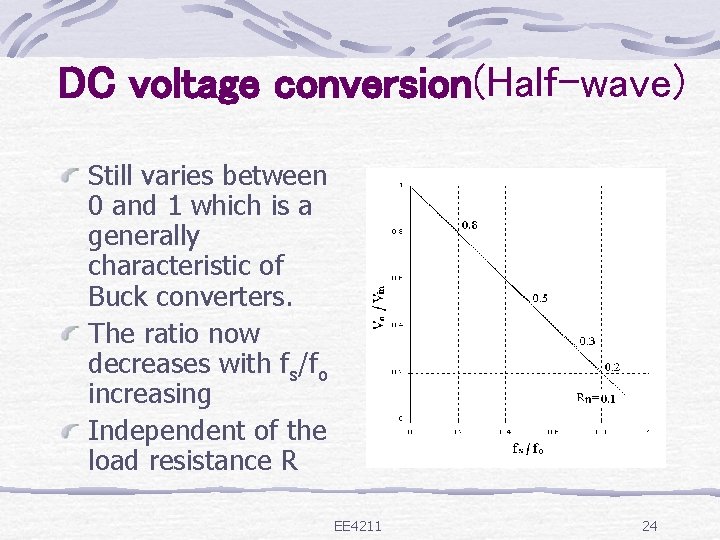
DC voltage conversion(Half-wave) Still varies between 0 and 1 which is a generally characteristic of Buck converters. The ratio now decreases with fs/fo increasing Independent of the load resistance R EE 4211 24

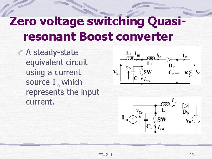
Zero voltage switching Quasiresonant Boost converter A steady-state equivalent circuit using a current source Iin which represents the input current. EE 4211 25

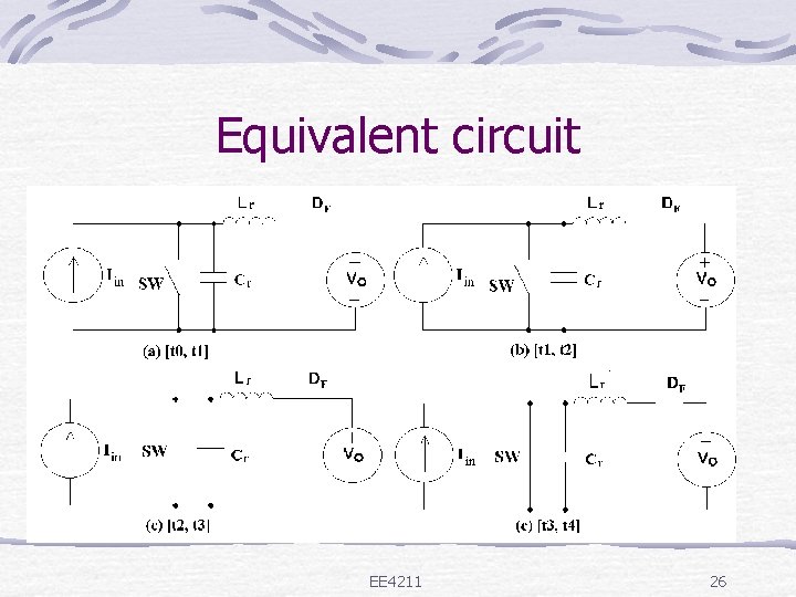
Equivalent circuit EE 4211 26

4 stages of operation Capacitor charging stages: (Fig. 8 a) Resonant state: (Fig. 8 b) Inductor recovering stage (Fig. 8 c) Free-wheeling stage: (Fig 8 d) EE 4211 27

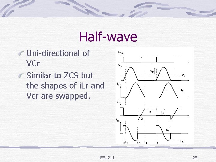
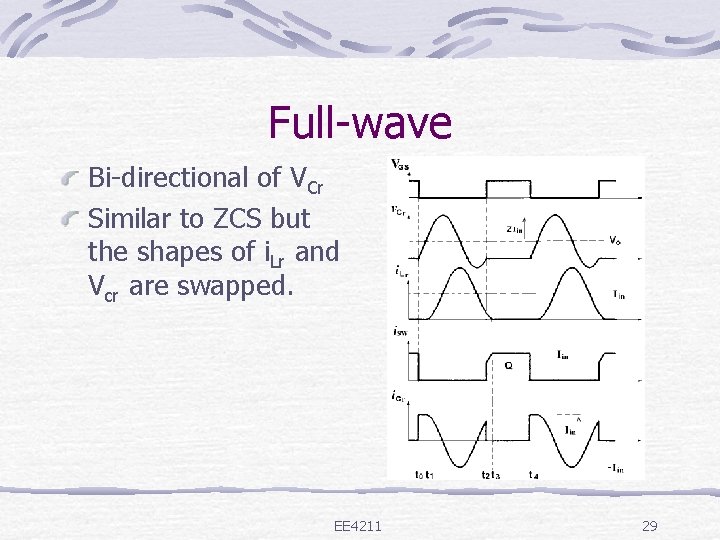
Half-wave Uni-directional of VCr Similar to ZCS but the shapes of i. Lr and Vcr are swapped. EE 4211 28

Full-wave Bi-directional of VCr Similar to ZCS but the shapes of i. Lr and Vcr are swapped. EE 4211 29

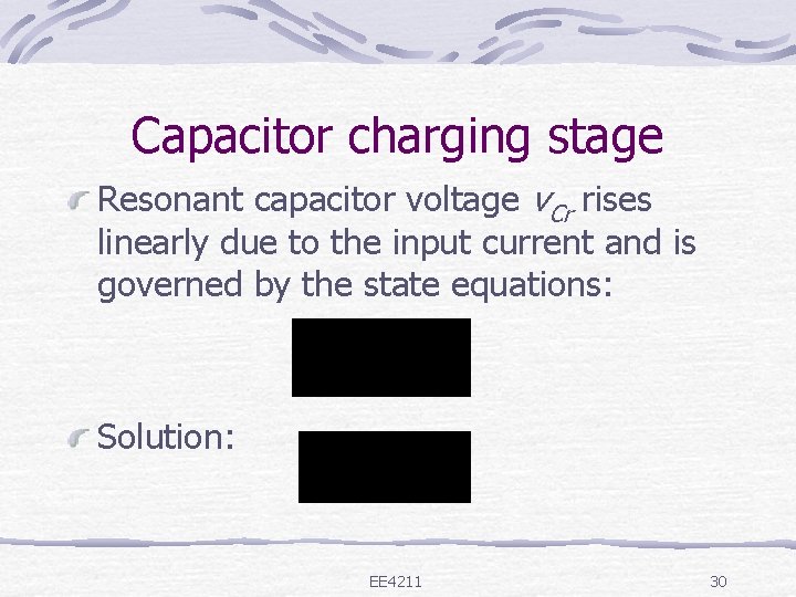
Capacitor charging stage Resonant capacitor voltage v. Cr rises linearly due to the input current and is governed by the state equations: Solution: EE 4211 30

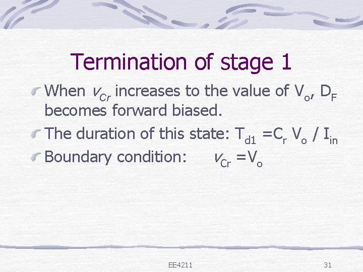
Termination of stage 1 When v. Cr increases to the value of Vo, DF becomes forward biased. The duration of this state: Td 1 =Cr Vo / Iin Boundary condition: v. Cr =Vo EE 4211 31

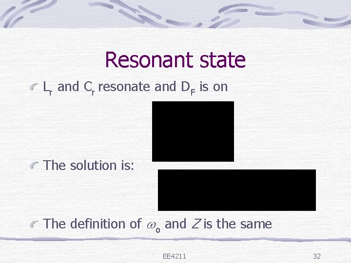
Resonant state Lr and Cr resonate and DF is on The solution is: The definition of o and Z is the same EE 4211 32

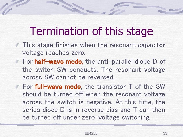
Termination of this stage This stage finishes when the resonant capacitor voltage reaches zero. For half-wave mode, the anti-parallel diode D of the switch SW conducts. The resonant voltage across SW cannot be reversed. For full-wave mode, the transistor T of the SW should be turned off when the resonant voltage across the switch is negative. At this time, the series diode D is in reverse bias and T can then be turned off under zero-voltage switching. EE 4211 33

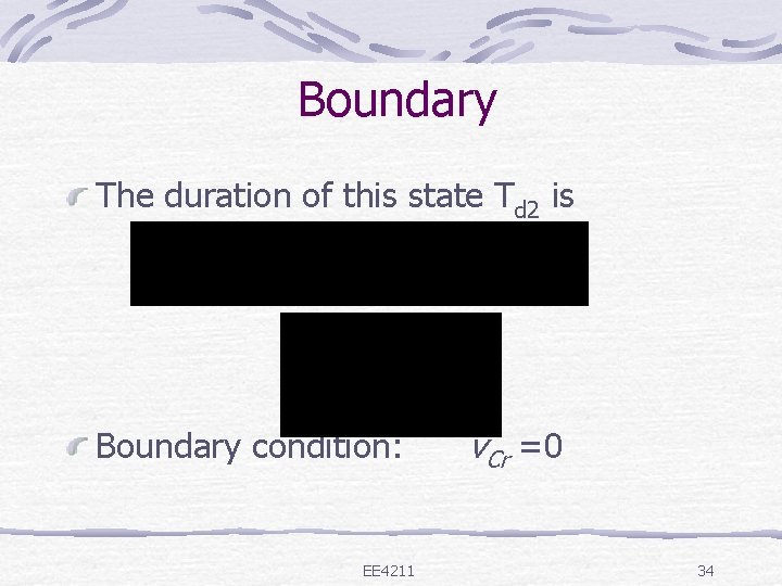
Boundary The duration of this state Td 2 is Boundary condition: EE 4211 v. Cr =0 34

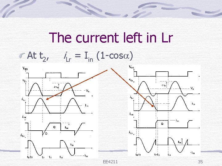
The current left in Lr At t 2, i. Lr = Iin (1 -cos ) EE 4211 35

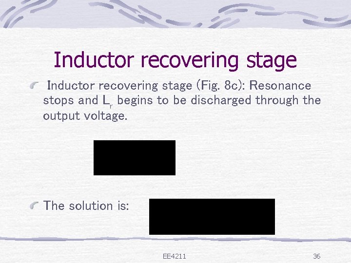
Inductor recovering stage (Fig. 8 c): Resonance stops and Lr begins to be discharged through the output voltage. The solution is: EE 4211 36

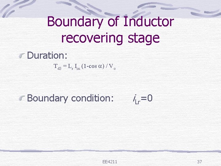
Boundary of Inductor recovering stage Duration: Td 3 = Lr Iin (1 -cos ) / Vo Boundary condition: EE 4211 i. Lr=0 37

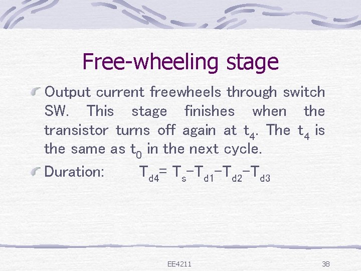
Free-wheeling stage Output current freewheels through switch SW. This stage finishes when the transistor turns off again at t 4. The t 4 is the same as t 0 in the next cycle. Duration: Td 4= Ts-Td 1 -Td 2 -Td 3 EE 4211 38

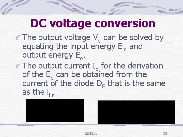
DC voltage conversion The output voltage Vo can be solved by equating the input energy Ein and output energy Eo. The output current Io for the derivation of the Eo can be obtained from the current of the diode DF that is the same as the i. Lr EE 4211 39

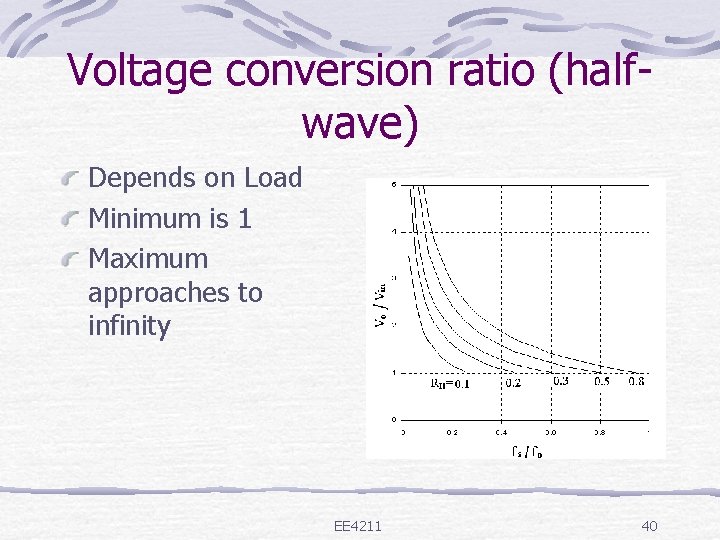
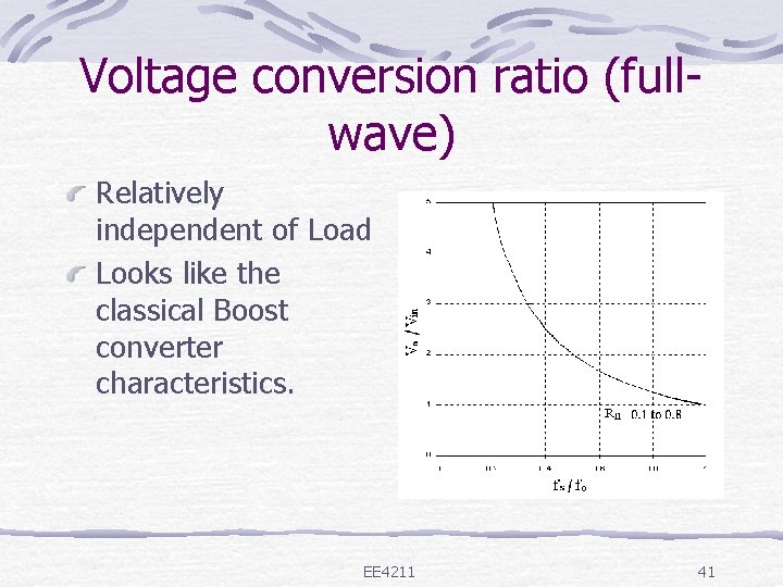
Voltage conversion ratio (halfwave) Depends on Load Minimum is 1 Maximum approaches to infinity EE 4211 40

Voltage conversion ratio (fullwave) Relatively independent of Load Looks like the classical Boost converter characteristics. EE 4211 41

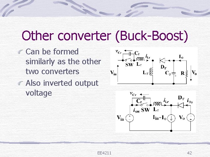
Other converter (Buck-Boost) Can be formed similarly as the other two converters Also inverted output voltage EE 4211 42

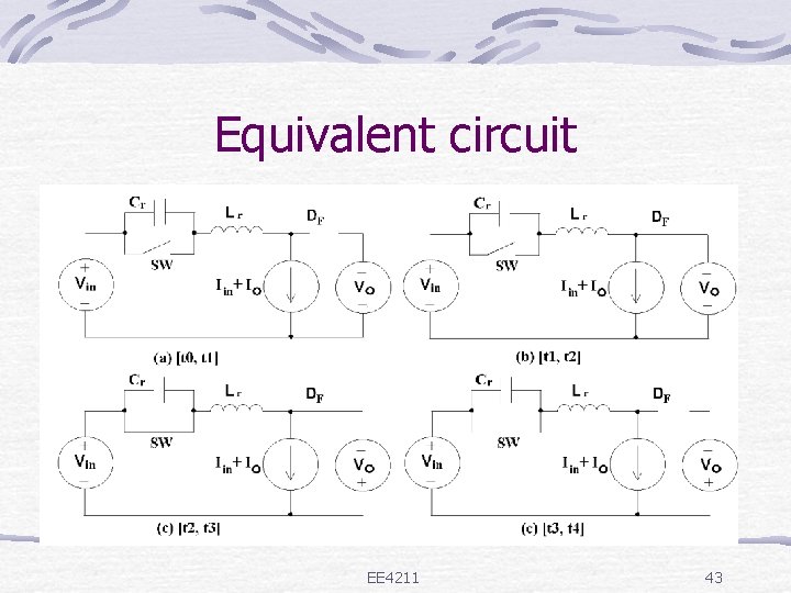
Equivalent circuit EE 4211 43

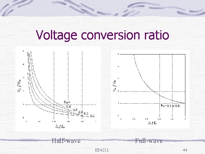
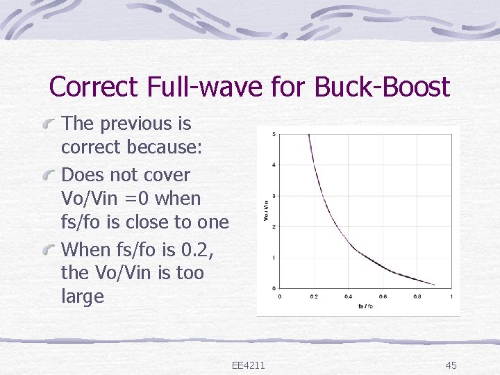
Voltage conversion ratio Half-wave Full-wave EE 4211 44

Correct Full-wave for Buck-Boost The previous is correct because: Does not cover Vo/Vin =0 when fs/fo is close to one When fs/fo is 0. 2, the Vo/Vin is too large EE 4211 45

Duration of each stage in ZVS Stage Duration Td 1 Td 2 Td 3 Td 4 Ts-Td 1 -Td 2 Td 3 EE 4211 46

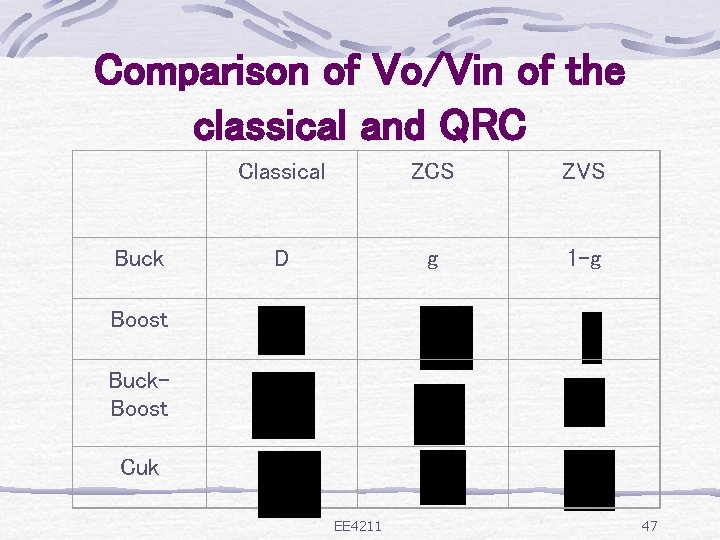
Comparison of Vo/Vin of the classical and QRC Classical ZCS ZVS Buck D g 1 -g Boost Buck. Boost Cuk EE 4211 47

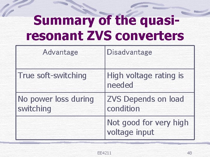
Summary of the quasiresonant ZVS converters Advantage Disadvantage True soft-switching High voltage rating is needed No power loss during switching ZVS Depends on load condition Not good for very high voltage input EE 4211 48

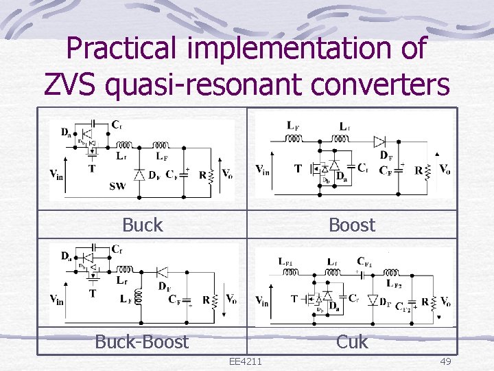
Practical implementation of ZVS quasi-resonant converters Buck Boost Buck-Boost Cuk EE 4211 49

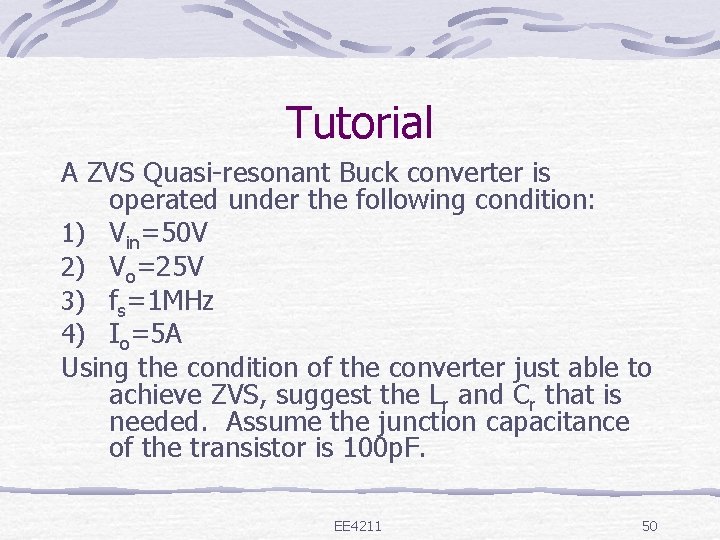
Tutorial A ZVS Quasi-resonant Buck converter is operated under the following condition: 1) Vin=50 V 2) Vo=25 V 3) fs=1 MHz 4) Io=5 A Using the condition of the converter just able to achieve ZVS, suggest the Lr and Cr that is needed. Assume the junction capacitance of the transistor is 100 p. F. EE 4211 50

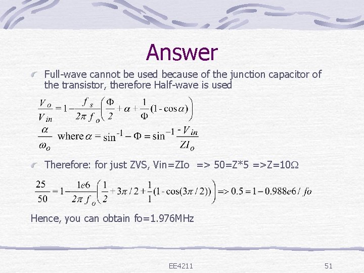
Answer Full-wave cannot be used because of the junction capacitor of the transistor, therefore Half-wave is used Therefore: for just ZVS, Vin=ZIo => 50=Z*5 =>Z=10 Hence, you can obtain fo=1. 976 MHz EE 4211 51

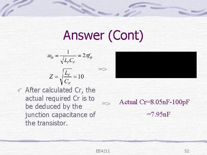
Answer (Cont) => After calculated Cr, the actual required Cr is to => be deduced by the junction capacitance of the transistor. EE 4211 Actual Cr=8. 05 n. F-100 p. F =7. 95 n. F 52