LEC11 VOLTAGE REGULATORS Typical Unregulated DC Voltage Voltage
- Slides: 19

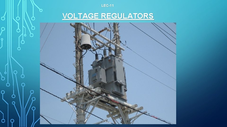
LEC-11 VOLTAGE REGULATORS

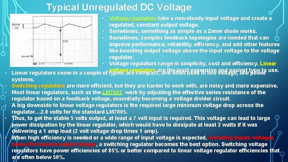
Typical Unregulated DC Voltage • Voltage regulators take a non-steady input voltage and create a regulated, constant output voltage. • Sometimes, something as simple as a Zener diode works. • Sometimes, complex feedback topologies are needed that can improve performance, reliability, efficiency, and add other features like boosting output voltage above the input voltage to the voltage regulator. • Voltage regulators range in simplicity, cost and efficiency. Linear voltageare regulators the leastused expensive and easiest to use. • Linear regulators come in a couple of types, compactare , and often in low voltage, low type power systems. • Switching regulators are more efficient, but they are harder to work with, are noisy and more expensive. • Most linear regulators, such as the LM 7805, LM 7805 work by adjusting the effective series resistance of the regulator based on a feedback voltage, essentially becoming a voltage divider circuit. • A big downside to linear voltage regulators is the required large minimum voltage drop across the regulator… 2. 0 volts for the standard LM 7805. • Thus, to get the stable 5 volts output, at least a 7 volt input is required. This voltage can lead to large power dissipation by the linear regulator, which would have to dissipate at least 2 watts if it was delivering a 1 amp load (2 voltage drop times 1 amp). • When high efficiency is needed or a wide range of input voltage is expected, including inputs voltages below the desired output voltage, a switching regulator becomes the best option. Switching voltage regulators have power efficiencies of 85% or better compared to linear voltage regulator efficiencies that are often below 50%.

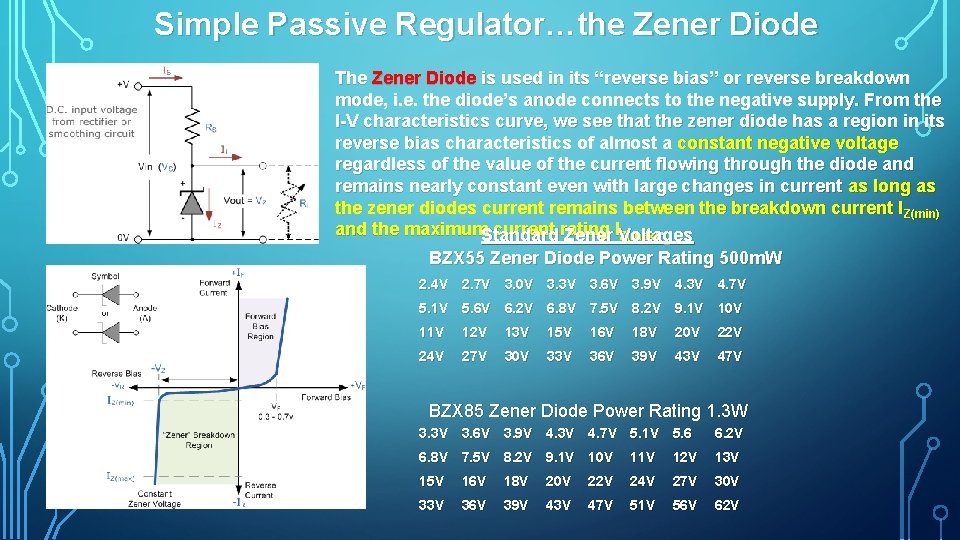
Simple Passive Regulator…the Zener Diode The Zener Diode is used in its “reverse bias” or reverse breakdown mode, i. e. the diode’s anode connects to the negative supply. From the I-V characteristics curve, we see that the zener diode has a region in its reverse bias characteristics of almost a constant negative voltage regardless of the value of the current flowing through the diode and remains nearly constant even with large changes in current as long as the zener diodes current remains between the breakdown current I Z(min) and the maximum. Standard current rating Z(max). Zener IVoltages BZX 55 Zener Diode Power Rating 500 m. W 2. 4 V 2. 7 V 3. 0 V 3. 3 V 3. 6 V 3. 9 V 4. 3 V 4. 7 V 5. 1 V 5. 6 V 6. 2 V 6. 8 V 7. 5 V 8. 2 V 9. 1 V 10 V 11 V 12 V 13 V 15 V 16 V 18 V 20 V 22 V 24 V 27 V 30 V 33 V 36 V 39 V 43 V 47 V BZX 85 Zener Diode Power Rating 1. 3 W 3. 3 V 3. 6 V 3. 9 V 4. 3 V 4. 7 V 5. 1 V 5. 6 6. 2 V 6. 8 V 7. 5 V 8. 2 V 9. 1 V 10 V 11 V 12 V 13 V 15 V 16 V 18 V 20 V 22 V 24 V 27 V 30 V 33 V 36 V 39 V 43 V 47 V 51 V 56 V 62 V

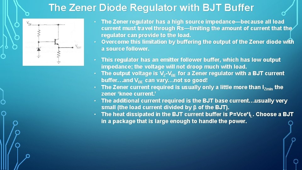
The Zener Diode Regulator with BJT Buffer • The Zener regulator has a high source impedance—because all load current must travel through Rs—limiting the amount of current that the regulator can provide to the load. • Overcome this limitation by buffering the output of the Zener diode with a source follower. • This regulator has an emitter follower buffer, which has low output impedance; the voltage will not droop much with load. • The output voltage is VZ-VBE for a Zener regulator with a BJT current buffer…and VBE can vary…not so good! • The Zener current required is usually only a little more than IZmin the zener ‘knee current. ’ • The additional current required is the BJT base current…usually very small (the load current divided by β of the BJT). • The heat dissipated in the BJT current buffer is P=Vce*IL. Choose a BJT in a package that is large enough to handle the power.

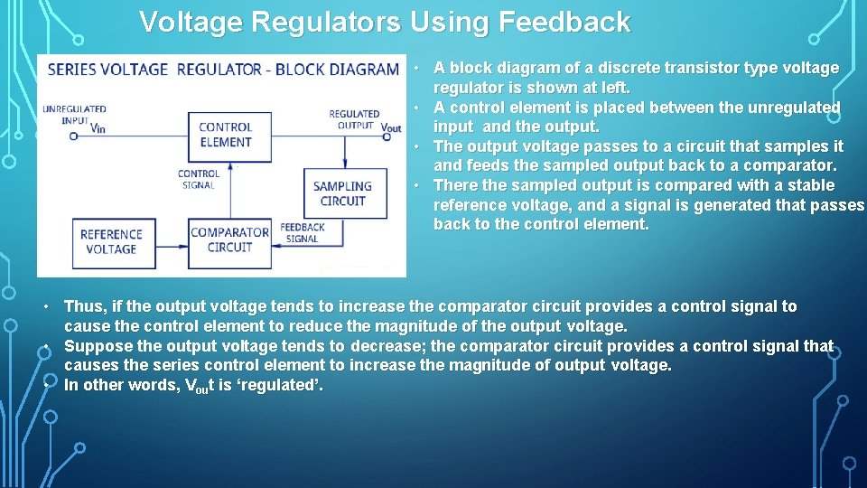
Voltage Regulators Using Feedback • A block diagram of a discrete transistor type voltage regulator is shown at left. • A control element is placed between the unregulated input and the output. • The output voltage passes to a circuit that samples it and feeds the sampled output back to a comparator. • There the sampled output is compared with a stable reference voltage, and a signal is generated that passes back to the control element. • Thus, if the output voltage tends to increase the comparator circuit provides a control signal to cause the control element to reduce the magnitude of the output voltage. • Suppose the output voltage tends to decrease; the comparator circuit provides a control signal that causes the series control element to increase the magnitude of output voltage. • In other words, Vout is ‘regulated’.

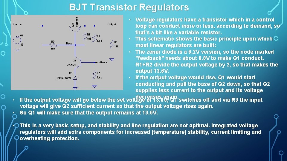
BJT Transistor Regulators • Voltage regulators have a transistor which in a control loop can conduct more or less, according to demand, so that's a bit like a variable resistor. • This schematic shows the basic principle upon which most linear regulators are built: • The zener diode is a 6. 2 V version, so the node marked "feedback" needs about 6. 8 V to make Q 1 conduct. R 1+R 2 divide the output voltage by 2, so that makes the output 13. 6 V. • If the output voltage would rise, Q 1 would start conducting and pull the base of Q 2 down, so that Q 2 supplies less current to the output and its voltage decreases again. • If the output voltage will go below the set voltage of 13. 6 V, Q 1 switches off and via R 3 the input voltage will give Q 2 sufficient current so that the output voltage rises again. • So Q 1 will make sure that the output remains at 13. 6 V. • This is a very basic setup, and stability and line regulation are not optimal. Integrated voltage regulators will add extra components for increased (temperature) stability, current limiting and overheating protection.

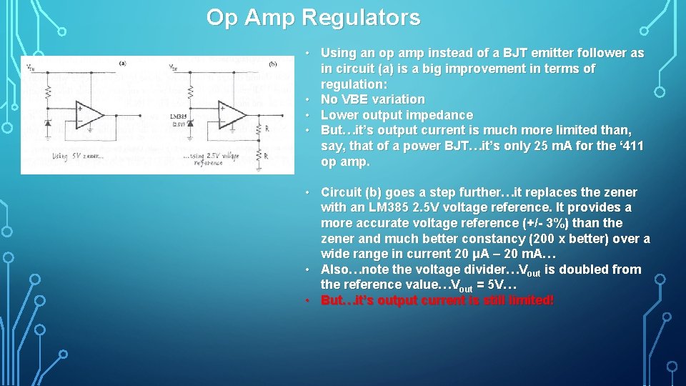
Op Amp Regulators • Using an op amp instead of a BJT emitter follower as in circuit (a) is a big improvement in terms of regulation: • No VBE variation • Lower output impedance • But…it’s output current is much more limited than, say, that of a power BJT…it’s only 25 m. A for the ‘ 411 op amp. • Circuit (b) goes a step further…it replaces the zener with an LM 385 2. 5 V voltage reference. It provides a more accurate voltage reference (+/- 3%) than the zener and much better constancy (200 x better) over a wide range in current 20 μA – 20 m. A… • Also…note the voltage divider…Vout is doubled from the reference value…Vout = 5 V… • But…it’s output current is still limited!

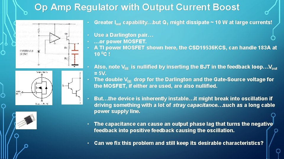
Op Amp Regulator with Output Current Boost • Greater Iout capability…but Q 1 might dissipate ~ 10 W at large currents! • Use a Darlington pair… • …or power MOSFET. • A TI power MOSFET shown here, the CSD 19536 KCS, can handle 183 A at 10 0 C ! • Also, note VBE is nullified by inserting the BJT in the feedback loop…V out = 5 V. • The double VBE drop for the Darlington and the Gate-Source voltage for the MOSFET, if either are used, are also nullified. • But…the device is inherently instable…it might break into oscillation if driving something with a lot of stray capacitance…such as a long cable power supply line. • The capacitance can cause an output phase lag that turns the negative feedback into positive feedback causing the oscillation. • Can we fix this problem and still keep its desirable characteristics?

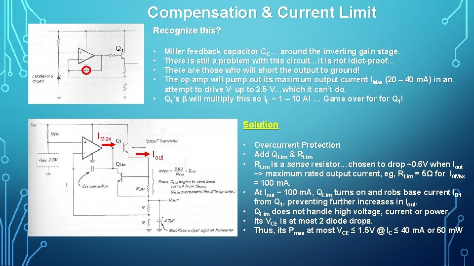
Compensation & Current Limit Recognize this? Q 1 • • • Miller feedback capacitor CC… around the inverting gain stage. There is still a problem with this circuit…it is not idiot-proof… There are those who will short the output to ground! The op amp will pump out its maximum output current I Max (20 – 40 m. A) in an attempt to drive V- up to 2. 5 V…which it can’t do. Q 1’s β will multiply this so IE ~ 1 – 10 A! … Game over for Q 1! Solution IMax Iout • Overcurrent Protection • Add QLim & RLim • RLim is a sense resistor…chosen to drop ~0. 6 V when Iout ~> maximum rated output current, eg, RLim = 5Ω for I 0 Max = 100 m. A. • At Iout ~ 100 m. A, QLim turns on and robs base current IB 1 from Q 1, preventing further increases in Iout. • QLim does not handle high voltage, current or power. • Its VCE is at most 2 diode drops. • Thus, its Pmax at most VCE ≤ 1. 5 V @ IC ≤ 40 m. A or 60 m. W

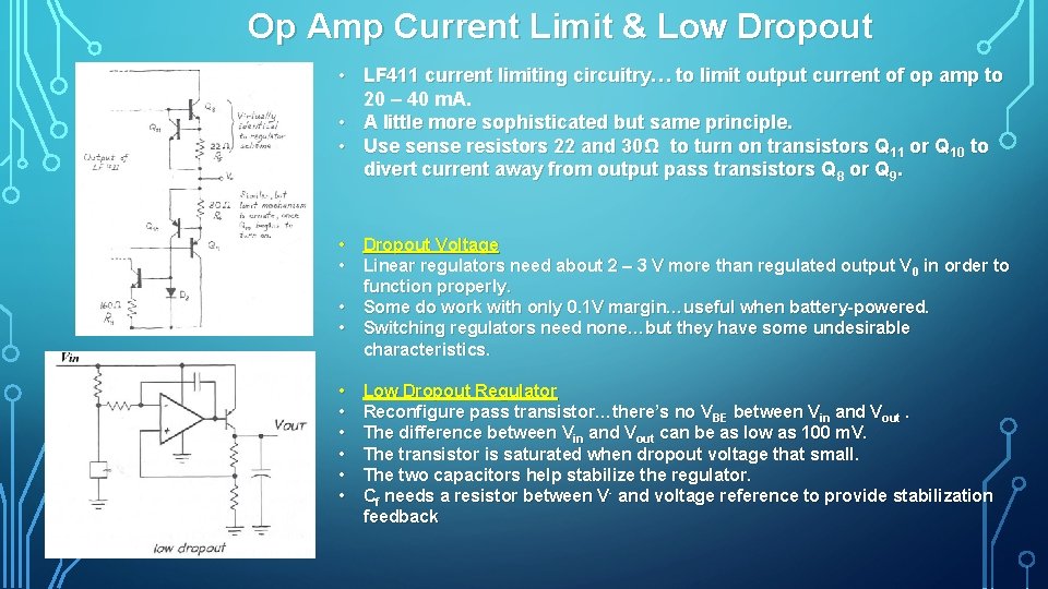
Op Amp Current Limit & Low Dropout • LF 411 current limiting circuitry… to limit output current of op amp to 20 – 40 m. A. • A little more sophisticated but same principle. • Use sense resistors 22 and 30Ω to turn on transistors Q 11 or Q 10 to divert current away from output pass transistors Q 8 or Q 9. • Dropout Voltage • Linear regulators need about 2 – 3 V more than regulated output V 0 in order to function properly. • Some do work with only 0. 1 V margin…useful when battery-powered. • Switching regulators need none…but they have some undesirable characteristics. • • • Low Dropout Regulator Reconfigure pass transistor…there’s no VBE between Vin and Vout. The difference between Vin and Vout can be as low as 100 m. V. The transistor is saturated when dropout voltage that small. The two capacitors help stabilize the regulator. Cf needs a resistor between V- and voltage reference to provide stabilization feedback

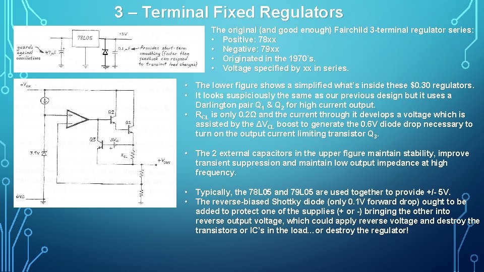
3 – Terminal Fixed Regulators The original (and good enough) Fairchild 3 -terminal regulator series: • Positive: 78 xx • Negative: 79 xx • Originated in the 1970’s. • Voltage specified by xx in series. • The lower figure shows a simplified what’s inside these $0. 30 regulators. • It looks suspiciously the same as our previous design but it uses a Darlington pair Q 1 & Q 2 for high current output. • RCL is only 0. 2Ω and the current through it develops a voltage which is assisted by the ΔVCL boost to generate the 0. 6 V diode drop necessary to turn on the output current limiting transistor Q 3. • The 2 external capacitors in the upper figure maintain stability, improve transient suppression and maintain low output impedance at high frequency. • Typically, the 78 L 05 and 79 L 05 are used together to provide +/- 5 V. • The reverse-biased Shottky diode (only 0. 1 V forward drop) ought to be added to protect one of the supplies (+ or -) bringing the other into reverse output voltage, which could apply reverse voltage and destroy the transistors or IC’s in the load…or destroy the regulator!

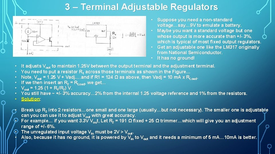
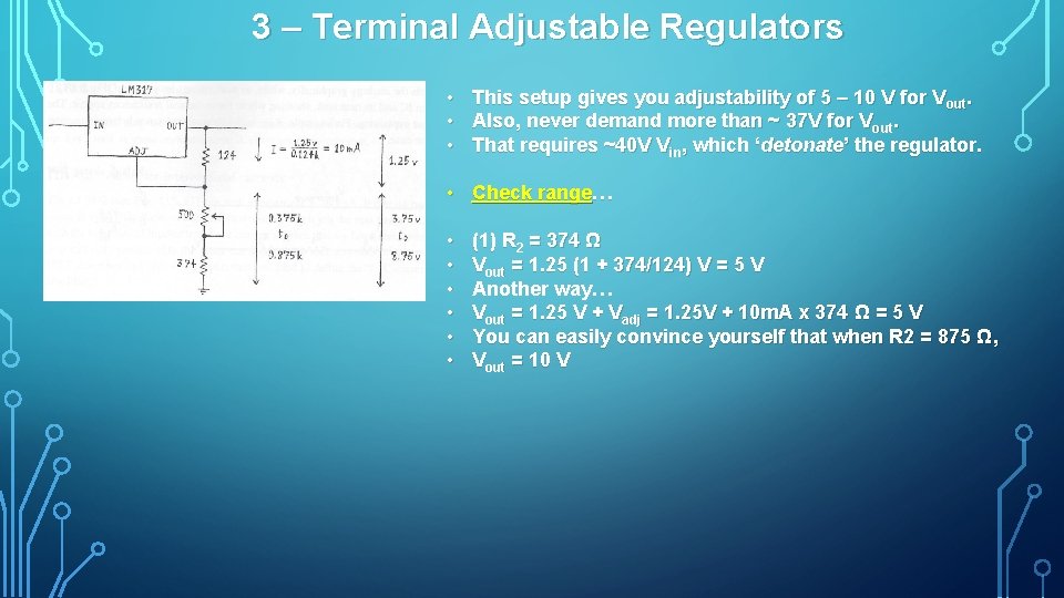
3 – Terminal Adjustable Regulators R 1 • • Suppose you need a non-standard voltage…say… 9 V to emulate a battery. • Maybe you want a standard voltage but one whose output is more accurate than +/- 3%, which is typical of most fixed output regulators. • Get an adjustable one like the LM 317 originally from National Semiconductor. • It has no ground! It adjusts Vout to maintain 1. 25 V between the output terminal and the adjustment terminal. You need to put a resistor R 1 across those terminals as shown in the Figure… Note, Vout = 1. 25 V + Vadj…. and if R 1 = 124 Ω as above, then Vadj = 10 m. A x RLoad. If we then insert an R 2 = RLoad, we get… Vout = 1. 25 (1 + R 1/R 2) V. You still have ~ +/- 3% accuracy… 2% from the internal 1. 25 voltage reference and 1% from the resistors. Solution: • Break up R 2 into 2 resistors…one small and one large (usually…but not necessary). The smaller one is adjustable can you can use it to adjust Vout with great accuracy. • For example… if you want 3. 3 V Vout, Let R 2 = 191 Ω fixed + 25 Ω trimmer…which will give you an adjustment range of +/- 6%. • The unregulated input voltage Vin must be 2 V > Vout. • Also, because it has no ground, it is powered by Vin to Vout and it needs a minimum of 5 m. A… 10 m. A is better.

3 – Terminal Adjustable Regulators • • • This setup gives you adjustability of 5 – 10 V for Vout. Also, never demand more than ~ 37 V for Vout. That requires ~40 V Vin, which ‘detonate’ the regulator. • Check range… • • • (1) R 2 = 374 Ω Vout = 1. 25 (1 + 374/124) V = 5 V Another way… Vout = 1. 25 V + Vadj = 1. 25 V + 10 m. A x 374 Ω = 5 V You can easily convince yourself that when R 2 = 875 Ω, Vout = 10 V

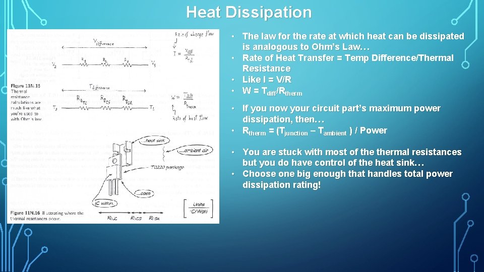
Heat Dissipation • The law for the rate at which heat can be dissipated is analogous to Ohm’s Law… • Rate of Heat Transfer = Temp Difference/Thermal Resistance • Like I = V/R • W = Tdiff/Rtherm • If you now your circuit part’s maximum power dissipation, then… • Rtherm = (Tjunction – Tambient ) / Power • You are stuck with most of thermal resistances but you do have control of the heat sink… • Choose one big enough that handles total power dissipation rating!

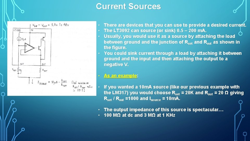
Current Sources • • • There are devices that you can use to provide a desired current. The LT 3092 can source (or sink) 0. 5 – 200 m. A. Usually, you would use it as a source by attaching the load between ground and the junction of Rset and Rout as shown in the figure. • You could sink current through a load by attaching it between ground and the input and then attaching the output to a negative V. • As an example: • If you wanted a 10 m. A source (like our previous example with the LM 317) you would choose Rset = 20 K and Rout = 20 Ω giving Rset / Rout =1000 and Isource = 10 m. A. • The output impedance of this source is spectacular… • 100 MΩ at dc and 3 MΩ at 1 KHz

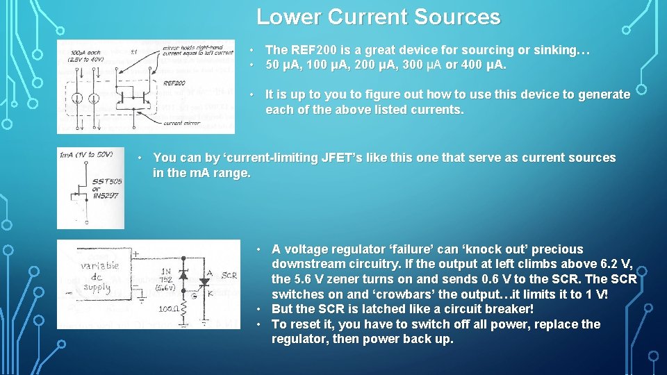
Lower Current Sources • The REF 200 is a great device for sourcing or sinking… • 50 μA, 100 μA, 200 μA, 300 μA or 400 μA. • It is up to you to figure out how to use this device to generate each of the above listed currents. • You can by ‘current-limiting JFET’s like this one that serve as current sources in the m. A range. • A voltage regulator ‘failure’ can ‘knock out’ precious downstream circuitry. If the output at left climbs above 6. 2 V, the 5. 6 V zener turns on and sends 0. 6 V to the SCR. The SCR switches on and ‘crowbars’ the output…it limits it to 1 V! • But the SCR is latched like a circuit breaker! • To reset it, you have to switch off all power, replace the regulator, then power back up.

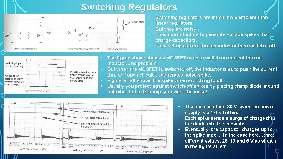
Switching Regulators • Switching regulators are much more efficient than linear regulators. • But they are noisy… • They use inductors to generate voltage spikes that charge capacitors. • They set up current thru an inductor then switch it off. • The figure above shows a MOSFET used to switch on current thru an inductor…no problem. • But when the MOSFET is switched off, the inductor tries to push the current thru an “open circuit”…generates noise spike. • Figure at left shows the spike when switching to off. • Usually you protect against switch-off spikes by placing clamp diode around inductor, but in this app, you want the spike! • The spike is about 80 V, even tho power supply is a 1. 6 V battery! • Each spike sends a surge of charge thru the diode into the capacitor. • Eventually, the capacitor charges up to the spike max … in the case here…three different values, 25, 10 and 5 V as shown in the figure at left.

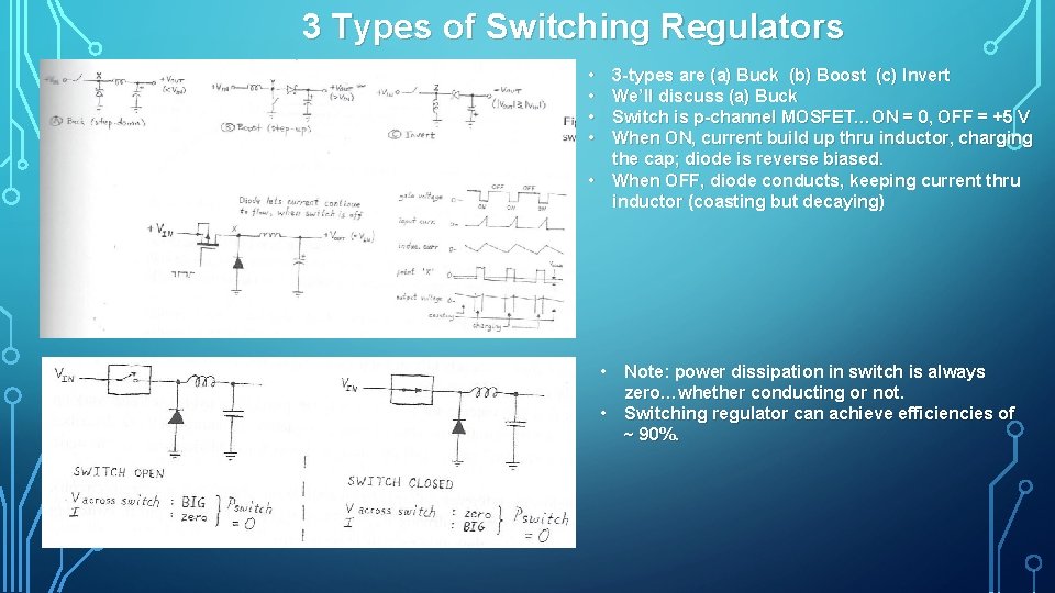
3 Types of Switching Regulators • • • 3 -types are (a) Buck (b) Boost (c) Invert We’ll discuss (a) Buck Switch is p-channel MOSFET…ON = 0, OFF = +5 V When ON, current build up thru inductor, charging the cap; diode is reverse biased. When OFF, diode conducts, keeping current thru inductor (coasting but decaying) • Note: power dissipation in switch is always zero…whether conducting or not. • Switching regulator can achieve efficiencies of ~ 90%.

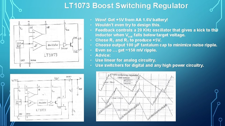
LT 1073 Boost Switching Regulator • • • Wow! Get +5 V from AA 1. 6 V battery! Wouldn’t even try to design this. Feedback controls a 20 KHz oscillator that gives a kick to the inductor when Vout falls below target voltage. Chose R 1 and R 2 to produce +5 V. Choose output 100 μF tantalum cap to minimize noise ripple. Even so … get ~150 m. V ripple. Advice: Use linear for analog circuitry. Use switchers for digital and any high power circuitry.