
ECE 4211 L 12 FETs Gate Sizing FET


- Slides: 32
ECE 4211 L 12 FETs, Gate Sizing, FET Scaling 04112017 F. Jain 8. 7 MOSFETs 8. 7. 1 Voltage-Current Equation of a n-channel Al-Si. O 2 -p. Si Device 572 8. 7. 2 Various Regions of ID - VD Characteristics 575 8. 7. 3 MOSFET Summary 8. 7. 4 Solved Problem Set Chapter 9: Short channel effects and FET Scaling Laws p. 606 -612: Slide 25+ 571 579 582 Chapter 10: FET Scaling p. 606 -612: Slides FET SIZING for NMOS Inverters and Logic Gates Inverters using driver and load transistors Inverter threshold VINV(not FET threshold VTH) Propagation delay in NMOS CMOS Operation CMOS Inverter sizing: W/L ratio of NMOS and PMOS Propagation Delay in CMOS inverters 1
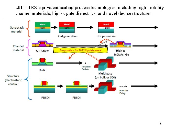
. 2011 ITRS equivalent scaling process technologies, including high mobility channel materials, high-k gate dielectrics, and novel device structures 2
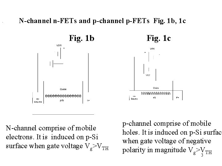
. N-channel n-FETs and p-channel p-FETs Fig. 1 b, 1 c Fig. 1 b N-channel comprise of mobile electrons. It is induced on p-Si surface when gate voltage Vg>VTH Fig. 1 c p-channel comprise of mobile holes. It is induced on p-Si surface when gate voltage of negative polarity in magnitude Vg>VTH 3
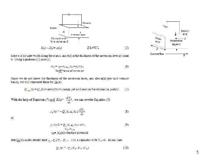
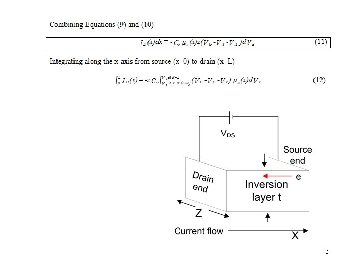
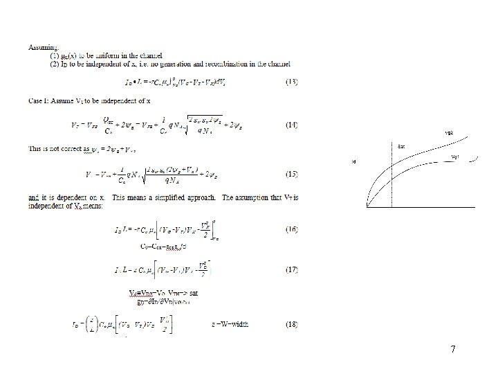
8. 5. 1 Voltage-Current Equation of a n-channel Al-Si. O 2 -p. Si N-channel FET, Fig. 1(A) page 572 The work function difference increases as ND is increased. 4
5
6
7
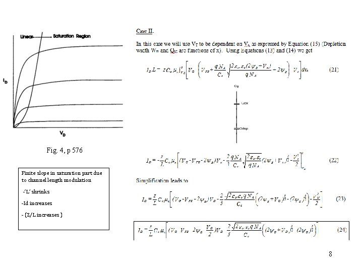
Fig. 4, p 576 Finite slope in saturation part due to channel length modulation -‘L’ shrinks -Id increases - (Z/L increases ) 8
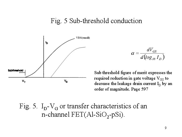
Fig. 5 Sub-threshold conduction Sub threshold figure of merit expresses the required reduction in gate voltage VGS to decrease the leakage drain current ID by an order of magnitude. Page 597 Fig. 5. ID-VG or transfer characteristics of an n-channel FET(Al-Si. O 2 -p. Si). 9
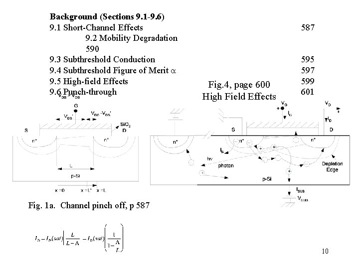
Background (Sections 9. 1 -9. 6) 9. 1 Short-Channel Effects 9. 2 Mobility Degradation 590 9. 3 Subthreshold Conduction 9. 4 Subthreshold Figure of Merit 9. 5 High-field Effects 9. 6 Punch-through 587 Fig. 4, page 600 High Field Effects 595 597 599 601 Fig. 1 a. Channel pinch off, p 587 10
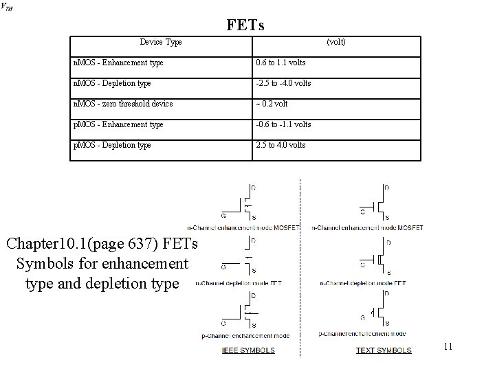
FETs Device Type (volt) n. MOS - Enhancement type 0. 6 to 1. 1 volts n. MOS - Depletion type -2. 5 to -4. 0 volts n. MOS - zero threshold device ~ 0. 2 volt p. MOS - Enhancement type -0. 6 to -1. 1 volts p. MOS - Depletion type 2. 5 to 4. 0 volts Chapter 10. 1(page 637) FETs Symbols for enhancement type and depletion type 11
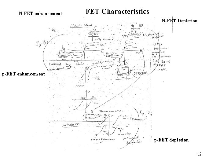
N-FET enhancement FET Characteristics N-FET Depletion p-FET enhancement p-FET depletion 12
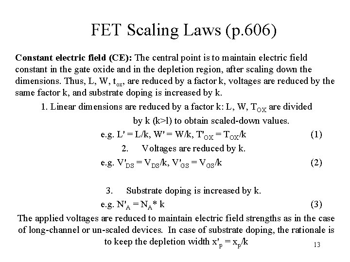
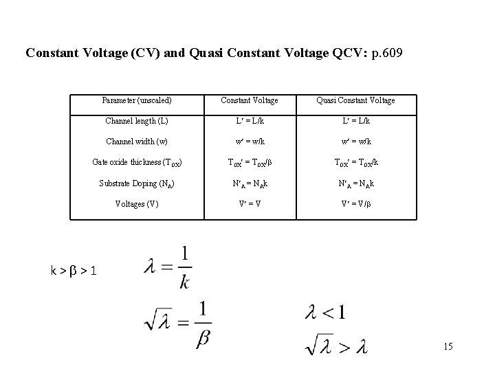
FET Scaling Laws (p. 606) Constant electric field (CE): The central point is to maintain electric field constant in the gate oxide and in the depletion region, after scaling down the dimensions. Thus, L, W, tox, are reduced by a factor k, voltages are reduced by the same factor k, and substrate doping is increased by k. 1. Linear dimensions are reduced by a factor k: L, W, TOX are divided by k (k>l) to obtain scaled-down values. e. g. L' = L/k, W' = W/k, T'OX = TOX/k (1) 2. Voltages are reduced by k. e. g. V'DS = VDS/k, V'GS = VGS/k (2) 3. Substrate doping is increased by k. e. g. N'A = NA* k (3) The applied voltages are reduced to maintain electric field strengths as in the case of long-channel or un-scaled devices. In case of substrate doping, the rationale is to keep the depletion width x'p = xp/k 13
CE Scaling and Power-delay product Parameter Unscaled Scaled Value Capacitance (total; F) c. OXw. L w L c OX = c. OXw. L/k Charge (Total, coulomb) Qw. L Q w L = Qw. L/k 2 Capacitance per unit area c. OX c OX = c. OX*k Charge per unit area Q Q = Q Power Dissipation (VI) P p = p/k 2 Power Density (VI/w. L) (p /w L ) = (p/w. L) Delay Time (w. LQ/I) = /k Resistance R R = Rk 14
Constant Voltage (CV) and Quasi Constant Voltage QCV: p. 609 Parameter (unscaled) Constant Voltage Quasi Constant Voltage Channel length (L) L = L/k Channel width (w) w = w/k Gate oxide thickness (T OX) TOX = TOX/k Substrate Doping (NA) N A = NAk Voltages (V) V = V/ k> >1 15
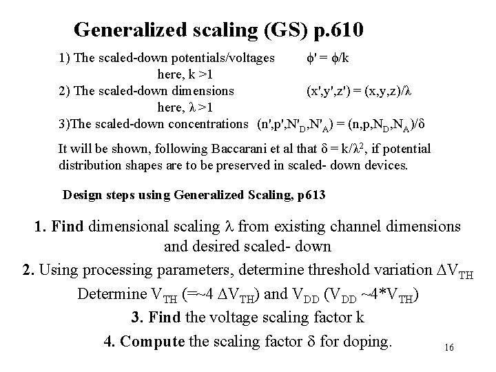
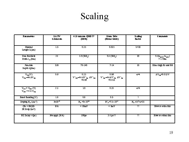
Generalized scaling (GS) p. 610 1) The scaled-down potentials/voltages ϕ' = ϕ/k here, k >1 2) The scaled-down dimensions (x', y', z') = (x, y, z)/λ here, λ >1 3)The scaled-down concentrations (n', p', N'D, N'A) = (n, p, ND, NA)/δ It will be shown, following Baccarani et al that δ = k/λ 2, if potential distribution shapes are to be preserved in scaled- down devices. Design steps using Generalized Scaling, p 613 1. Find dimensional scaling from existing channel dimensions and desired scaled- down 2. Using processing parameters, determine threshold variation DVTH Determine VTH (=~4 DVTH) and VDD (VDD ~4*VTH) 3. Find the voltage scaling factor k 4. Compute the scaling factor d for doping. 16
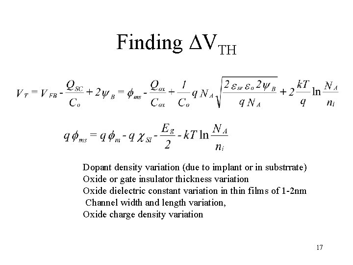
Finding DVTH Dopant density variation (due to implant or in substrrate) Oxide or gate insulator thickness variation Oxide dielectric constant variation in thin films of 1 -2 nm Channel width and length variation, Oxide charge density variation 17
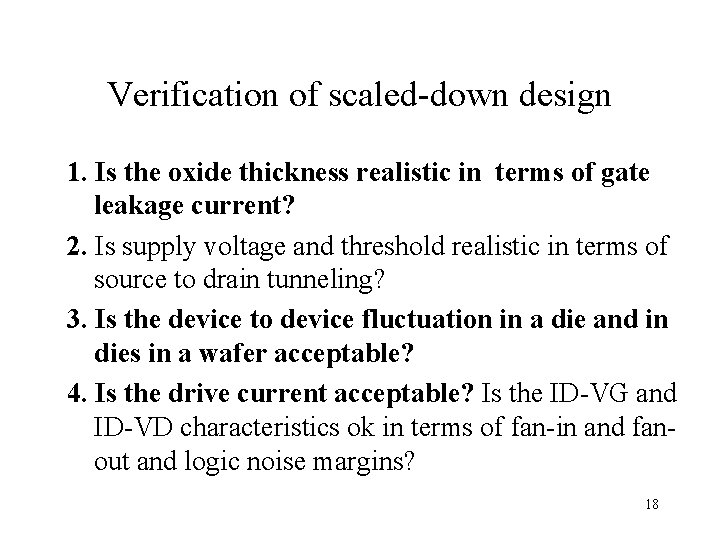
Verification of scaled-down design 1. Is the oxide thickness realistic in terms of gate leakage current? 2. Is supply voltage and threshold realistic in terms of source to drain tunneling? 3. Is the device to device fluctuation in a die and in dies in a wafer acceptable? 4. Is the drive current acceptable? Is the ID-VG and ID-VD characteristics ok in terms of fan-in and fanout and logic noise margins? 18
Scaling Parameters LATV 1. 3 micron 0. 25 micron QMDT* (IBM) 25 nm Si. Ge (Home work) Scaling factor Comments Channel Length L( m) 1. 3 0. 25 0. 025 =10 Gate Insulator Oxide tox (nm) 25 5. 0 (Si. O 2) 0. 5 (Si. O 2) 10 0. 5(e. Hf. O 2 /e. Si. O 2) = 1. 7 nm Junction Depth xj(nm) 350 70 -140 7 -14 10 Gives high Rs and Rd VTH (V) VTH =4 x DVTH 0. 6 0. 25 V’TH =4 x DV’TH =0. 06 V’TH =4 x DV’TH =0. 015 =4 DVTH=0. 015 V VDS = VDD (V) VDD = 4 x VTH 2. 5 1. 0 0. 25 =4 Band Bending (V) 1. 8 0. 3 ? Doping NA (cm-3) 3 x 10¹⁵ NA =3 1016 N’A=7. 5 1017 NA x 2/ =25 (Rs + Rd)ID IR Drop (m. V) NA < 10 m. V < 1 m. V ? ? How to solve this RC Delay (ps) Not appl. (NA) 100 ps 2 -5 ps? ? How to solver this 19
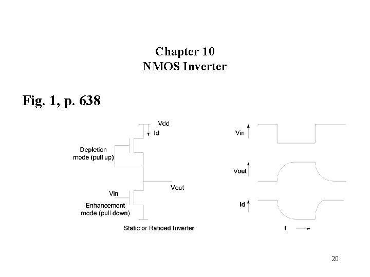
Chapter 10 NMOS Inverter Fig. 1, p. 638 20
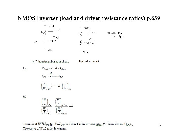
NMOS Inverter (load and driver resistance ratios) p. 639 21
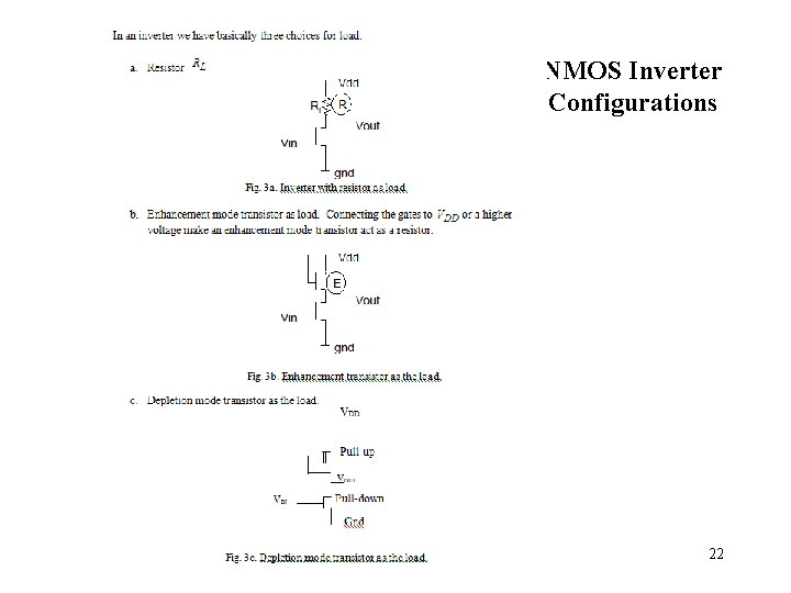
NMOS Inverter Configurations 22
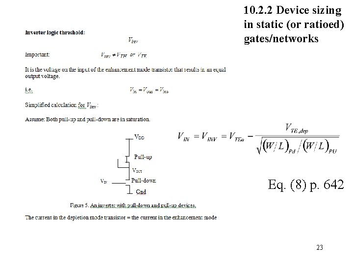
10. 2. 2 Device sizing in static (or ratioed) gates/networks Eq. (8) p. 642 23
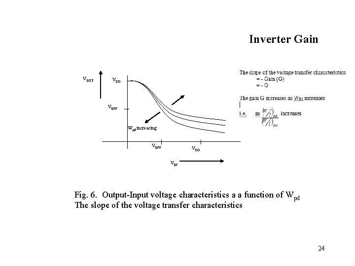
Inverter Gain VOUT VDD VINV Wpd increasing VINV VDD VIN Fig. 6. Output-Input voltage characteristics a a function of Wpd The slope of the voltage transfer characteristics 24
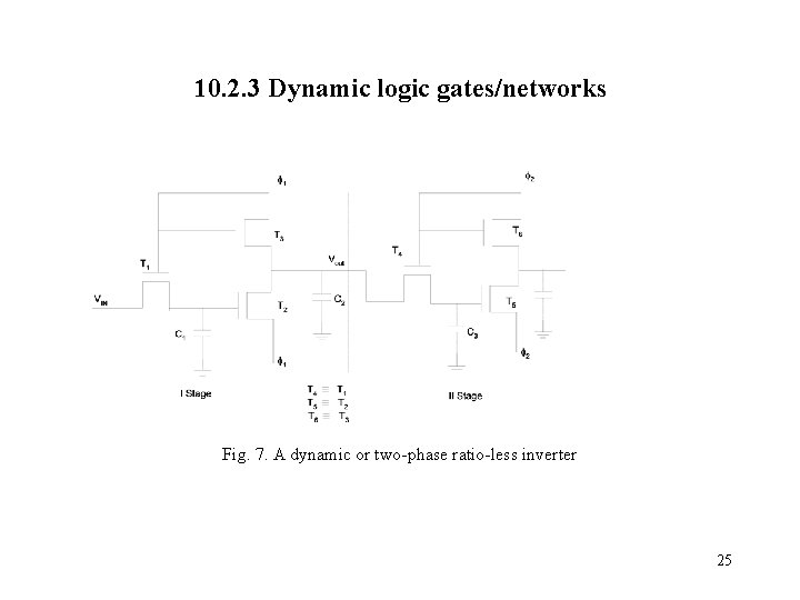
10. 2. 3 Dynamic logic gates/networks Fig. 7. A dynamic or two-phase ratio-less inverter 25
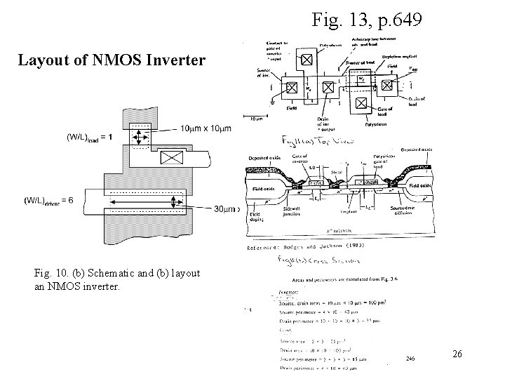
Fig. 13, p. 649 Layout of NMOS Inverter Fig. 10. (b) Schematic and (b) layout an NMOS inverter. 26
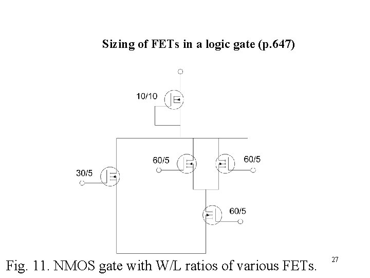
Sizing of FETs in a logic gate (p. 647) Fig. 11. NMOS gate with W/L ratios of various FETs. 27
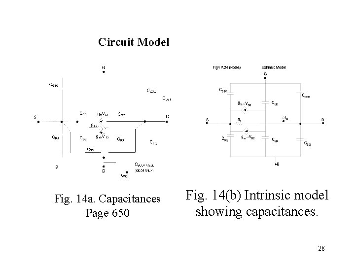
Circuit Model Fig. 14 a. Capacitances Page 650 Fig. 14(b) Intrinsic model showing capacitances. 28
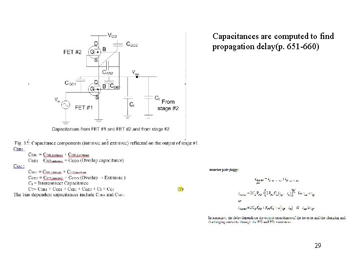
Capacitances are computed to find propagation delay(p. 651 -660) 29
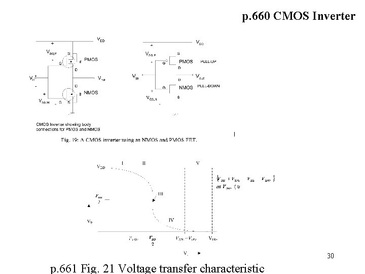
p. 660 CMOS Inverter 30 p. 661 Fig. 21 Voltage transfer characteristic
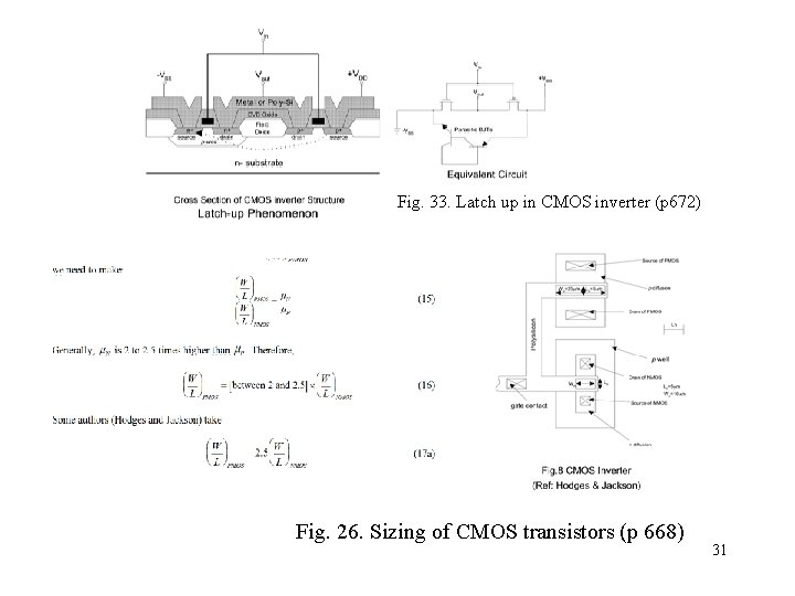
Fig. 33. Latch up in CMOS inverter (p 672) Fig. 26. Sizing of CMOS transistors (p 668) 31
Fig. 27 Sizing of 2 -input NOR 2 -input NAND CMOS inverter (p 668) 32