Wires 6 884 Spring 2005 21105 L 04
- Slides: 26

Wires 6. 884 – Spring 2005 2/11/05 L 04 – Wires 1

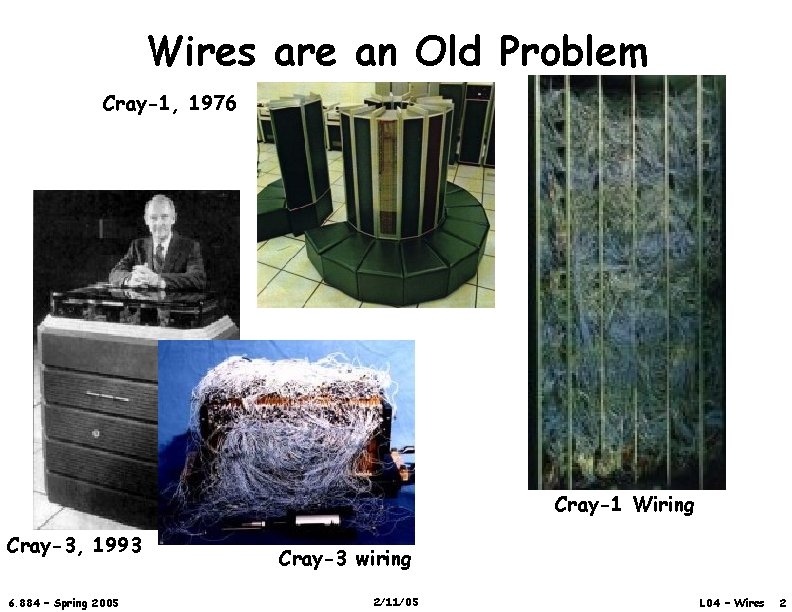
Wires are an Old Problem Cray-1, 1976 Cray-1 Wiring Cray-3, 1993 6. 884 – Spring 2005 Cray-3 wiring 2/11/05 L 04 – Wires 2

Interconnect Problems § A lot of circuit designers are very worried about what’s happening with wires in CMOS technology § Device technology has been scaling well, with gate performance increasing linearly with decreasing feature size § Wires scale differently, and long wires have been getting relatively slower over time § Wire delay is a function of wire resistance and capacitance 6. 884 – Spring 2005 2/11/05 L 04 – Wires 3

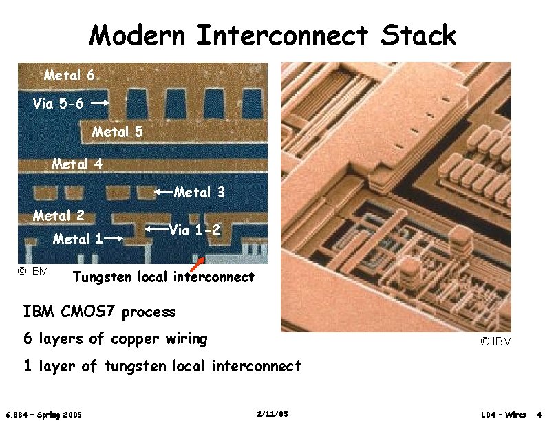
Modern Interconnect Stack Metal 6 Via 5 -6 Metal 5 Metal 4 Metal 3 Metal 2 Metal 1 © IBM Via 1 -2 Tungsten local interconnect IBM CMOS 7 process 6 layers of copper wiring © IBM 1 layer of tungsten local interconnect 6. 884 – Spring 2005 2/11/05 L 04 – Wires 4

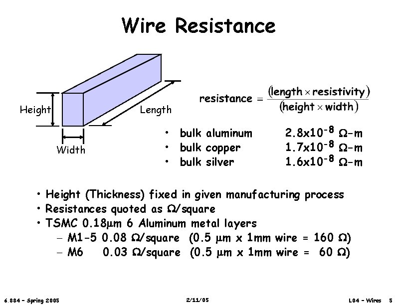
Wire Resistance Height Length Width • bulk aluminum • bulk copper • bulk silver 2. 8 x 10 -8 -m 1. 7 x 10 -8 -m 1. 6 x 10 -8 -m • Height (Thickness) fixed in given manufacturing process • Resistances quoted as /square • TSMC 0. 18 mm 6 Aluminum metal layers – M 1 -5 0. 08 /square (0. 5 mm x 1 mm wire = 160 ) – M 6 0. 03 /square (0. 5 mm x 1 mm wire = 60 ) 6. 884 – Spring 2005 2/11/05 L 04 – Wires 5

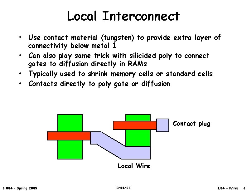
Local Interconnect • Use contact material (tungsten) to provide extra layer of connectivity below metal 1 • Can also play same trick with silicided poly to connect gates to diffusion directly in RAMs • Typically used to shrink memory cells or standard cells • Contacts directly to poly gate or diffusion Contact plug Local Wire 6. 884 – Spring 2005 2/11/05 L 04 – Wires 6

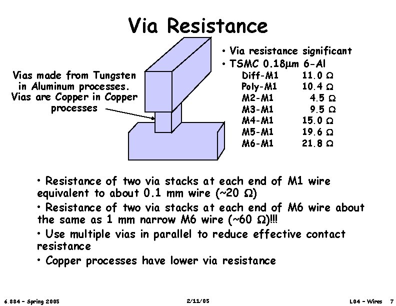
Via Resistance • Via resistance significant • TSMC 0. 18 mm 6 -Al Vias made from Tungsten in Aluminum processes. Vias are Copper in Copper processes Diff-M 1 Poly-M 1 M 2 -M 1 M 3 -M 1 M 4 -M 1 M 5 -M 1 M 6 -M 1 11. 0 10. 4 4. 5 9. 5 15. 0 19. 6 21. 8 • Resistance of two via stacks at each end of M 1 wire equivalent to about 0. 1 mm wire (~20 ) • Resistance of two via stacks at each end of M 6 wire about the same as 1 mm narrow M 6 wire (~60 )!!! • Use multiple vias in parallel to reduce effective contact resistance • Copper processes have lower via resistance 6. 884 – Spring 2005 2/11/05 L 04 – Wires 7

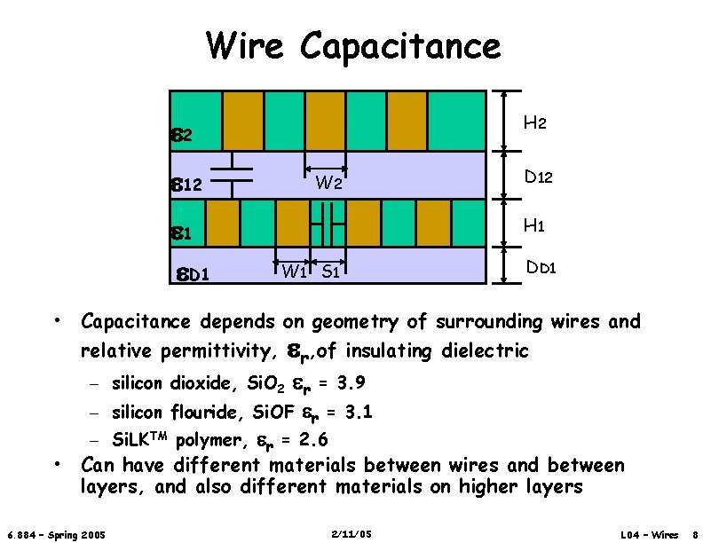
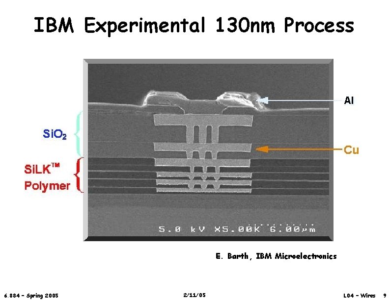
Wire Capacitance H 2 2 12 W 2 1 D 12 H 1 W 1 S 1 DD 1 • Capacitance depends on geometry of surrounding wires and relative permittivity, r, of insulating dielectric – silicon dioxide, Si. O 2 r = 3. 9 – silicon flouride, Si. OF r = 3. 1 – Si. LKTM polymer, r = 2. 6 • Can have different materials between wires and between layers, and also different materials on higher layers 6. 884 – Spring 2005 2/11/05 L 04 – Wires 8

IBM Experimental 130 nm Process Al E. Barth, IBM Microelectronics 6. 884 – Spring 2005 2/11/05 L 04 – Wires 9

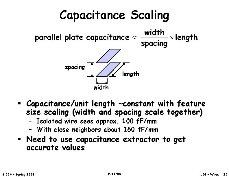
Capacitance Scaling spacing length width § Capacitance/unit length ~constant with feature size scaling (width and spacing scale together) – Isolated wire sees approx. 100 f. F/mm – With close neighbors about 160 f. F/mm § Need to use capacitance extractor to get accurate values 6. 884 – Spring 2005 2/11/05 L 04 – Wires 10

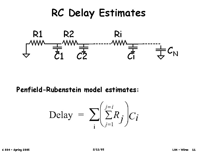
RC Delay Estimates R 1 R 2 C 1 Ri C 2 Ci CN Penfield-Rubenstein model estimates: 6. 884 – Spring 2005 2/11/05 L 04 – Wires 11

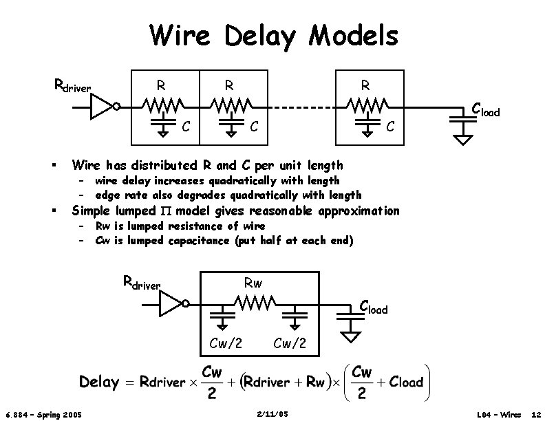
Wire Delay Models Rdriver R R C § § R C C Cload Wire has distributed R and C per unit length – – wire delay increases quadratically with length edge rate also degrades quadratically with length – – Rw is lumped resistance of wire Cw is lumped capacitance (put half at each end) Simple lumped P model gives reasonable approximation Rdriver Rw Cload Cw/2 6. 884 – Spring 2005 Cw/2 2/11/05 L 04 – Wires 12

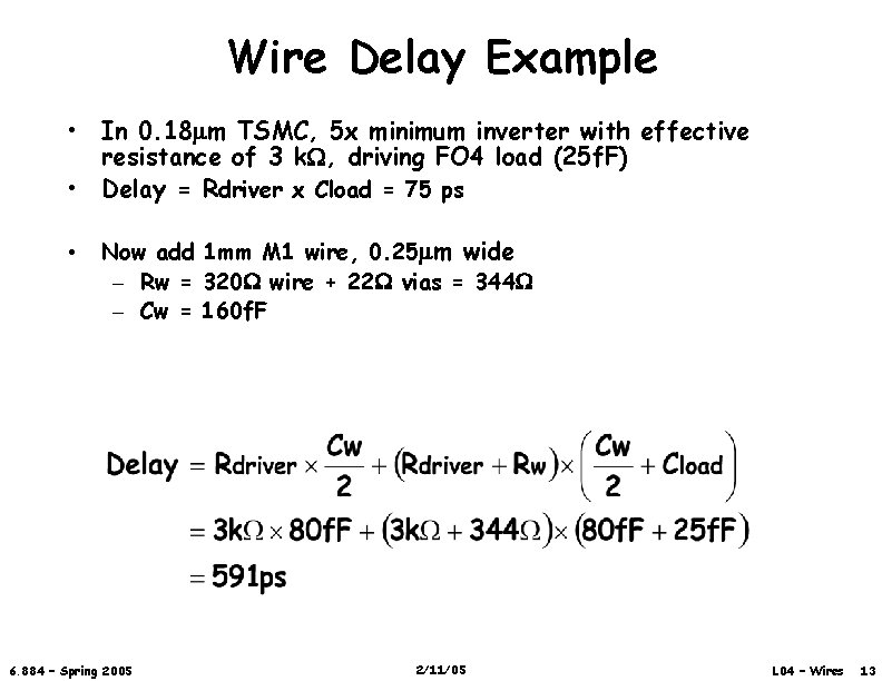
Wire Delay Example • In 0. 18 mm TSMC, 5 x minimum inverter with effective resistance of 3 k , driving FO 4 load (25 f. F) • Delay = Rdriver x Cload = 75 ps • Now add 1 mm M 1 wire, 0. 25 mm wide – Rw = 320 wire + 22 vias = 344 – Cw = 160 f. F 6. 884 – Spring 2005 2/11/05 L 04 – Wires 13

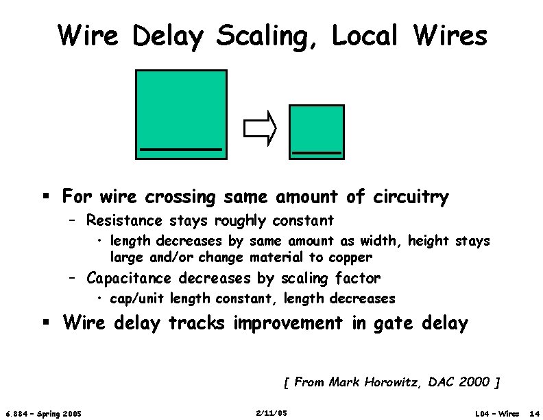
Wire Delay Scaling, Local Wires § For wire crossing same amount of circuitry – Resistance stays roughly constant • length decreases by same amount as width, height stays large and/or change material to copper – Capacitance decreases by scaling factor • cap/unit length constant, length decreases § Wire delay tracks improvement in gate delay [ From Mark Horowitz, DAC 2000 ] 6. 884 – Spring 2005 2/11/05 L 04 – Wires 14

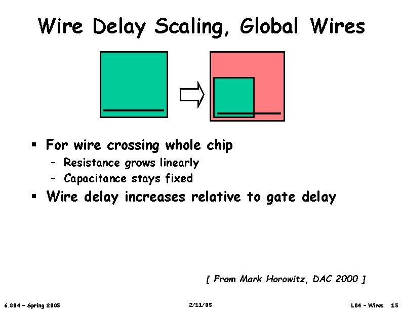
Wire Delay Scaling, Global Wires § For wire crossing whole chip – Resistance grows linearly – Capacitance stays fixed § Wire delay increases relative to gate delay [ From Mark Horowitz, DAC 2000 ] 6. 884 – Spring 2005 2/11/05 L 04 – Wires 15

Fewer Gates per Clock Cycle § Processors in Intel 386 generation, around 50 FO 4 gate delays per clock cycle § Pentium-4 around 16 FO 4 in normal clock, around 8 FO 4 delays in fast ALU section § Fastest 64 -bit adder around 7 FO 4 delays § As measured in distance per clock cycle, wires are getting much slower 6. 884 – Spring 2005 2/11/05 L 04 – Wires 16

Process Technology Fixes § Reduce R – use copper instead of aluminum, 40% reduction – provide upper layers with thicker metal for long range wires – provide more layers to improve density, makes wires shorter § Reduce C – use low-k dielectric, >2 x reduction possible – increase inter-layer spacing (limited effect, problems with via formation) – provide more layers to improve density, makes wires shorter 6. 884 – Spring 2005 2/11/05 L 04 – Wires 17

Layout Fixes § Reduce R – make wires wider, increase in C is less than increase in C because of fringing fields – use parallel vias at contacts – floorplanning to keep wires short – careful routing to avoid unnecessary layer changes (vias) § Reduce C – space wires further apart than minimum – avoid parallel wiring 6. 884 – Spring 2005 2/11/05 L 04 – Wires 18

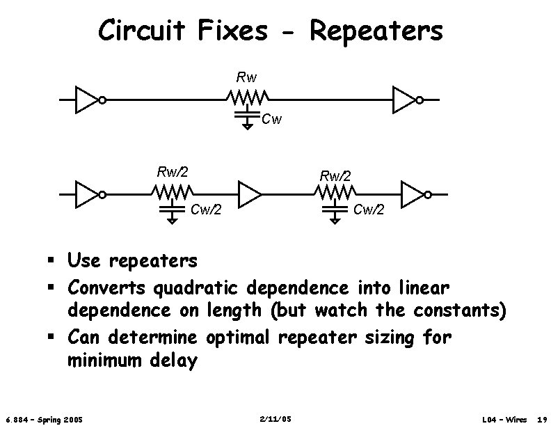
Circuit Fixes - Repeaters Rw Cw Rw/2 Cw/2 § Use repeaters § Converts quadratic dependence into linear dependence on length (but watch the constants) § Can determine optimal repeater sizing for minimum delay 6. 884 – Spring 2005 2/11/05 L 04 – Wires 19

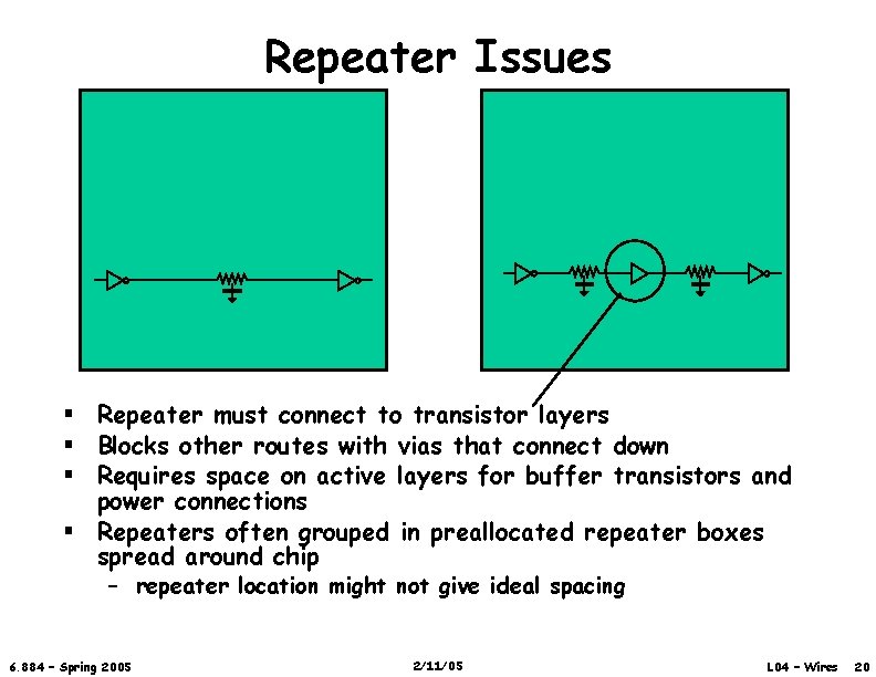
Repeater Issues § Repeater must connect to transistor layers § Blocks other routes with vias that connect down § Requires space on active layers for buffer transistors and power connections § Repeaters often grouped in preallocated repeater boxes spread around chip – repeater location might not give ideal spacing 6. 884 – Spring 2005 2/11/05 L 04 – Wires 20

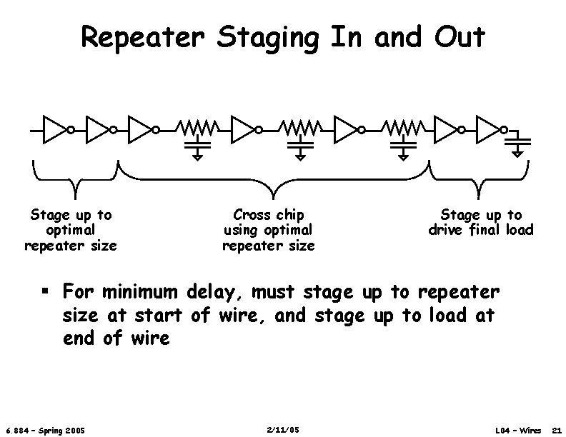
Repeater Staging In and Out Stage up to optimal repeater size Cross chip using optimal repeater size Stage up to drive final load § For minimum delay, must stage up to repeater size at start of wire, and stage up to load at end of wire 6. 884 – Spring 2005 2/11/05 L 04 – Wires 21

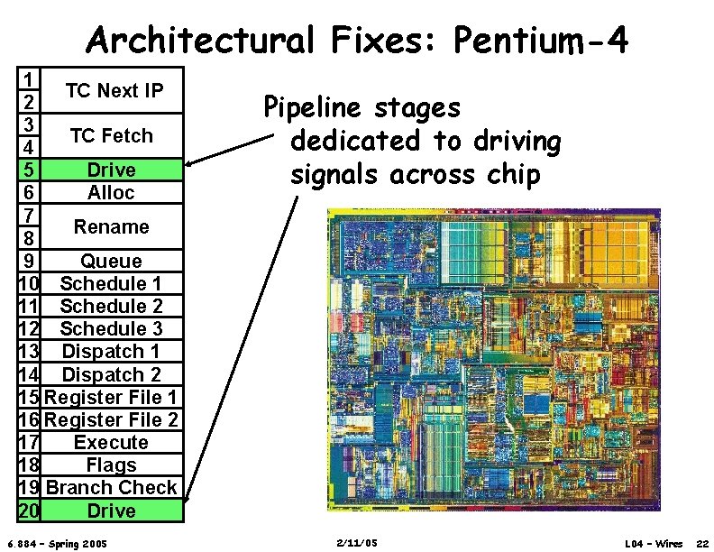
Architectural Fixes: Pentium-4 1 TC Next IP 2 3 TC Fetch 4 5 Drive 6 Alloc 7 Rename 8 9 Queue 10 Schedule 1 11 Schedule 2 12 Schedule 3 13 Dispatch 1 14 Dispatch 2 15 Register File 1 16 Register File 2 17 Execute 18 Flags 19 Branch Check 20 Drive 6. 884 – Spring 2005 Pipeline stages dedicated to driving signals across chip 2/11/05 L 04 – Wires 22

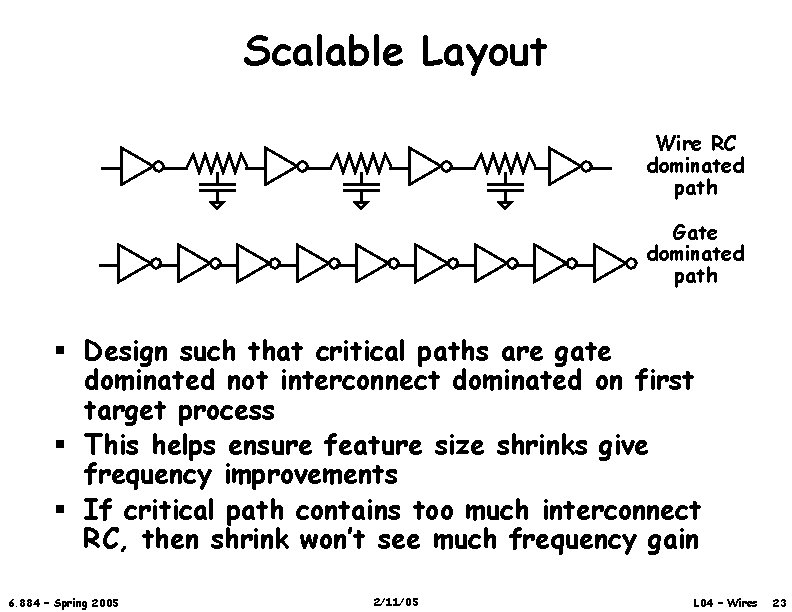
Scalable Layout Wire RC dominated path Gate dominated path § Design such that critical paths are gate dominated not interconnect dominated on first target process § This helps ensure feature size shrinks give frequency improvements § If critical path contains too much interconnect RC, then shrink won’t see much frequency gain 6. 884 – Spring 2005 2/11/05 L 04 – Wires 23

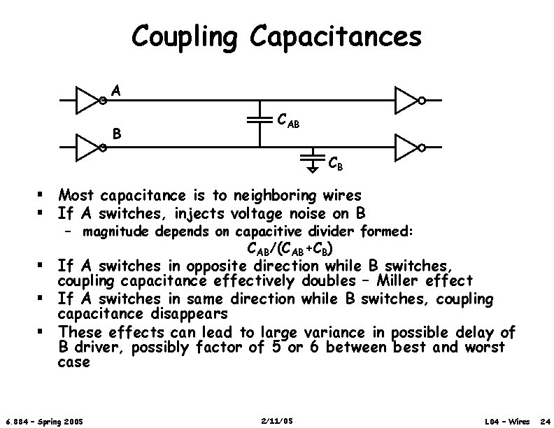
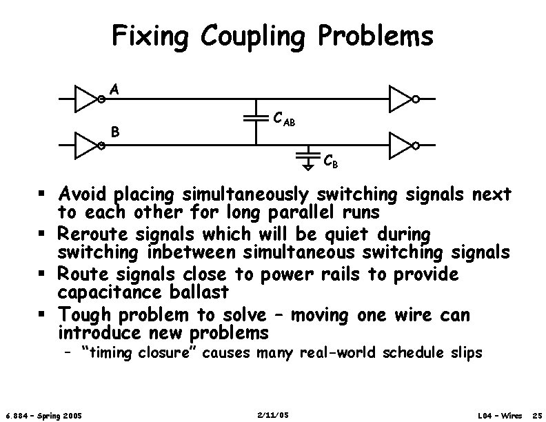
Coupling Capacitances A B CAB CB § Most capacitance is to neighboring wires § If A switches, injects voltage noise on B – magnitude depends on capacitive divider formed: CAB/(CAB+CB) § If A switches in opposite direction while B switches, coupling capacitance effectively doubles – Miller effect § If A switches in same direction while B switches, coupling capacitance disappears § These effects can lead to large variance in possible delay of B driver, possibly factor of 5 or 6 between best and worst case 6. 884 – Spring 2005 2/11/05 L 04 – Wires 24

Fixing Coupling Problems A B CAB CB § Avoid placing simultaneously switching signals next to each other for long parallel runs § Reroute signals which will be quiet during switching inbetween simultaneous switching signals § Route signals close to power rails to provide capacitance ballast § Tough problem to solve – moving one wire can introduce new problems – “timing closure” causes many real-world schedule slips 6. 884 – Spring 2005 2/11/05 L 04 – Wires 25

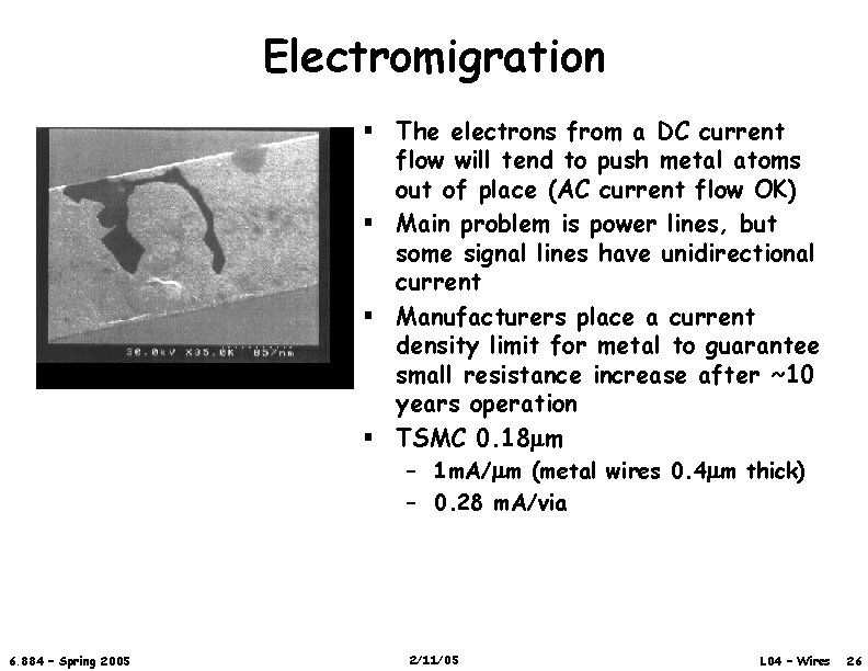
Electromigration § The electrons from a DC current flow will tend to push metal atoms out of place (AC current flow OK) § Main problem is power lines, but some signal lines have unidirectional current § Manufacturers place a current density limit for metal to guarantee small resistance increase after ~10 years operation § TSMC 0. 18 mm – 1 m. A/mm (metal wires 0. 4 mm thick) – 0. 28 m. A/via 6. 884 – Spring 2005 2/11/05 L 04 – Wires 26