Surfliner Approaching Distortionless LightSpeed Wireline Communication Haikun Zhu

- Slides: 29

Surfliner: Approaching Distortionless Light-Speed Wireline Communication Haikun Zhu, Rui Shi, C. -K. Cheng Dept. of CSE, U. C. San Diego Hongyu Chen Synopsys Inc. Masanori Hashimoto Jangsombatsiri Siriporn Osaka University

Outline • Motivation • Previous Work • Surfliner • • Overview Theory Implementation Simulation Results • Applications • Conclusions 2

Outline Motivation • Previous Work • Surfliner • • Overview Theory Implementation Simulation Results • Applications • Conclusions 3

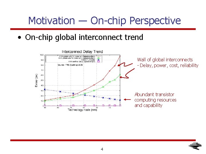
Motivation ― On-chip Perspective • On-chip global interconnect trend Wall of global interconnects - Delay, power, cost, reliability Abundant transistor computing resources and capability 4

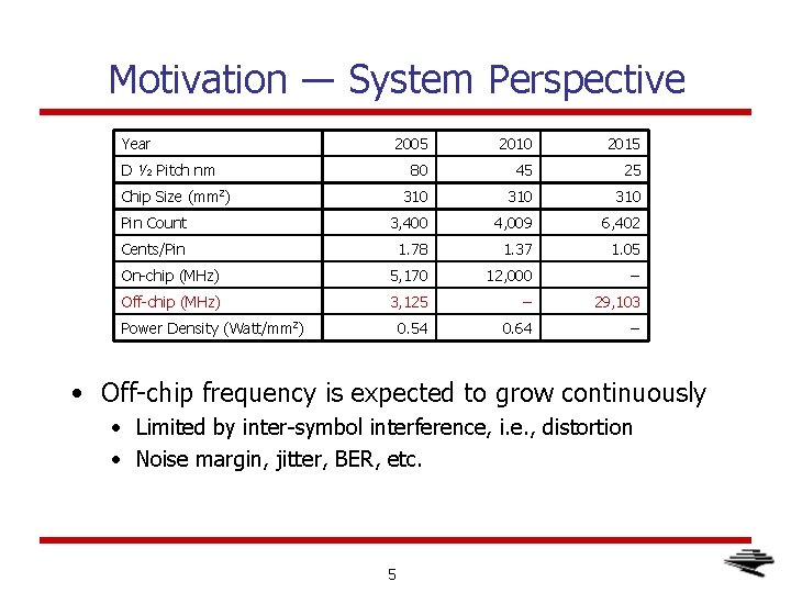
Motivation ― System Perspective Year 2005 2010 2015 80 45 25 310 310 Pin Count 3, 400 4, 009 6, 402 Cents/Pin 1. 78 1. 37 1. 05 On-chip (MHz) 5, 170 12, 000 − Off-chip (MHz) 3, 125 − 29, 103 0. 54 0. 64 − D ½ Pitch nm Chip Size (mm 2) Power Density (Watt/mm 2) • Off-chip frequency is expected to grow continuously • Limited by inter-symbol interference, i. e. , distortion • Noise margin, jitter, BER, etc. 5

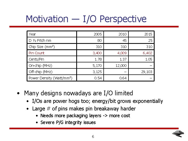
Motivation ― I/O Perspective Year 2005 2010 2015 80 45 25 310 310 Pin Count 3, 400 4, 009 6, 402 Cents/Pin 1. 78 1. 37 1. 05 On-chip (MHz) 5, 170 12, 000 − Off-chip (MHz) 3, 125 − 29, 103 0. 54 0. 64 − D ½ Pitch nm Chip Size (mm 2) Power Density (Watt/mm 2) • Many designs nowadays are I/O limited • I/Os are power hogs too; energy/bit grows exponentially • Large # of pins makes pin breakaway harder • Needs more packaging layers -> more cost • Severe P/G integrity issues 6

Outline • Motivation Previous Work • Surfliner • • Overview Theory Implementation Simulation Results • Applications • Conclusions 7

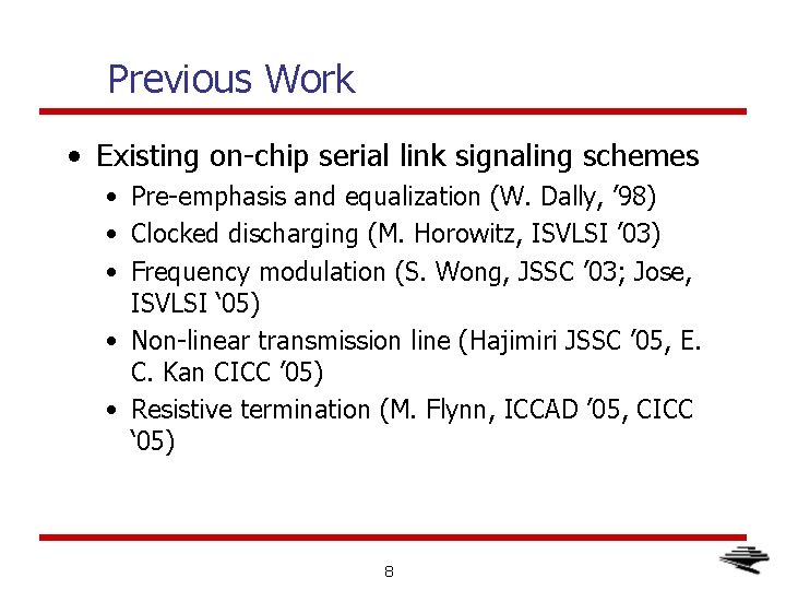
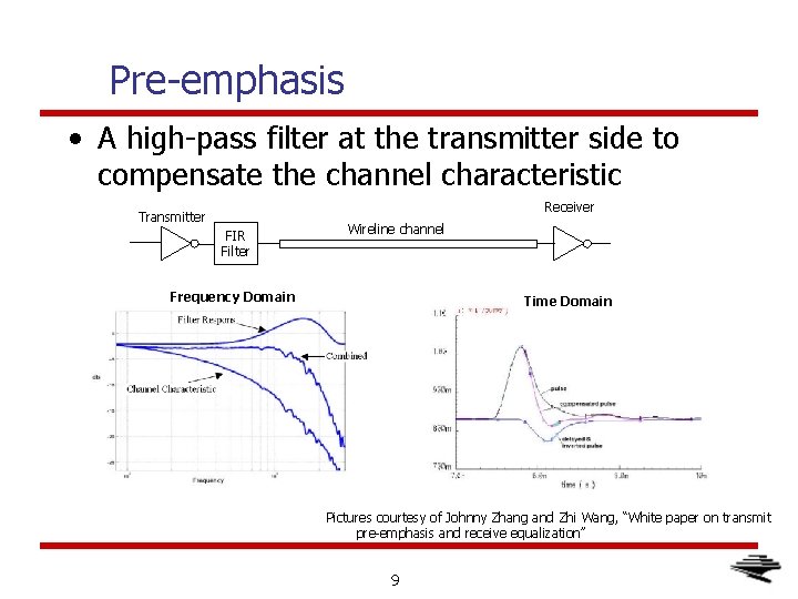
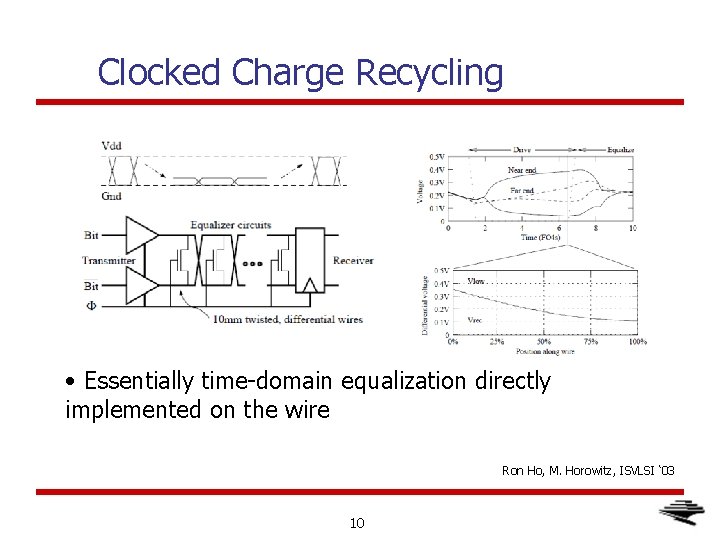
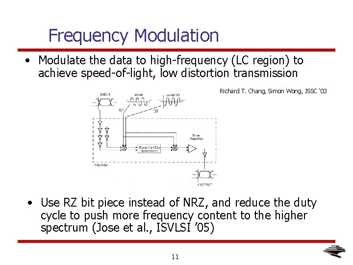
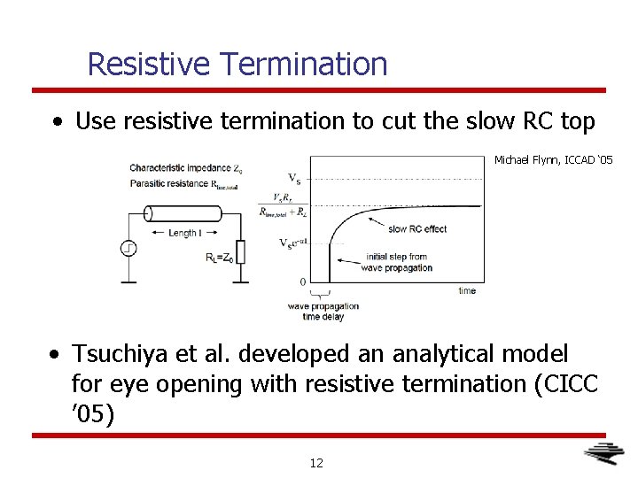
Previous Work • Existing on-chip serial link signaling schemes • Pre-emphasis and equalization (W. Dally, ’ 98) • Clocked discharging (M. Horowitz, ISVLSI ’ 03) • Frequency modulation (S. Wong, JSSC ’ 03; Jose, ISVLSI ‘ 05) • Non-linear transmission line (Hajimiri JSSC ’ 05, E. C. Kan CICC ’ 05) • Resistive termination (M. Flynn, ICCAD ’ 05, CICC ‘ 05) 8

Pre-emphasis • A high-pass filter at the transmitter side to compensate the channel characteristic Receiver Transmitter FIR Filter Wireline channel Frequency Domain Time Domain Pictures courtesy of Johnny Zhang and Zhi Wang, “White paper on transmit pre-emphasis and receive equalization” 9

Clocked Charge Recycling • Essentially time-domain equalization directly implemented on the wire Ron Ho, M. Horowitz, ISVLSI ‘ 03 10

Frequency Modulation • Modulate the data to high-frequency (LC region) to achieve speed-of-light, low distortion transmission Richard T. Chang, Simon Wong, JSSC ‘ 03 • Use RZ bit piece instead of NRZ, and reduce the duty cycle to push more frequency content to the higher spectrum (Jose et al. , ISVLSI ’ 05) 11

Resistive Termination • Use resistive termination to cut the slow RC top Michael Flynn, ICCAD ‘ 05 • Tsuchiya et al. developed an analytical model for eye opening with resistive termination (CICC ’ 05) 12

Outline • Motivation • Previous Work Surfliner • • Overview Theory Implementation Simulation Results • Applications • Conclusions 13

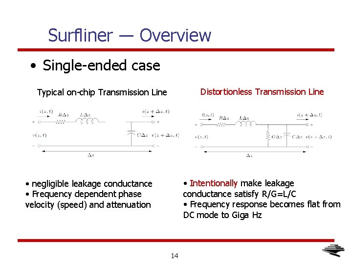
Surfliner ― Overview • Single-ended case Distortionless Transmission Line Typical on-chip Transmission Line • Intentionally make leakage conductance satisfy R/G=L/C • Frequency response becomes flat from DC mode to Giga Hz • negligible leakage conductance • Frequency dependent phase velocity (speed) and attenuation 14

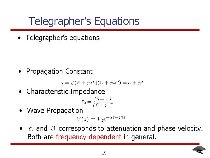
Telegrapher’s Equations • Telegrapher’s equations • Propagation Constant • Characteristic Impedance • Wave Propagation • and corresponds to attenuation and phase velocity. Both are frequency dependent in general. 15

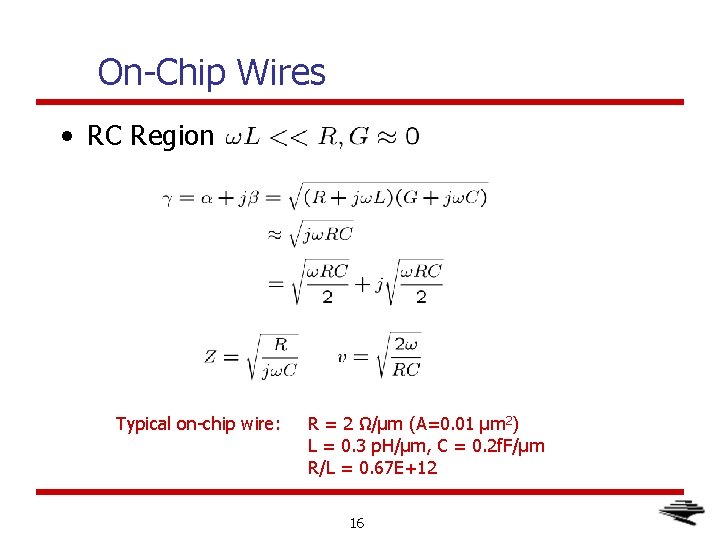
On-Chip Wires • RC Region Typical on-chip wire: R = 2 Ω/μm (A=0. 01 μm 2) L = 0. 3 p. H/μm, C = 0. 2 f. F/μm R/L = 0. 67 E+12 16

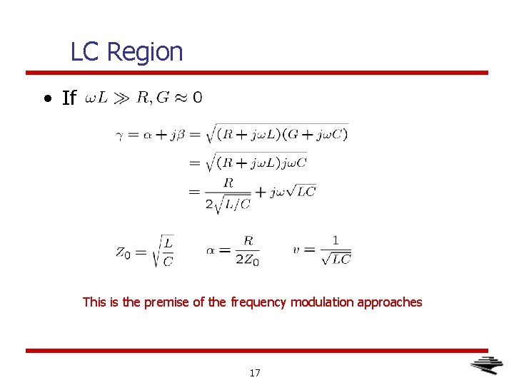
LC Region • If This is the premise of the frequency modulation approaches 17

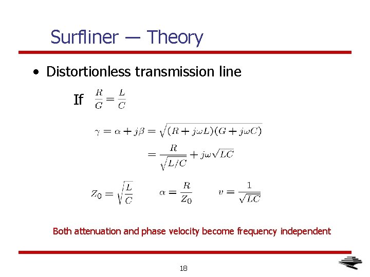
Surfliner ― Theory • Distortionless transmission line If Both attenuation and phase velocity become frequency independent 18

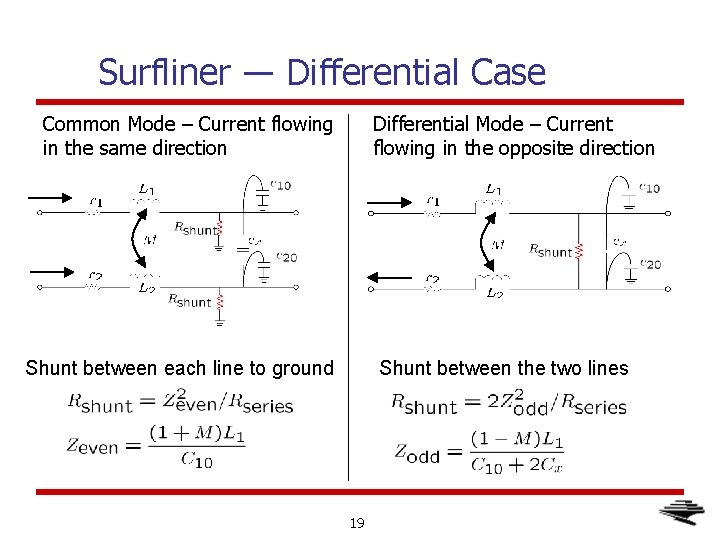
Surfliner ― Differential Case Common Mode – Current flowing in the same direction Differential Mode – Current flowing in the opposite direction Shunt between each line to ground Shunt between the two lines 19

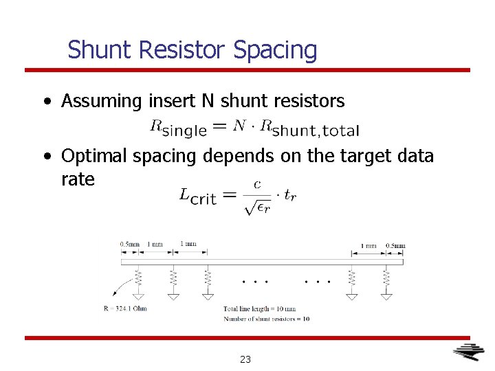
Surfliner ― Implementation • Evenly add shunt resistors between the signal line and the ground Ideal Surfliner In Practical Implication Homogeneous and distributive Discrete What’s the optimal spacing? Are the shunt resistors realizable? RLGC vary over frequency What’s the optimal frequency to do the matching? • Non-ideality RLGC are frequency independent 20

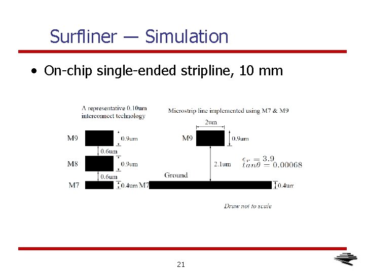
Surfliner ― Simulation • On-chip single-ended stripline, 10 mm 21

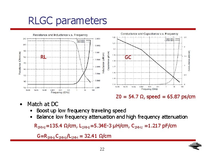
RLGC parameters RL GC Z 0 = 54. 7 Ω, speed = 65. 87 ps/cm • Match at DC • Boost up low frequency traveling speed • Balance low frequency attenuation and high frequency attenuation R 1 MHz=135. 4 Ω/cm, L 1 MHz=5. 34 E-3 μH/cm, C 1 MHz =1. 217 p. F/cm G=R 1 MHz. C 1 MHz/L 1 MH = 32. 41 Ω/cm 22

Shunt Resistor Spacing • Assuming insert N shunt resistors • Optimal spacing depends on the target data rate 23

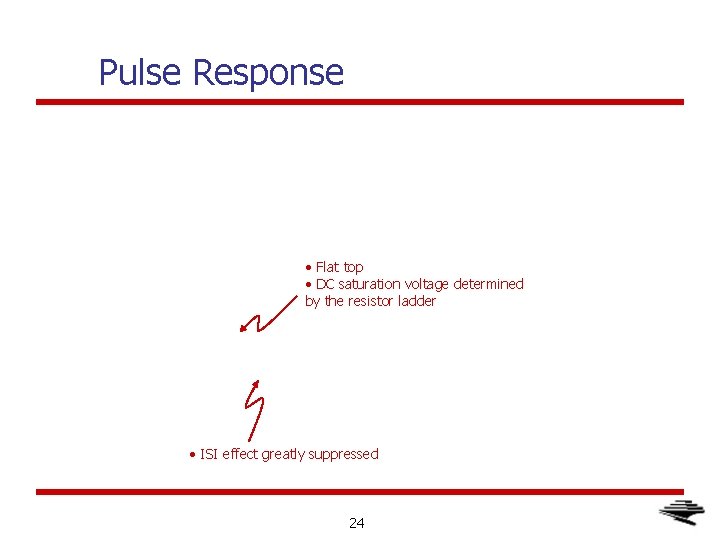
Pulse Response • Flat top • DC saturation voltage determined by the resistor ladder • ISI effect greatly suppressed 24

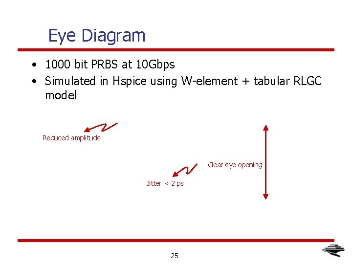
Eye Diagram • 1000 bit PRBS at 10 Gbps • Simulated in Hspice using W-element + tabular RLGC model Reduced amplitude Clear eye opening Jitter < 2 ps 25

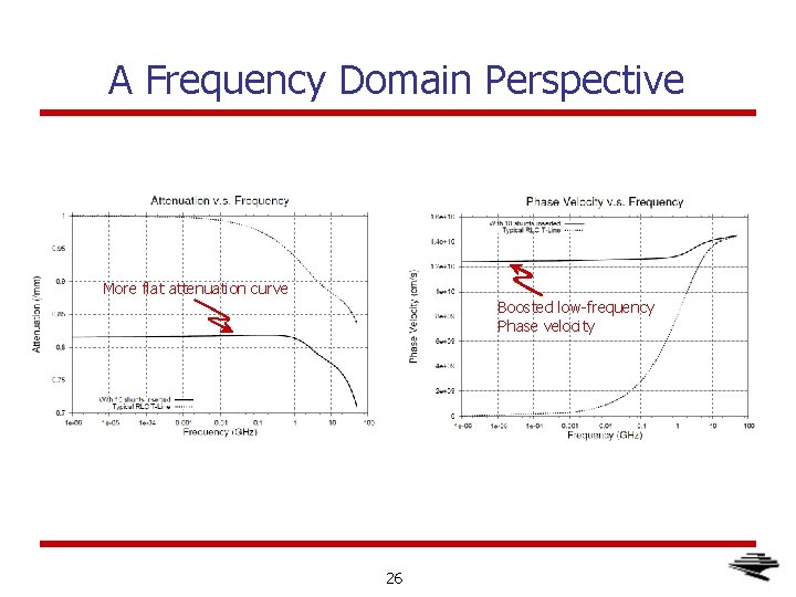
A Frequency Domain Perspective More flat attenuation curve Boosted low-frequency Phase velocity 26

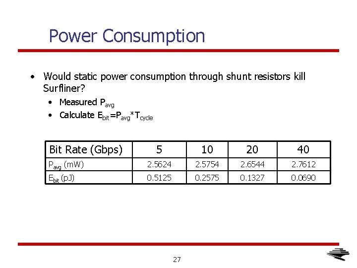
Power Consumption • Would static power consumption through shunt resistors kill Surfliner? • Measured Pavg • Calculate Ebit=Pavg*Tcycle Bit Rate (Gbps) 5 10 20 40 Pavg (m. W) 2. 5624 2. 5754 2. 6544 2. 7612 Ebit (p. J) 0. 5125 0. 2575 0. 1327 0. 0690 27

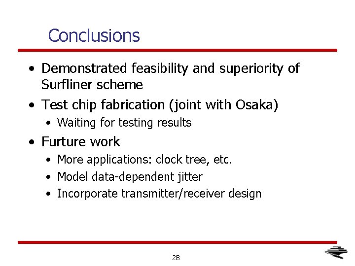
Conclusions • Demonstrated feasibility and superiority of Surfliner scheme • Test chip fabrication (joint with Osaka) • Waiting for testing results • Furture work • More applications: clock tree, etc. • Model data-dependent jitter • Incorporate transmitter/receiver design 28

The End Thank you! 29