Surface micromachining http www darpa milmtomems How a
- Slides: 27

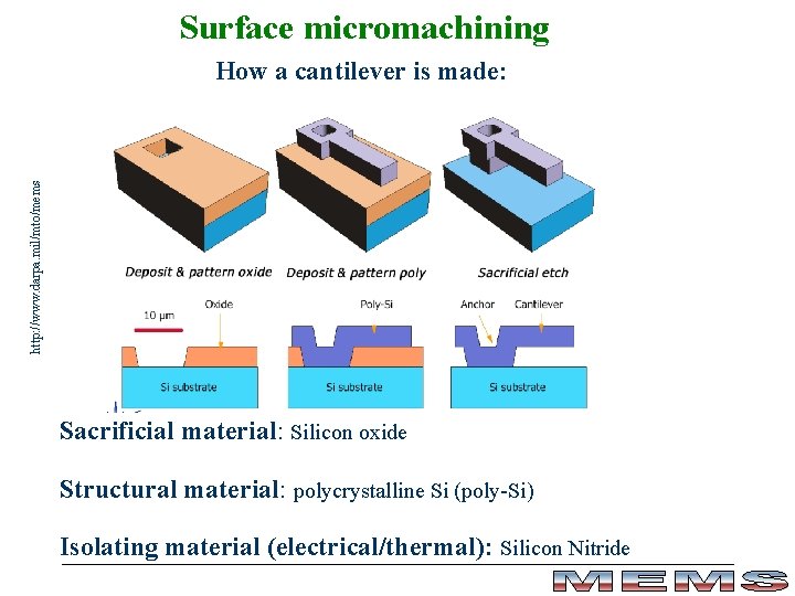
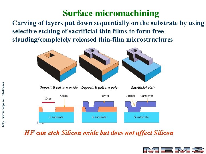
Surface micromachining http: //www. darpa. mil/mto/mems How a cantilever is made: Sacrificial material: Silicon oxide Structural material: polycrystalline Si (poly-Si) Isolating material (electrical/thermal): Silicon Nitride

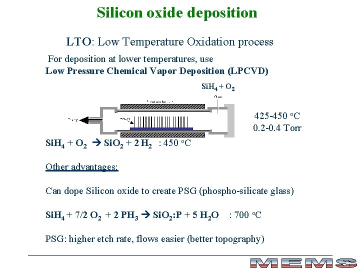
Silicon oxide deposition LTO: Low Temperature Oxidation process For deposition at lower temperatures, use Low Pressure Chemical Vapor Deposition (LPCVD) Si. H 4 + O 2 425 -450 o. C 0. 2 -0. 4 Torr Si. H 4 + O 2 Si. O 2 + 2 H 2 : 450 o. C Other advantages: Can dope Silicon oxide to create PSG (phospho-silicate glass) Si. H 4 + 7/2 O 2 + 2 PH 3 Si. O 2: P + 5 H 2 O : 700 o. C PSG: higher etch rate, flows easier (better topography)

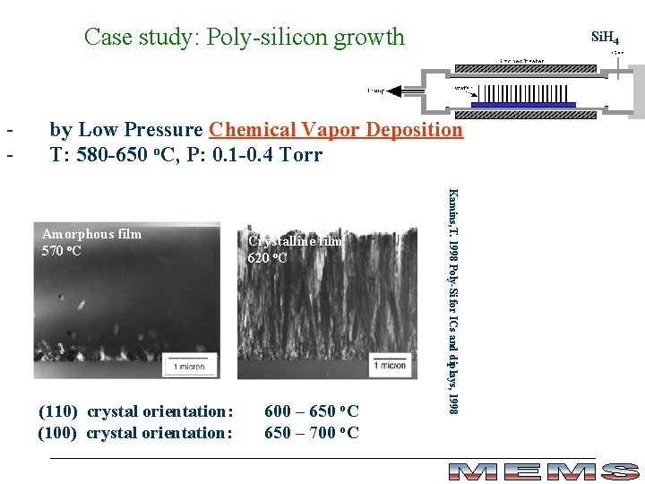
Case study: Poly-silicon growth - Si. H 4 by Low Pressure Chemical Vapor Deposition T: 580 -650 o. C, P: 0. 1 -0. 4 Torr Crystalline film 620 o. C Effect of temperature Amorphous Crystalline: Equi-axed grains: Columnar grains: (110) crystal orientation: (100) crystal orientation: 570 o. C 600 o. C 625 o. C 600 – 650 o. C 650 – 700 o. C Kamins, T. 1998 Poly-Si for ICs and diplays, 1998 Amorphous film 570 o. C

Poly-silicon growth Temperature has to be very accurately controlled as grains grow with temperature, increasing surface roughness, causing loss of pattern resolution and stresses in MEMS Mechanisms of grain growth: 1. Strain induced growth - Minimize strain energy due to mechanical deformation, doping … - Grain growth time 2. Grain boundary growth - To reduce surface energy (and grain boundary area) - Grain growth (time)1/2 3. Impurity drag - Can accelerate/prevent grain boundary movement - Grain growth (time)1/3

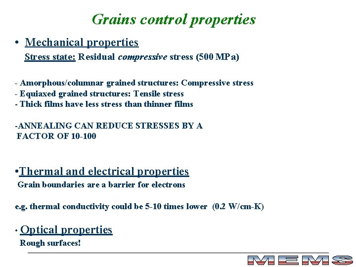
Grains control properties • Mechanical properties Stress state: Residual compressive stress (500 MPa) - Amorphous/columnar grained structures: Compressive stress - Equiaxed grained structures: Tensile stress - Thick films have less stress than thinner films -ANNEALING CAN REDUCE STRESSES BY A FACTOR OF 10 -100 • Thermal and electrical properties Grain boundaries are a barrier for electrons e. g. thermal conductivity could be 5 -10 times lower (0. 2 W/cm-K) • Optical properties Rough surfaces!

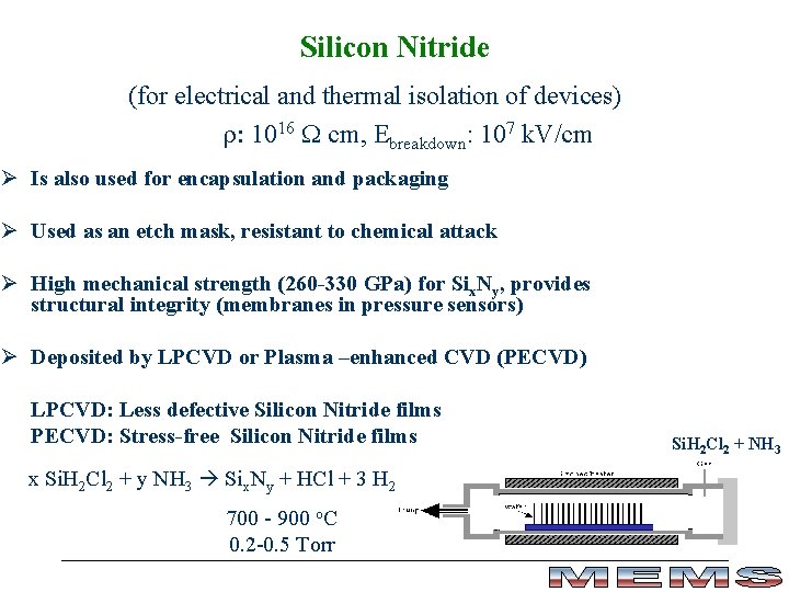
Silicon Nitride (for electrical and thermal isolation of devices) r: 1016 W cm, Ebreakdown: 107 k. V/cm Ø Is also used for encapsulation and packaging Ø Used as an etch mask, resistant to chemical attack Ø High mechanical strength (260 -330 GPa) for Six. Ny, provides structural integrity (membranes in pressure sensors) Ø Deposited by LPCVD or Plasma –enhanced CVD (PECVD) LPCVD: Less defective Silicon Nitride films PECVD: Stress-free Silicon Nitride films x Si. H 2 Cl 2 + y NH 3 Six. Ny + HCl + 3 H 2 700 - 900 o. C 0. 2 -0. 5 Torr Si. H 2 Cl 2 + NH 3

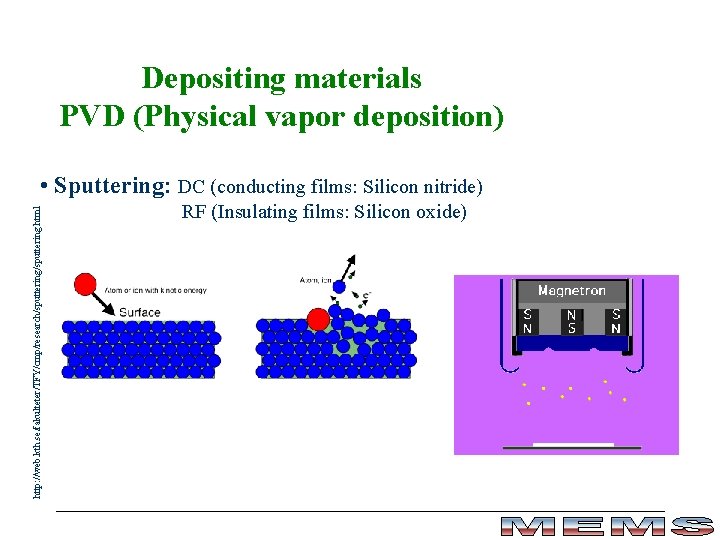
Depositing materials PVD (Physical vapor deposition) http: //web. kth. se/fakulteter/TFY/cmp/research/sputtering. html • Sputtering: DC (conducting films: Silicon nitride) RF (Insulating films: Silicon oxide)

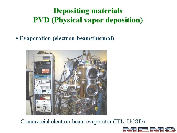
Depositing materials PVD (Physical vapor deposition) • Evaporation (electron-beam/thermal) Commercial electron-beam evaporator (ITL, UCSD)

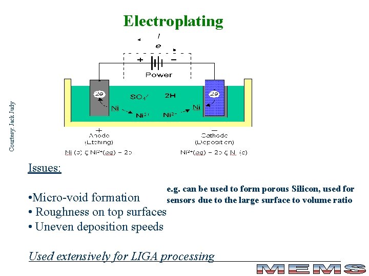
Courtesy: Jack Judy Electroplating Issues: e. g. can be used to form porous Silicon, used for sensors due to the large surface to volume ratio • Micro-void formation • Roughness on top surfaces • Uneven deposition speeds Used extensively for LIGA processing

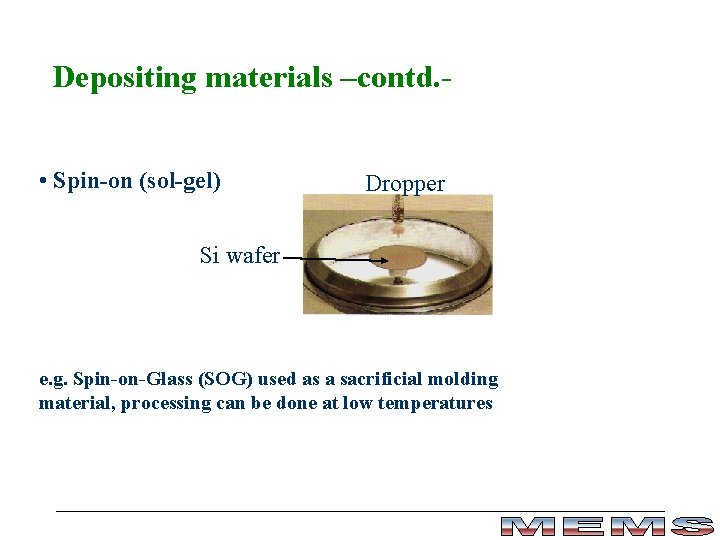
Depositing materials –contd. • Spin-on (sol-gel) Dropper Si wafer e. g. Spin-on-Glass (SOG) used as a sacrificial molding material, processing can be done at low temperatures

Surface micromachining - Technique and issues - Dry etching (DRIE) Other MEMS fabrication techniques - Micro-molding - LIGA Other materials in MEMS - Si. C, diamond, piezo-electrics, magnetic materials, shape memory alloys … MEMS foundry processes - How to make a micro-motor

Surface micromachining http: //www. darpa. mil/mto/mems Carving of layers put down sequentially on the substrate by using selective etching of sacrificial thin films to form freestanding/completely released thin-film microstructures HF can etch Silicon oxide but does not affect Silicon

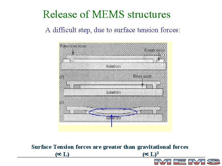
Release of MEMS structures A difficult step, due to surface tension forces: Surface Tension forces are greater than gravitational forces ( L)3

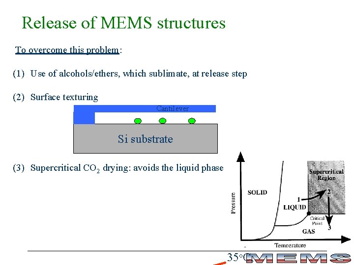
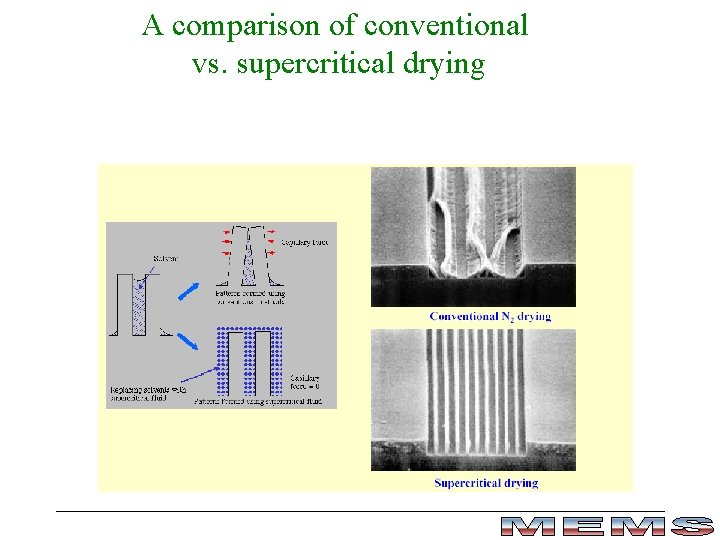
Release of MEMS structures To overcome this problem: (1) Use of alcohols/ethers, which sublimate, at release step (2) Surface texturing Cantilever Si substrate (3) Supercritical CO 2 drying: avoids the liquid phase 35 o. C,

A comparison of conventional vs. supercritical drying

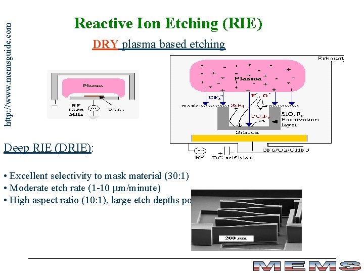
http: //www. memsguide. com Reactive Ion Etching (RIE) DRY plasma based etching Deep RIE (DRIE): • Excellent selectivity to mask material (30: 1) • Moderate etch rate (1 -10 mm/minute) • High aspect ratio (10: 1), large etch depths possible

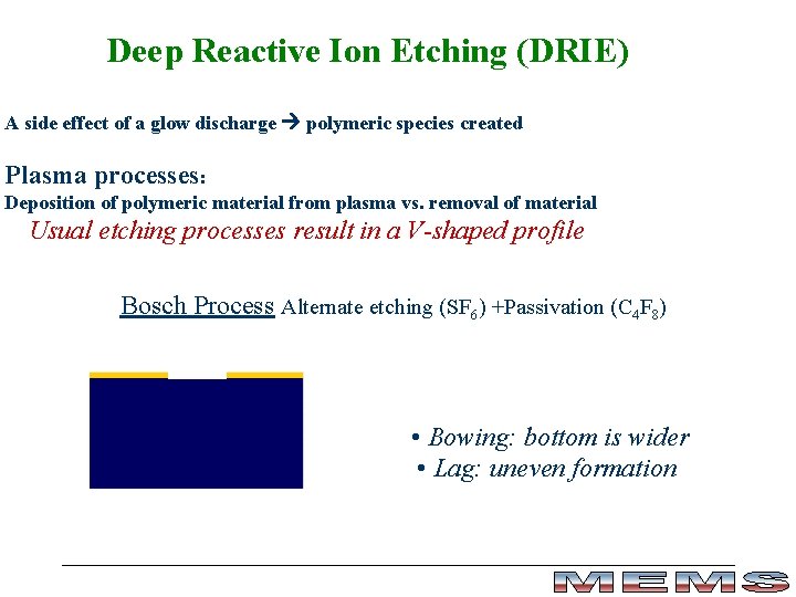
Deep Reactive Ion Etching (DRIE) A side effect of a glow discharge polymeric species created Plasma processes: Deposition of polymeric material from plasma vs. removal of material Usual etching processes result in a V-shaped profile Bosch Process Alternate etching (SF 6) +Passivation (C 4 F 8) • Bowing: bottom is wider • Lag: uneven formation

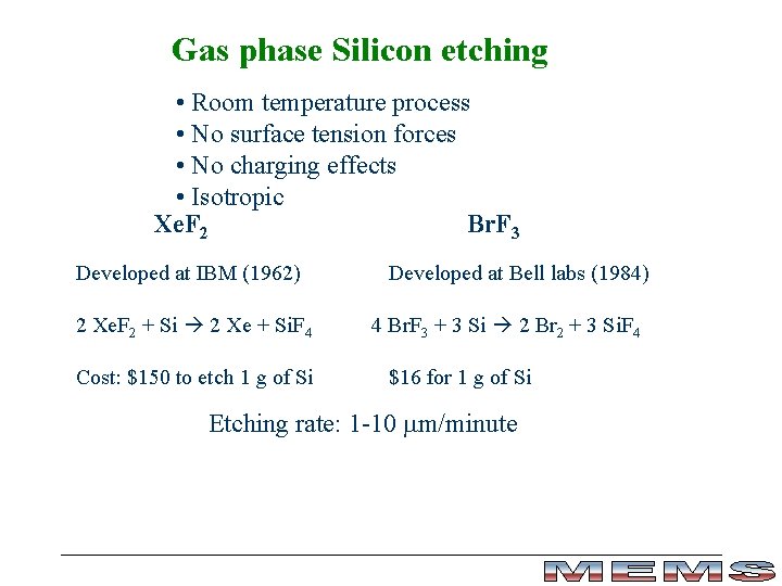
Gas phase Silicon etching • Room temperature process • No surface tension forces • No charging effects • Isotropic Xe. F 2 Br. F 3 Developed at IBM (1962) 2 Xe. F 2 + Si 2 Xe + Si. F 4 Cost: $150 to etch 1 g of Si Developed at Bell labs (1984) 4 Br. F 3 + 3 Si 2 Br 2 + 3 Si. F 4 $16 for 1 g of Si Etching rate: 1 -10 mm/minute

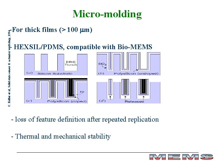
Micro-molding C. Keller et al, Solid state sensor & actuator workshop, 1994 -For thick films (> 100 mm) - HEXSIL/PDMS, compatible with Bio-MEMS - loss of feature definition after repeated replication - Thermal and mechanical stability

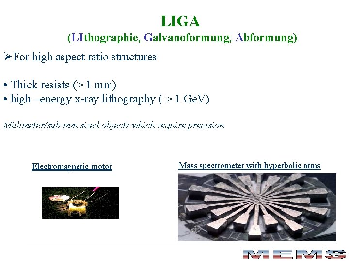
LIGA (LIthographie, Galvanoformung, Abformung) ØFor high aspect ratio structures • Thick resists (> 1 mm) • high –energy x-ray lithography ( > 1 Ge. V) Millimeter/sub-mm sized objects which require precision Electromagnetic motor Mass spectrometer with hyperbolic arms

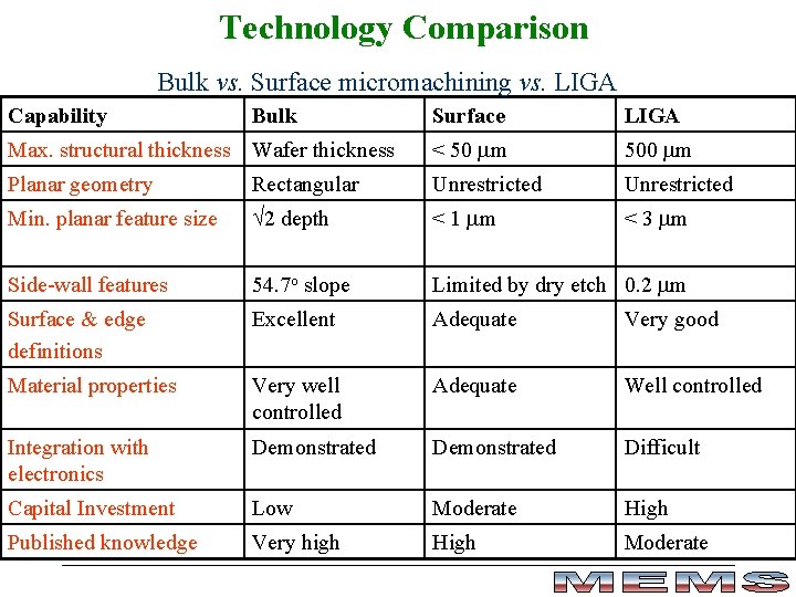
Technology Comparison Bulk vs. Surface micromachining vs. LIGA Capability Bulk Surface LIGA Max. structural thickness Wafer thickness < 50 mm 500 mm Planar geometry Rectangular Unrestricted Min. planar feature size 2 depth < 1 mm < 3 mm Side-wall features 54. 7 o slope Limited by dry etch 0. 2 mm Surface & edge definitions Excellent Adequate Very good Material properties Very well controlled Adequate Well controlled Integration with electronics Demonstrated Difficult Capital Investment Low Moderate High Published knowledge Very high High Moderate

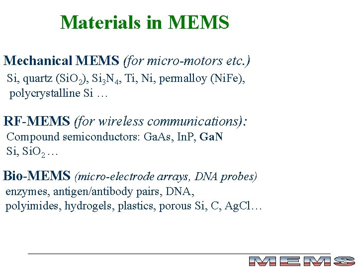
Materials in MEMS Mechanical MEMS (for micro-motors etc. ) Si, quartz (Si. O 2), Si 3 N 4, Ti, Ni, permalloy (Ni. Fe), polycrystalline Si … RF-MEMS (for wireless communications): Compound semiconductors: Ga. As, In. P, Ga. N Si, Si. O 2 … Bio-MEMS (micro-electrode arrays, DNA probes) enzymes, antigen/antibody pairs, DNA, polyimides, hydrogels, plastics, porous Si, C, Ag. Cl…

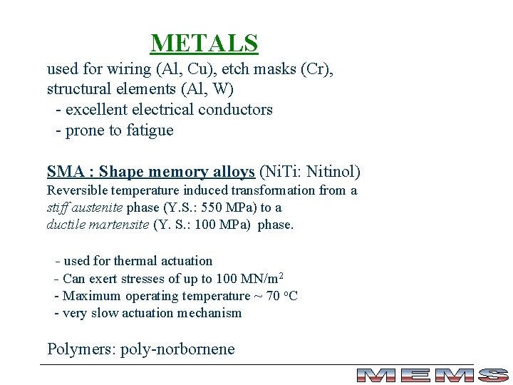
METALS used for wiring (Al, Cu), etch masks (Cr), structural elements (Al, W) - excellent electrical conductors - prone to fatigue SMA : Shape memory alloys (Ni. Ti: Nitinol) Reversible temperature induced transformation from a stiff austenite phase (Y. S. : 550 MPa) to a ductile martensite (Y. S. : 100 MPa) phase. - used for thermal actuation - Can exert stresses of up to 100 MN/m 2 - Maximum operating temperature ~ 70 o. C - very slow actuation mechanism Polymers: poly-norbornene

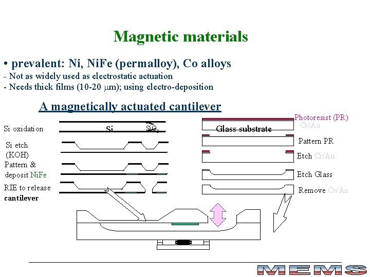
Magnetic materials • prevalent: Ni, Ni. Fe (permalloy), Co alloys - Not as widely used as electrostatic actuation - Needs thick films (10 -20 mm); using electro-deposition A magnetically actuated cantilever Si oxidation Si Si. O 2 Glass substrate Photoresist (PR) Cr/Au Pattern PR Si etch (KOH) Pattern & deposit Ni. Fe Etch Cr/Au RIE to release cantilever Remove Cr/Au Etch Glass

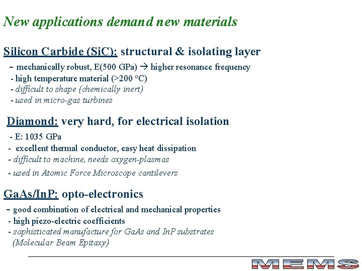
New applications demand new materials Silicon Carbide (Si. C): structural & isolating layer - mechanically robust, E(500 GPa) higher resonance frequency - high temperature material (>200 o. C) - difficult to shape (chemically inert) - used in micro-gas turbines Diamond: very hard, for electrical isolation - E: 1035 GPa - excellent thermal conductor, easy heat dissipation - difficult to machine, needs oxygen-plasmas - used in Atomic Force Microscope cantilevers Ga. As/In. P: opto-electronics - good combination of electrical and mechanical properties - high piezo-electric coefficients - sophisticated manufacture for Ga. As and In. P substrates (Molecular Beam Epitaxy)

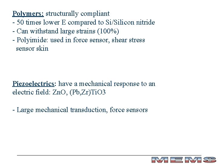
Polymers: structurally compliant - 50 times lower E compared to Si/Silicon nitride - Can withstand large strains (100%) - Polyimide: used in force sensor, shear stress sensor skin Piezoelectrics: have a mechanical response to an electric field: Zn. O, (Pb, Zr)Ti. O 3 - Large mechanical transduction, force sensors

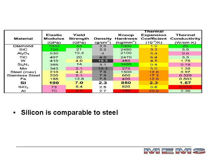
• Silicon is comparable to steel