School of Mathematical Sciences Nanocomputing memory devices and




- Slides: 22

School of Mathematical Sciences Nanocomputing memory devices and logic gates formed from carbon nanotubes and metallofullerenes Nanomechanics Group, School of Mathematical Sciences, The University of Adelaide, SA 5005, Australia Richard K. F. Lee and James M. Hill 5 th – 9 th February 2012 ICONN 2012, Perth, Western Australia Life Impact The University of Adelaide

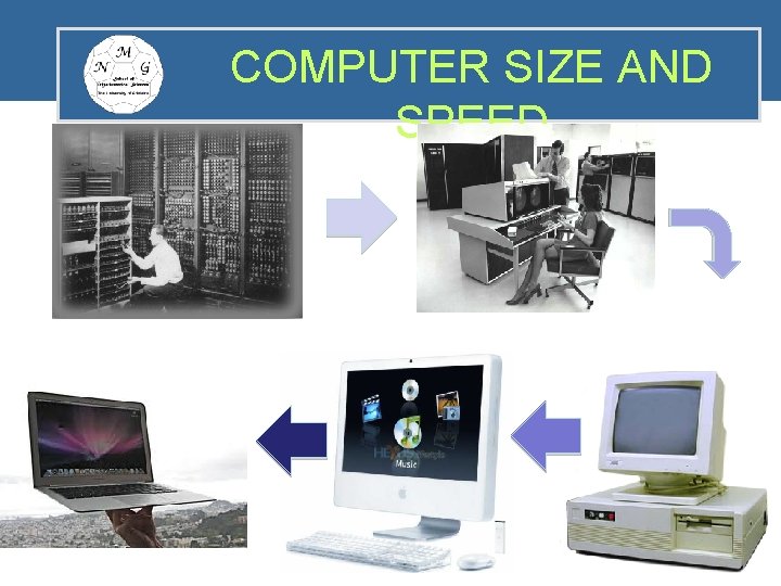
Overview • Trends in computer requirements: – Smaller in size, – Faster processing, – Increased data capacity. • Nano memory devices and logic gates: – Continuous approximation, – Lennard-Jones potential, – Memory devices and logic gates. • Conclusion 2

COMPUTER SIZE AND SPEED 3

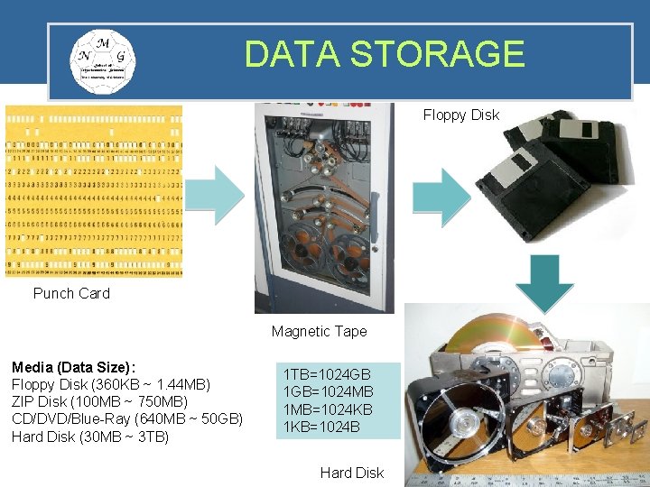
DATA STORAGE Floppy Disk Punch Card Magnetic Tape Media (Data Size): Floppy Disk (360 KB ~ 1. 44 MB) ZIP Disk (100 MB ~ 750 MB) CD/DVD/Blue-Ray (640 MB ~ 50 GB) Hard Disk (30 MB ~ 3 TB) 1 TB=1024 GB 1 GB=1024 MB 1 MB=1024 KB 1 KB=1024 B 4 Hard Disk

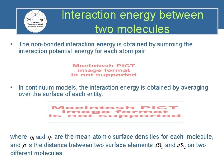
Interaction energy between two molecules • The non-bonded interaction energy is obtained by summing the interaction potential energy for each atom pair • In continuum models, the interaction energy is obtained by averaging over the surface of each entity. where h 1 and h 2 are the mean atomic surface densities for each molecule, and r is the distance between two surface elements d. S 1 and d. S 2 on two different molecules.

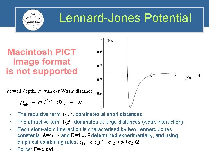
Lennard-Jones Potential : well depth, : van der Waals distance rmin = 21/6, Fmin = - • • The repulsive term 1/r 12, dominates at short distances, The attractive term 1/r 6, dominates at large distances (weak interaction), Each atom-atom interaction is characterised by two Lennard Jones constants, A=4 es 6 and B=4 es 12 determined experimentally, and using empirical combining rules, e 12=(e 1 e 2)1/2, s 12=(s 1+s 2)/2, Force: F=-d. F/dr.

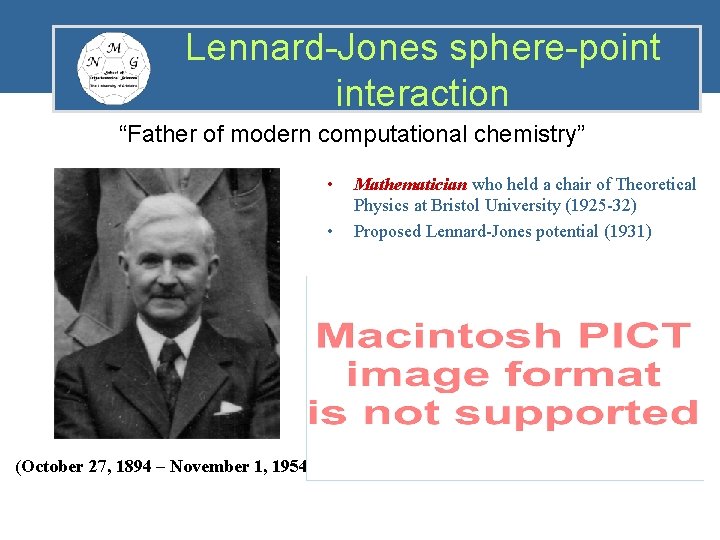
Lennard-Jones sphere-point interaction “Father of modern computational chemistry” • • (October 27, 1894 – November 1, 1954) Mathematician who held a chair of Theoretical Physics at Bristol University (1925 -32) Proposed Lennard-Jones potential (1931)

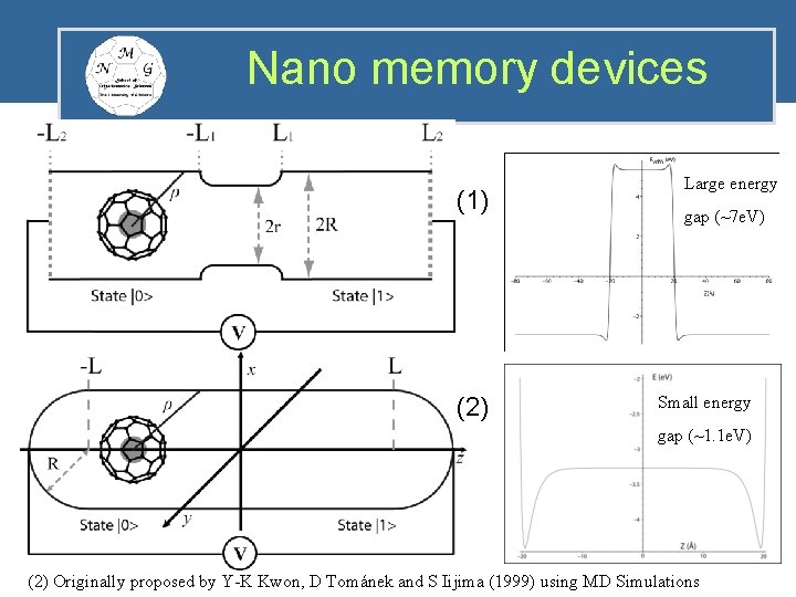
Nano memory devices (1) (2) Large energy gap (~7 e. V) Small energy gap (~1. 1 e. V) (2) Originally proposed by Y-K Kwon, D Tománek and S Iijima (1999) using MD Simulations

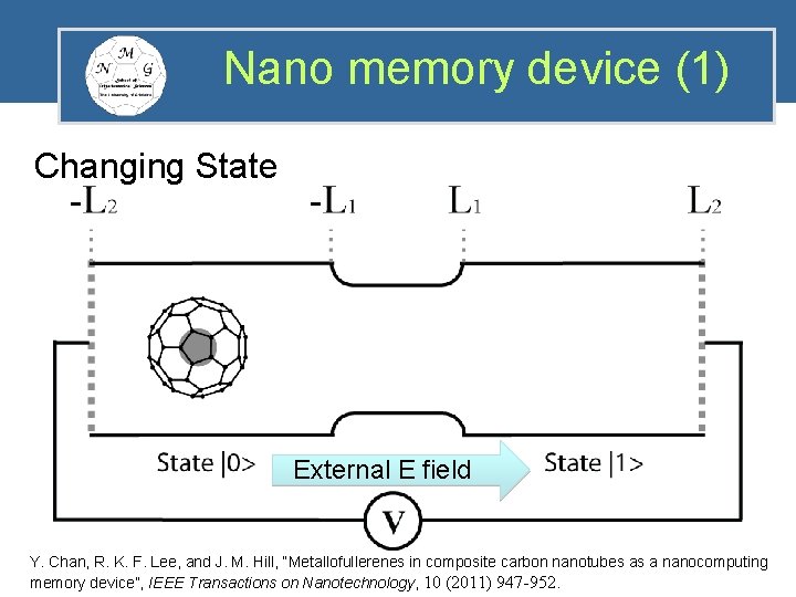
Nano memory device (1) Changing State External E field Y. Chan, R. K. F. Lee, and J. M. Hill, “Metallofullerenes in composite carbon nanotubes as a nanocomputing memory device”, IEEE Transactions on Nanotechnology, 10 (2011) 947 -952.

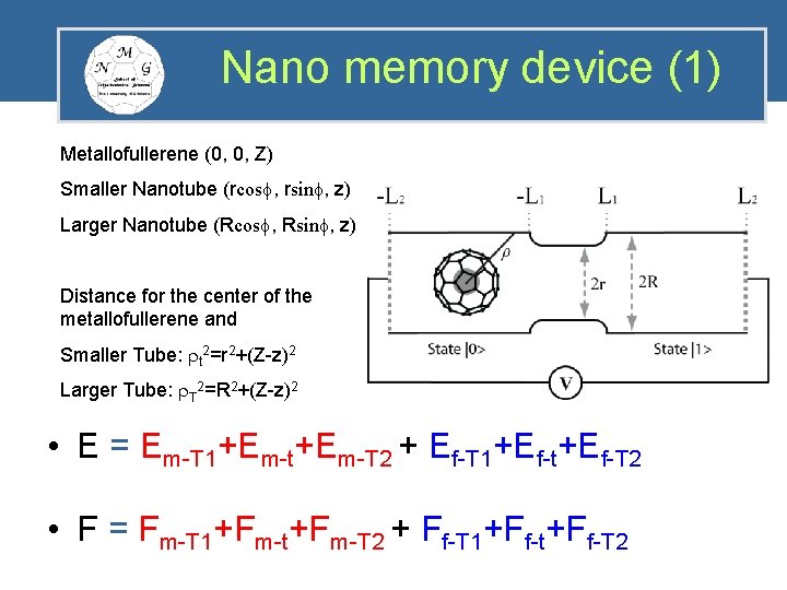
Nano memory device (1) Metallofullerene (0, 0, Z) Smaller Nanotube (rcosf, rsinf, z) Larger Nanotube (Rcosf, Rsinf, z) Distance for the center of the metallofullerene and Smaller Tube: rt 2=r 2+(Z-z)2 Larger Tube: r. T 2=R 2+(Z-z)2 • E = Em-T 1+Em-t+Em-T 2 + Ef-T 1+Ef-t+Ef-T 2 • F = Fm-T 1+Fm-t+Fm-T 2 + Ff-T 1+Ff-t+Ff-T 2

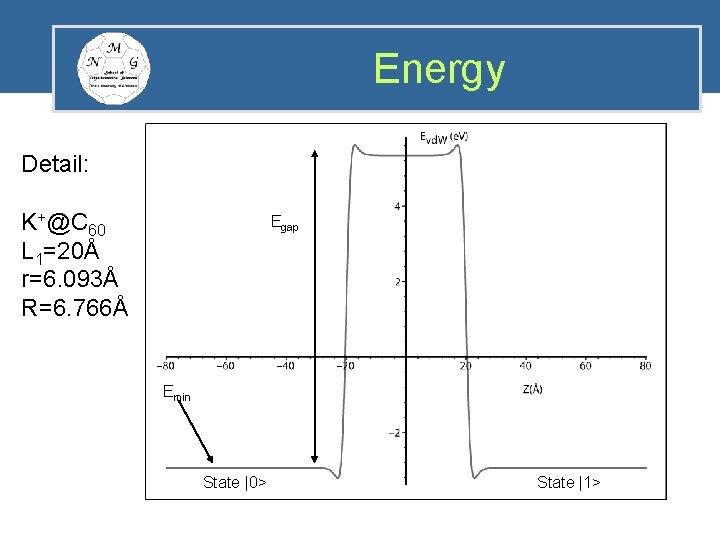
Energy Detail: K+@C 60 L 1=20Å r=6. 093Å R=6. 766Å Egap Emin State |0> State |1>

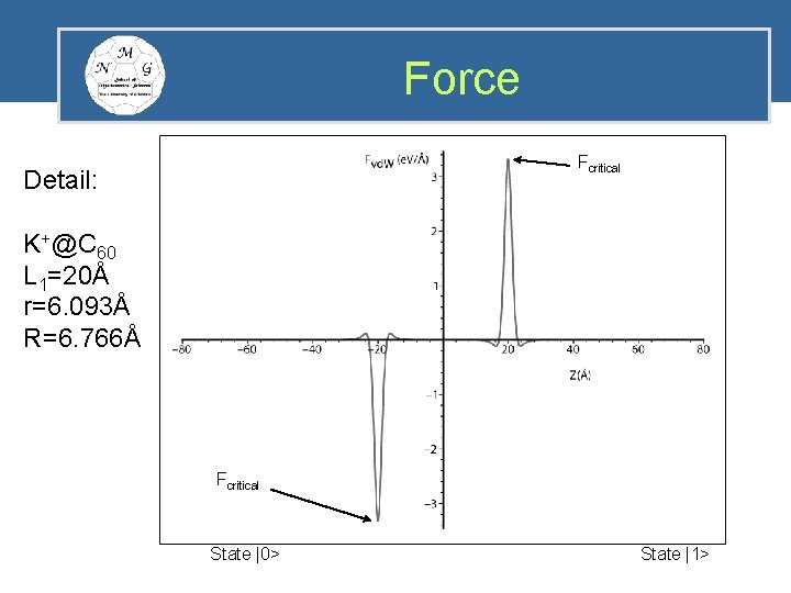
Force Fcritical Detail: K+@C 60 L 1=20Å r=6. 093Å R=6. 766Å Fcritical State |0> State |1>

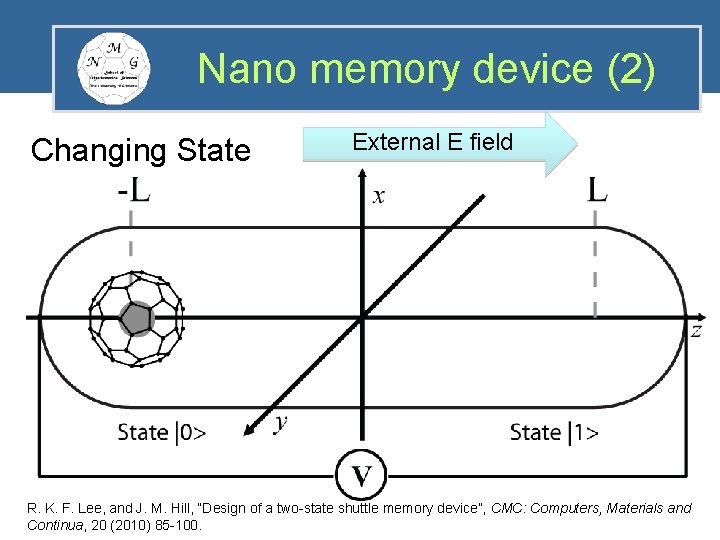
Nano memory device (2) Changing State External E field R. K. F. Lee, and J. M. Hill, “Design of a two-state shuttle memory device”, CMC: Computers, Materials and Continua, 20 (2010) 85 -100.

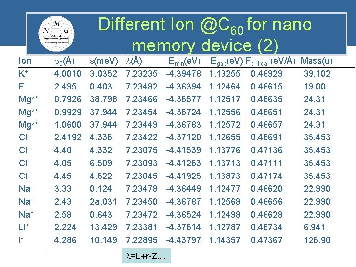
Ion K+ FMg 2+ Cl. Cl. Na+ Na+ Li+ I- r 0(Å) 4. 0010 2. 495 0. 7926 0. 9929 1. 0600 2. 4192 4. 40 4. 05 4. 45 3. 33 2. 43 2. 58 2. 224 4. 286 Different Ion @C 60 for nano memory device (2) e(me. V) 3. 0352 0. 403 38. 798 37. 944 4. 336 4. 332 6. 509 4. 622 0. 124 2 a. 031 0. 643 13. 429 10. 149 l(Å) 7. 23235 7. 23482 7. 23466 7. 23454 7. 23449 7. 23422 7. 23075 7. 23093 7. 23045 7. 23478 7. 23450 7. 23472 7. 23381 7. 22895 Emin(e. V) -4. 39478 -4. 36394 -4. 36577 -4. 36724 -4. 36783 -4. 37120 -4. 41539 -4. 41263 -4. 41925 -4. 36449 -4. 36787 -4. 36524 -4. 37614 -4. 43797 l=L+r-Zmin Egap(e. V) Fcritical (e. V/Å) 1. 13255 0. 46929 1. 12464 0. 46615 1. 12517 0. 46635 1. 12556 0. 46651 1. 12572 0. 46657 1. 12655 0. 46691 1. 13776 0. 47136 1. 13713 0. 47111 1. 13873 0. 47174 1. 12477 0. 46620 1. 12568 0. 46656 1. 12498 0. 46628 1. 12787 0. 46734 1. 14357 0. 47367 Mass(u) 39. 102 19. 00 24. 31 35. 453 22. 990 6. 941 126. 90

Transfer time for nano memory device (2) Example: K+@C 60 2 L=27Å, Fext=0. 5 e. V/Å tf=2. 4933 ps (1 ps=10 -12 s) State Switching Rate ~ 401 Gbit/s

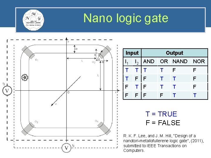
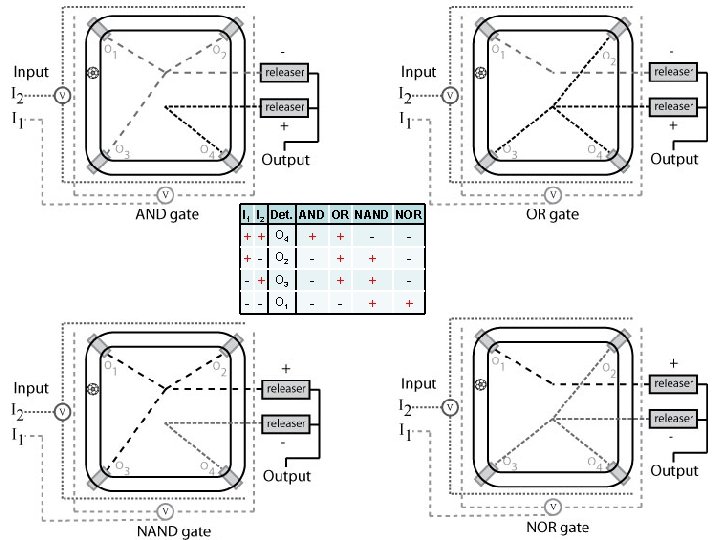
Nano logic gate Input Output I 1 I 2 AND OR NAND NOR T T F F T T F F F T T T = TRUE F = FALSE R. K. F. Lee, and J. M. Hill, “Design of a nanotori-metallofullerene logic gate”, (2011), submitted to IEEE Transactions on Computers.

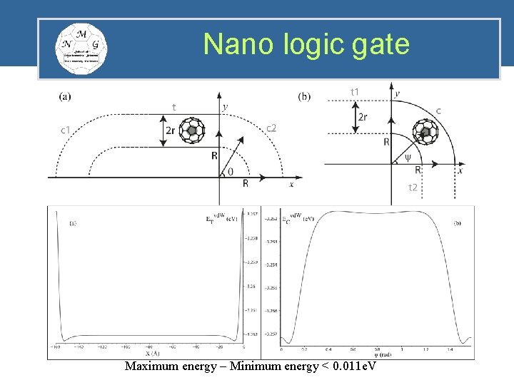
Nano logic gate Maximum energy – Minimum energy < 0. 011 e. V


Conclusion • Memory devices and logic gates: – Nano size, – Electrical field control. • For a fast state switching rate / time: – Light Ion, – Large external force, – Short nanotube length, – Around 400 Gbit/s.

Acknowledgement • All colleagues in the Nanomechanics Group • Australian Research Council http: //www. maths. adelaide. edu. au/nanomechanics/ 20

Thank you! http: //www. maths. adelaide. edu. au/nanomechanics/

References • G. E. Moore, Technical Digest International Electron Devices Meeting, 21 (1975) 11 -13. • B. J. Cox, N. Thamwattana and J. M. Hill, Proceedings of The Royal Society A, 463 (2007) 461 -476. • B. J. Cox, N. Thamwattana and J. M. Hill, Proceedings of The Royal Society A, 463 (2007) 477 -494. • Y. Chan, R. K. F. Lee and J. M. Hill, IEEE Transactions on Nanotechnology, 10 (2011) 947 -952. • R. K. F. Lee and J. M. Hill, CMC: Computers, Materials and Continua, 20 (2010) 85 -100. • R. K. F. Lee and J. M. Hill, “Design of a nanotori-metallofullerene logic gate”, (2011), submitted to IEEE Transactions on Computers.