Planar semiconductor Compton imaging using pulse shape analysis









- Slides: 24

Planar semiconductor Compton imaging using pulse shape analysis Anthony Sweeney Position Sensitive Detectors 9 Aberystwyth 2011

Outline • Motivation • Compton camera principles • Pulse shape analysis • Initial result • Silicon Detector • Future work

Motivation • Homeland security • Nuclear decommissioning • Existing systems are limited

Compton camera principles

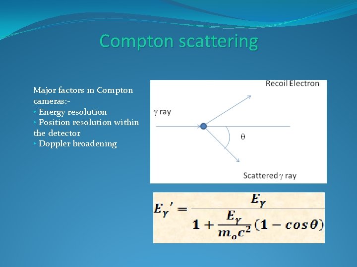
Compton scattering Major factors in Compton cameras: • Energy resolution • Position resolution within the detector • Doppler broadening

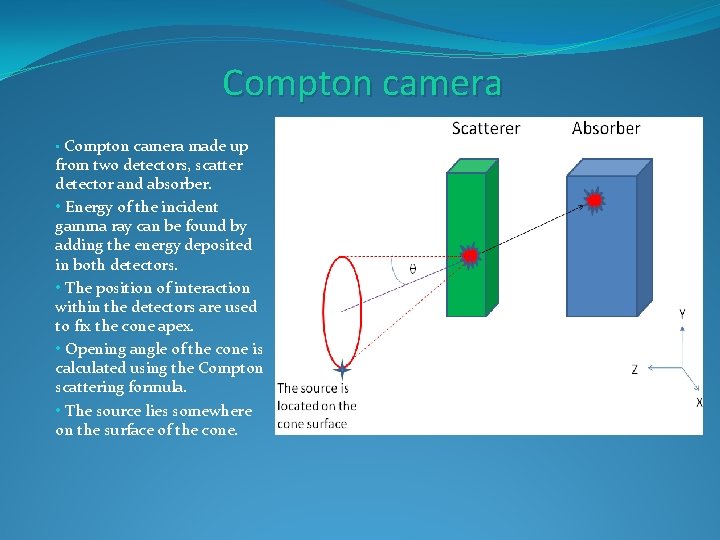
Compton camera • Compton camera made up from two detectors, scatter detector and absorber. • Energy of the incident gamma ray can be found by adding the energy deposited in both detectors. • The position of interaction within the detectors are used to fix the cone apex. • Opening angle of the cone is calculated using the Compton scattering formula. • The source lies somewhere on the surface of the cone.

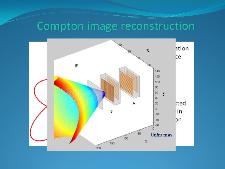
Compton image reconstruction x y z Units mm

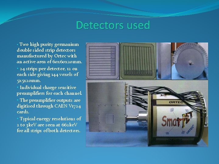
Detectors used • Two high purity germanium double sided strip detectors manufactured by Ortec with an active area of 60 x 20 mm. • 24 strips per detector, 12 on each side giving 144 voxels of 5 x 5 x 20 mm. • Individual charge sensitive preamplifiers for each channel. • The preamplifier outputs are digitised through CAEN V 1724 cards. • Typical energy resolutions of 2 to 3 ke. V are seen at 662 ke. V for all strips of both detectors.

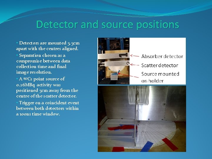
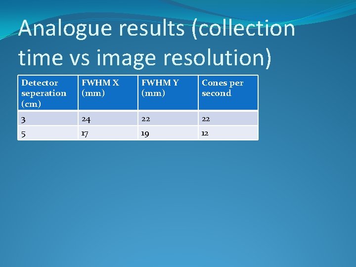
Detector and source positions • Detectors are mounted 5. 5 cm apart with the centres aligned. • Separation chosen as a compromise between data collection time and final image resolution. • A 137 Cs point source of 0. 26 MBq activity was positioned 5 cm away from the centre of the scatter detector. • Trigger on a coincident event between both detectors within a 100 ns time window.

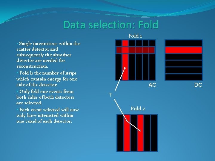
Data selection: Fold 1 • Single interactions within the scatter detector and subsequently the absorber detector are needed for reconstruction. • Fold is the number of strips which contain energy for one side of the detector. • Only fold one events from both sides of both detectors are selected. • Each event selected will now only have interacted within one voxel of each detector. AC g Fold 2 DC

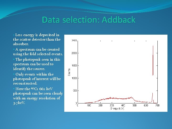
Data selection: Addback • Less energy is deposited in the scatter detector than the absorber. • A spectrum can be created using the fold selected events. • The photopeak seen in this spectrum can be used to identify the source. • Only events within the photopeak of interest will be reconstructed. • Here the 137 Cs 662 ke. V photopeak can be seen clearly with an energy resolution of 3. 7 ke. V.

Pulse shape analysis (PSA)

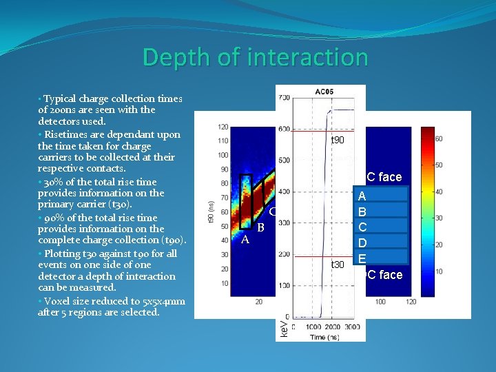
Depth of interaction • Typical charge collection times t 90 AC face E D C A B t 30 ke. V of 200 ns are seen with the detectors used. • Risetimes are dependant upon the time taken for charge carriers to be collected at their respective contacts. • 30% of the total rise time provides information on the primary carrier (t 30). • 90% of the total rise time provides information on the complete charge collection (t 90). • Plotting t 30 against t 90 for all events on one side of one detector a depth of interaction can be measured. • Voxel size reduced to 5 x 5 x 4 mm after 5 regions are selected. A B C D E DC face

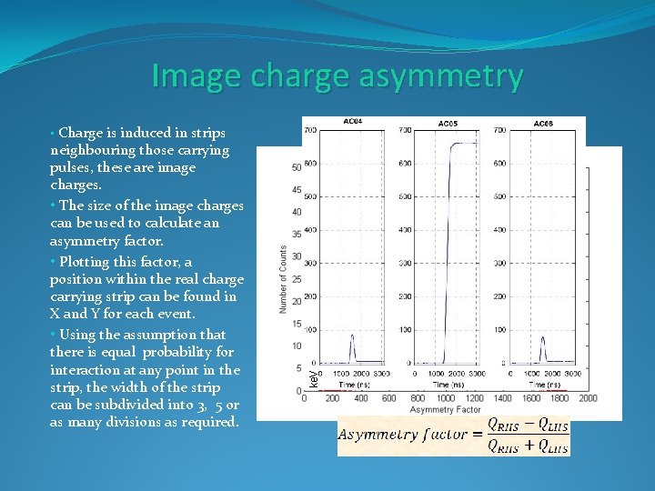
Image charge asymmetry neighbouring those carrying pulses, these are image charges. • The size of the image charges can be used to calculate an asymmetry factor. • Plotting this factor, a position within the real charge carrying strip can be found in X and Y for each event. • Using the assumption that there is equal probability for interaction at any point in the strip, the width of the strip can be subdivided into 3, 5 or as many divisions as required. ke. V • Charge is induced in strips

Initial results

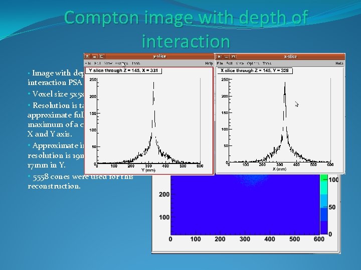
Compton image with depth of interaction • Image with depth of interaction PSA applied. • Voxel size 5 x 5 x 5 mm. • Resolution is taken as an approximate full width half maximum of a cut through the X and Y axis. • Approximate image resolution is 19 mm in X and 17 mm in Y. • 5558 cones were used for this reconstruction.

Silicon detector

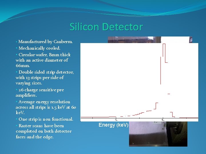
Silicon Detector • Manufactured by Canberra. • Mechanically cooled. • Circular wafer, 8 mm thick with an active diameter of 66 mm. • Double sided strip detector, with 13 strips per side of varying sizes. • 26 charge sensitive pre amplifiers. • Average energy resolution across all strips is 1. 5 ke. V at 60 ke. V. • One strip is non functional. • Raster scans have been completed on both detector faces and the edge. Energy (ke. V)

Future work

Future work Asymmetry pulse shape analysis will be applied to the data. New firmware is being tested for the CAEN V 1724 s. Compton data will be collected with the silicon detector acting as the scatter detector. A 5 mm thick HPGe detector will be scanned and tested to provide an additional scatter detector opening the possibility of a three detector Compton camera system. Tests onsite at Aldermaston.


Contributors Andrew J. Bostona, Helen C. Bostona, John R. Cresswella, Jamie Dormanda, Mark Ellisb, Laura J. Harknessa, Martin Jonesa, Daniel S. Judsona, Paul J. Nolana, David C. Oxleya, David P. Scraggsa, Mike J. Sleea, Amandeep Thandib a. Department of Physics, University of Liverpool, L 69 7 ZE, United Kingdom b. Atomic Weapons Establishment (AWE), Aldermaston, Reading, RG 7 4 PR, United Kingdom

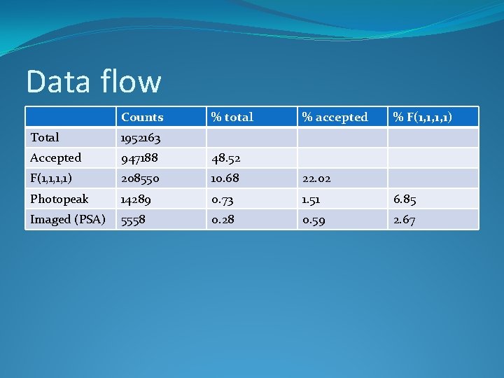
Data flow Counts % total % accepted % F(1, 1, 1, 1) Total 1952163 Accepted 947188 48. 52 F(1, 1, 1, 1) 208550 10. 68 22. 02 Photopeak 14289 0. 73 1. 51 6. 85 Imaged (PSA) 5558 0. 28 0. 59 2. 67

Analogue results (collection time vs image resolution) Detector seperation (cm) FWHM X (mm) FWHM Y (mm) Cones per second 3 24 22 22 5 17 19 12