PGT 202 Analog Electronic I Lecture 1 Semiconductor

- Slides: 22

PGT 202 Analog Electronic I Lecture 1 Semiconductor Material

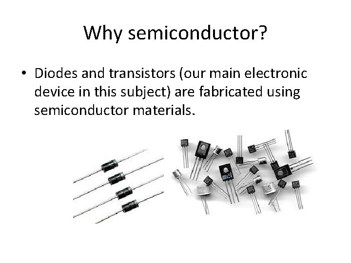
Why semiconductor? • Diodes and transistors (our main electronic device in this subject) are fabricated using semiconductor materials.

Intrinsic Semiconductors • Ideally 100% pure material – Elemental semiconductors • Silicon (Si) – Most common semiconductor used today • Germanium (Ge) – First semiconductor used in p-n diodes – Compound semiconductors • Gallium Arsenide (Ga. As)

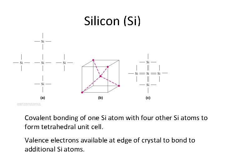
Silicon (Si) Covalent bonding of one Si atom with four other Si atoms to form tetrahedral unit cell. Valence electrons available at edge of crystal to bond to additional Si atoms.

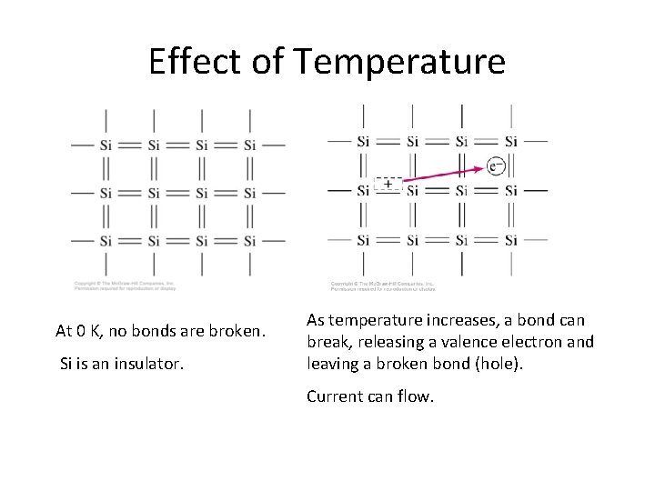
Effect of Temperature At 0 K, no bonds are broken. Si is an insulator. As temperature increases, a bond can break, releasing a valence electron and leaving a broken bond (hole). Current can flow.

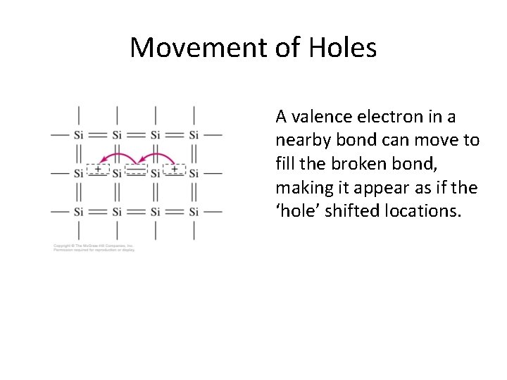
Movement of Holes A valence electron in a nearby bond can move to fill the broken bond, making it appear as if the ‘hole’ shifted locations.

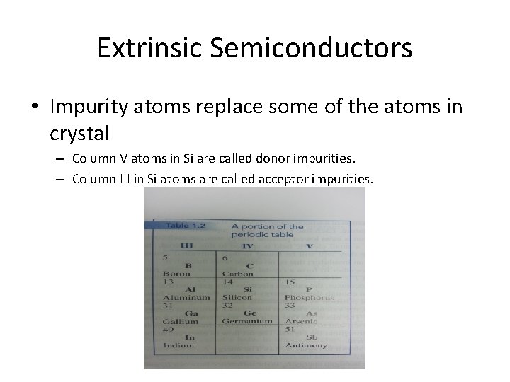
Extrinsic Semiconductors • Impurity atoms replace some of the atoms in crystal – Column V atoms in Si are called donor impurities. – Column III in Si atoms are called acceptor impurities.

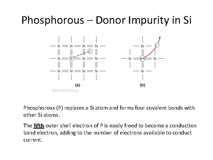
Phosphorous – Donor Impurity in Si Phosphorous (P) replaces a Si atom and forms four covalent bonds with other Si atoms. The fifth outer shell electron of P is easily freed to become a conduction band electron, adding to the number of electrons available to conduct current.

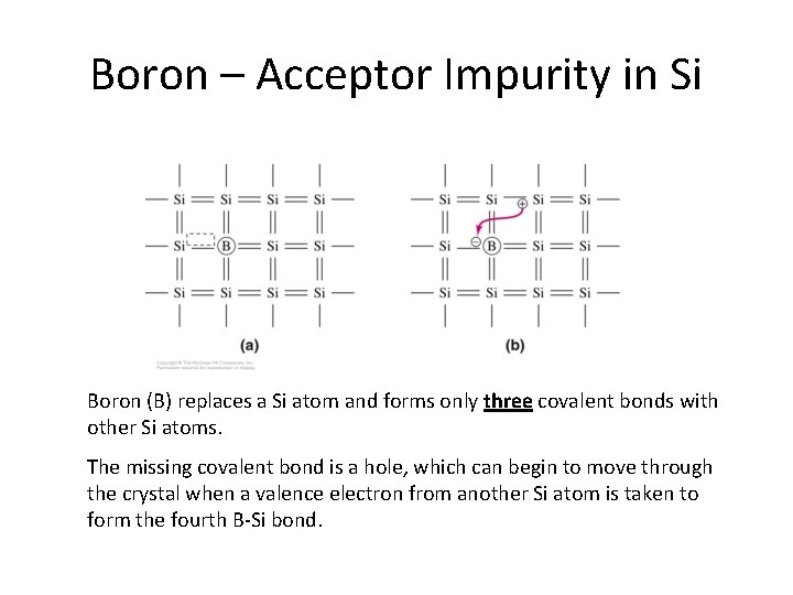
Boron – Acceptor Impurity in Si Boron (B) replaces a Si atom and forms only three covalent bonds with other Si atoms. The missing covalent bond is a hole, which can begin to move through the crystal when a valence electron from another Si atom is taken to form the fourth B-Si bond.

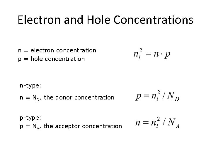
Electron and Hole Concentrations n = electron concentration p = hole concentration n-type: n = ND, the donor concentration p-type: p = NA, the acceptor concentration

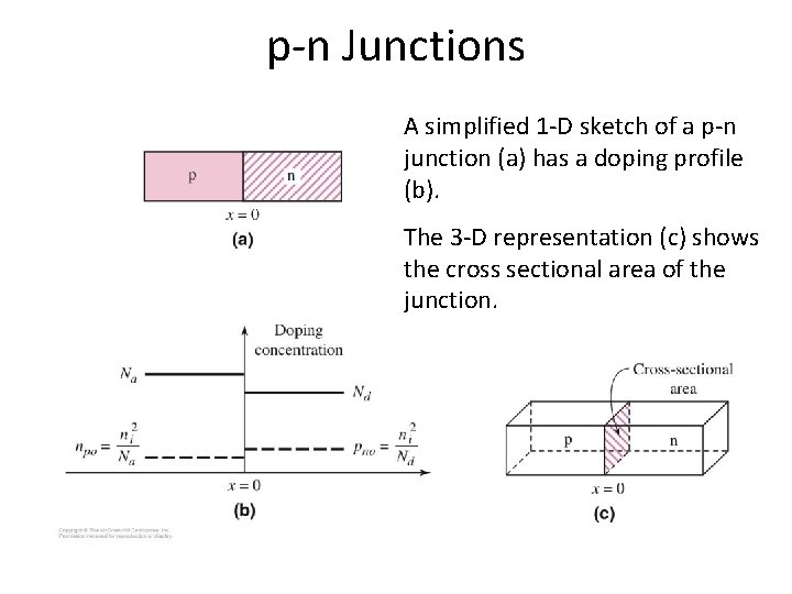
p-n Junctions A simplified 1 -D sketch of a p-n junction (a) has a doping profile (b). The 3 -D representation (c) shows the cross sectional area of the junction.

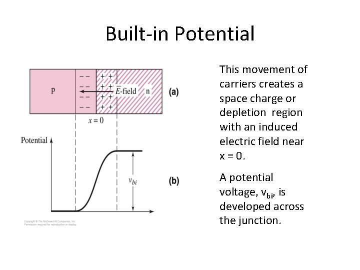
Built-in Potential This movement of carriers creates a space charge or depletion region with an induced electric field near x = 0. A potential voltage, vbi, is developed across the junction.

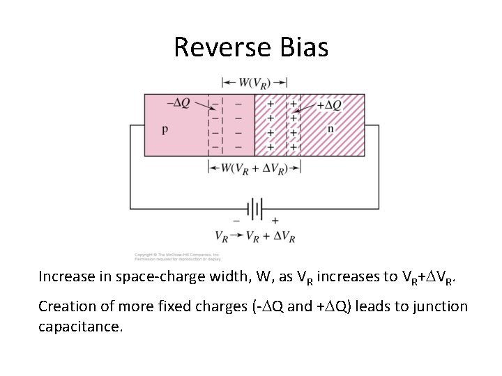
Reverse Bias Increase in space-charge width, W, as VR increases to VR+DVR. Creation of more fixed charges (-DQ and +DQ) leads to junction capacitance.

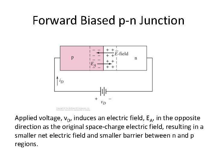
Forward Biased p-n Junction Applied voltage, v. D, induces an electric field, EA, in the opposite direction as the original space-charge electric field, resulting in a smaller net electric field and smaller barrier between n and p regions.

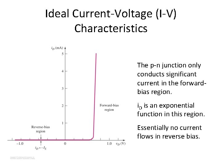
Ideal Current-Voltage (I-V) Characteristics The p-n junction only conducts significant current in the forwardbias region. i. D is an exponential function in this region. Essentially no current flows in reverse bias.

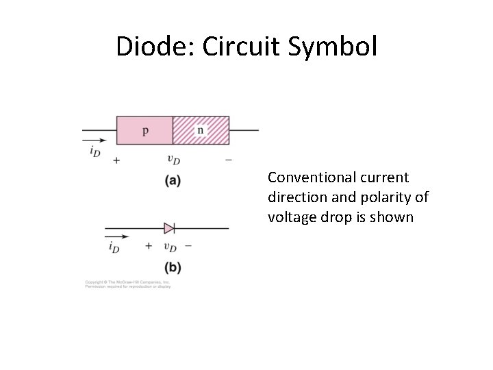
Diode: Circuit Symbol Conventional current direction and polarity of voltage drop is shown

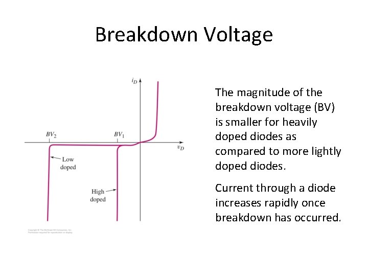
Breakdown Voltage The magnitude of the breakdown voltage (BV) is smaller for heavily doped diodes as compared to more lightly doped diodes. Current through a diode increases rapidly once breakdown has occurred.

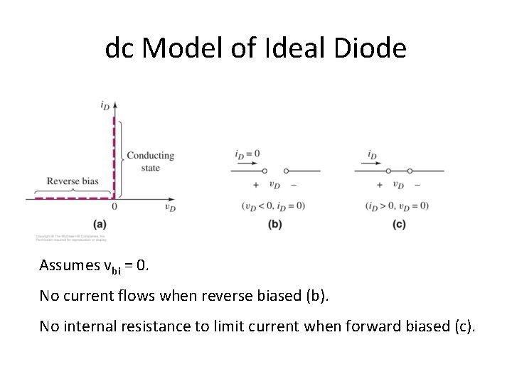
dc Model of Ideal Diode Assumes vbi = 0. No current flows when reverse biased (b). No internal resistance to limit current when forward biased (c).

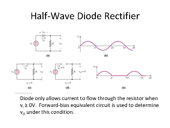
Half-Wave Diode Rectifier Diode only allows current to flow through the resistor when v. I ≥ 0 V. Forward-bias equivalent circuit is used to determine v. O under this condition.

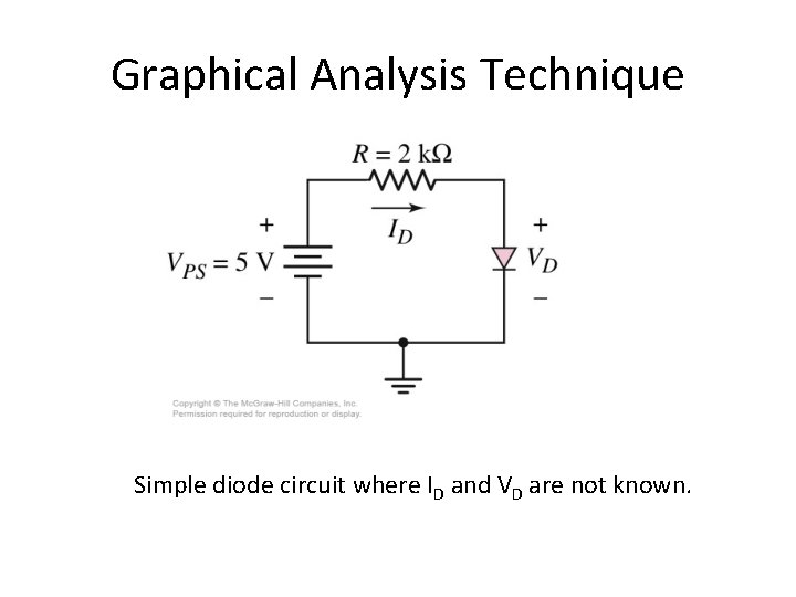
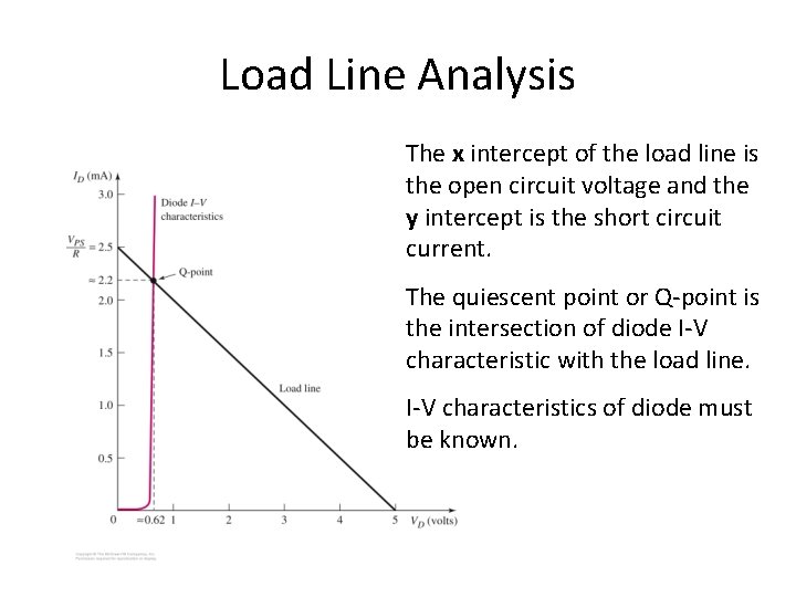
Graphical Analysis Technique Simple diode circuit where ID and VD are not known.

Load Line Analysis The x intercept of the load line is the open circuit voltage and the y intercept is the short circuit current. The quiescent point or Q-point is the intersection of diode I-V characteristic with the load line. I-V characteristics of diode must be known.
